


-
Metal halide perovskites (MHPs) are one kind of emerging semiconductor materials. The structural formula of bulk MHPs is ABX3, where A, B, and X sites are monovalent cations (e.g., Cs+, Rb+, methylamine MA+, and formamidine FA+), metal cations (e.g., Sn2+ and Pb2+), and halogen anions (e.g., Cl-, Br-, and I-), respectively. MHPs offer continuous spectral tunability from blue-violet to near-infrared regions due to their diverse chemical composition1-3. Moreover, MHPs exhibit narrow emission line widths and high colour purity owing to high defect tolerance4,5. The colour gamut of MHP emitters can reach 140% of the national television system committee (NTSC) standard3. Furthermore, the emergence of 3D bulk MHPs; low-dimensional MHP, such as layered 2D or quasi-2D perovskites6,7; colloidal perovskite quantum dots; and nanorods has revealed unique photoelectric characteristics due to their quantum and dielectric confinement effects8-12. MHP and perovskite light-emitting diodes (PeLEDs) are considered the most promising application technologies for the next-generation display and lighting field. In 2014, Tan et al. first demonstrated green and near-infrared emission PeLEDs at room temperature13. Since then, PeLEDs have undergone extensive research and continuous development resulting in rapid improvements in their performance. The external quantum efficiencies (EQEs) of green, red, and near-infrared emission devices have exceeded 20%14-21. Recently, the EQEs of blue PeLEDs have also exceeded 17%22. PeLEDs have shown performance comparable to those state-of-the-art organic and quantum dot LEDs. They exhibit unique advantages in terms of colour purity, material cost, and preparation process, which distinguishes them in the fields of wide colour-gamut displays and solid lighting.
Despite the remarkable progress, several challenges exist in achieving commercial display applications for PeLEDs. High-performance PeLEDs operate only in small active areas, as the high nonuniformity of the large-area active layers presents a major obstacle to their operation. Large-area MHP films tend to exhibit increased roughness, reduced crystalline homogeneity, and degraded optical properties, which limit the large-scale manufacturing of PeLEDs and hinder their application in large-area displays4,23,24. Most research on PeLEDs concentrates on prototype devices with a single emission pixel. However, the manufacture of high-resolution and full-colour display panels, especially emerging mini/micro-LED panels with low power consumption, high contrast, and high response speed, requires the fabrication of high-quality red-green-blue light-emitting pixel arrays. The commercialisation of PeLEDs has been significantly impeded because of their limitations in high-resolution, full-colour MHP array patterning strategies, and device integration technologies. Flexible light-emitting diode (LED) devices offer the advantages of low weight, portability, and bendability. Fabricating LEDs on flexible platforms allows these devices to exhibit greater expansibility, making them suitable for use in folding displays, wearable electronics, and biological imaging25-27. Presently, high-performance PeLEDs are mainly prepared based on rigid substrates, which limits their potential application scenarios. MHP materials exhibit solution-processable properties and intrinsic mechanical flexibility, providing prospects for the development of perovskite-based flexible optoelectronic devices.
This review summarises the representative attempts at PeLEDs in commercial display applications and discusses the key challenges and development prospects in this field. We outlined three significant technical obstacles that must be overcome to meet the needs of the consumer electronics market and level of industrial production requirements. This review discusses large-area PeLED preparations, PeLED patterning strategies, and flexible PeLED devices (Fig. 1). We introduce the mainstream fabrication strategies and limitations of large-area and patterned PeLED devices. We also discuss the research progress in flexible PeLED devices, including the modulation of the intrinsic mechanical properties of MHP materials and flexible electrode engineering. Finally, we suggest possible technical improvements for enhancing the stability of PeLEDs. We also propose research directions to accelerate the commercialisation of PeLEDs.
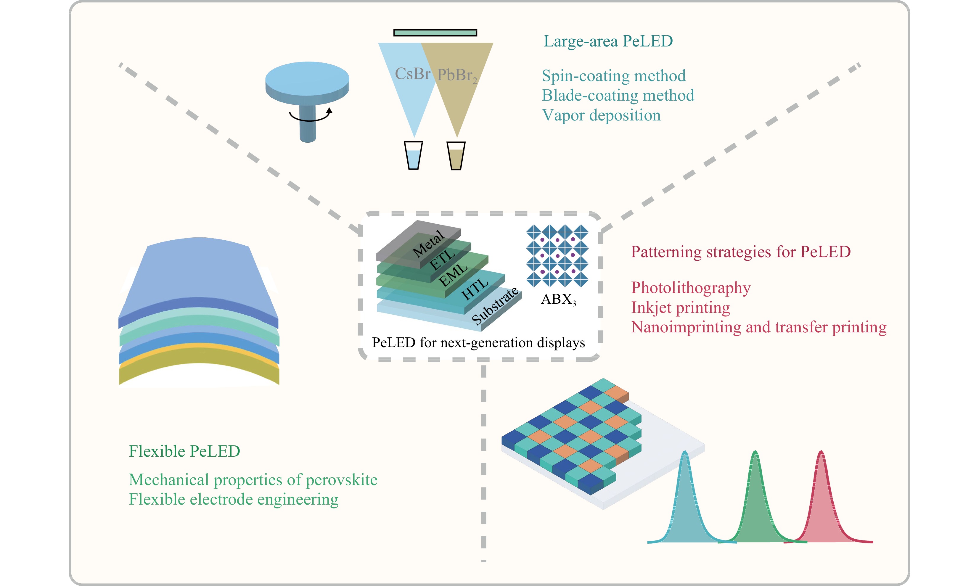
Fig. 1 Schematic diagrams of large-area PeLED preparation, patterning strategies, and flexible PeLED devices.
-
The large-scale fabrication of PeLEDs is significant for the development of display panels. However, high-performance PeLED devices produced in laboratory settings usually have an emission area less than one square centimetre28,29. When the emission region is enlarged, the MHP film shows decreased crystallinity and uniformity, resulting in low device performance24,30. These drawbacks make it challenging for PeLEDs to transfer their excellent electroluminescence (EL) features into scalable manufacturing lines. The development of a feasible large-area MHP film deposition technology is necessary to achieve large-area and high-throughput production of PeLED devices. This includes improving the existing spin-coating method and using deposition technologies that are compatible with large-scale manufacturing, such as new-type blade coating or vapour deposition methods.
-
The spin-coating method features solution processability. MHP films with flat, dense, and uniform morphologies and high crystallinity can be obtained through a simple one-step precursor coating process, which is widely used to prepare small-area LED devices31-33. Many researchers have attempted to extend high-performance devices to large-area substrates via spin coating. In 2018, Yuan et al. fabricated self-assembled core-shell structured CsPbBr3 quantum dot films using a one-step precursor coating method. The resulting films displayed a uniform and flat morphology, as well as high photoluminescence quantum yield (PLQY). This enabled the resulting green PeLEDs to deliver a recorded EQE of over 10% in a large emission area of 4.0 cm−2 from Ref. 34. Then, Zhao et al. further obtained a near-infrared PeLED device with an EQE of 12.1% in an emission area of 9.0 cm−2 from Ref. 35.
Compared with small-area devices, the performance degradation of these large-area devices can be attributed to the reduced film flatness and crystallisation uniformity. When the substrate area expands, realising homogeneous solvent diffusion/crystallization between the edge and centre regions becomes significantly challenging24. Thus, large-area MHP films prepared via the spin-coating process often show increased defect state density, decreased flatness, and generate many carrier shunting paths in the edge regions of the film.
Quasi-2D MHP films with PbX6 inorganic layers sandwiched between organic ligands show effective carrier confinement capabilities and high PLQY, making then ideal active-layer choices for developing high-efficiency LEDs. For large-area devices, it is necessary to obtain large-area quasi-2D MHP films with uniform phase component distributions. However, the conventional one-step spin-coating deposition strategy exhibits challenges in preparing uniform large-area quasi-2D MHP films36. Sun et al. found that the phase compositions across the substrate are significantly disparate, when employing the “antisolvent dropping” method for preparing large-area quasi-2D MHP films.24 The edge regions with non-uniform antisolvent diffusion demonstrate separated phase distribution, in which bulk 3D and layered 2D phases are dominant (Fig. 2a). To address this issue, they introduced a certain amount of L-norvaline into the precursor solution to partially replace the PEA+ ligand. This resulted in a low-generation-energy quasi-2D intermediate phase. This strategy allowed the quasi-2D film to exhibit a concentrated phase distribution without the use of an antisolvent. They finally extended the excellent optical performance of small-area quasi-2D films to large-area substrates and demonstrated a large-area green PeLED with a maximum EQE of 16.4% for a device active area up to 9.0 cm2 (Fig. 2b, c).
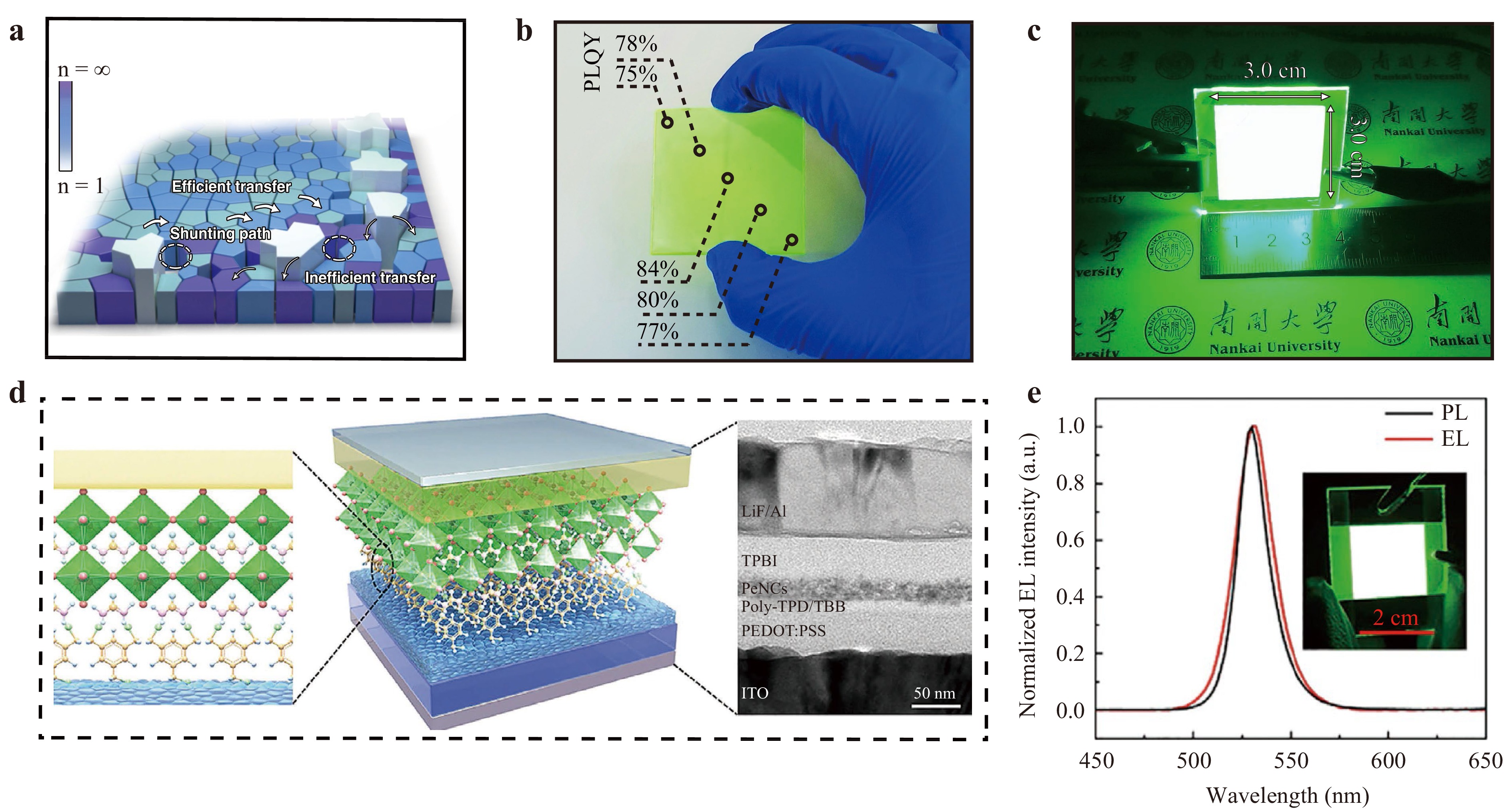
Fig. 2 Large-area PeLEDs fabricated via spin-coating method. a Schematic illustration for phase segregation and the corresponding non-radiative loss of the large-area MHP film24. b Digital photo of a large-area MHP film and the PLQY in different spots24. c Digital photo showing the uniform emission of the 3.0 × 3.0 cm2 large-area PeLED device24. d Device structure and cross-sectional transmission electron microscope (TEM) image of the TBB modified PeLED30. e Digital photo showing the uniform emission of the 2.0 × 2.0 cm2 large-area PeLED device30. Figure a is adapted with the permissions from Nature; figures b and c are reprinted with the permissions from Nature; figures d and e are reprinted with the permissions from Elsevier.
Unlike perovskite precursor solutions, perovskite nanocrystal (PNCs) inks are pre-crystallised and capped with organic ligands. Thus, the deposited PNCs films were not affected by the film crystallisation process, and inherent phase inhomogeneity in the self-assembly process was avoided. Furthermore, PNCs with efficient charge carrier confinement and fast exciton recombination generally feature a high PLQY and narrow emission line width37. PNCs thus have great potential for application in high-performance large-area PeLED preparation. Wang et al. pointed out that thermal convection during solvent evaporation reduces the uniformity and coverage of PNCs films, ultimately resulting in increased trap density30. Hence, they introduced a 1, 3, 5-tris (bromomethyl) benzene (TBB) interfacial molecular modifier. The TBB incorporated with Br can bind to the FAPbBr3 NC during the spin-coating process and deliver large-area FAPbBr3 NCs films with improved coverage, high surface flatness, and low defect state density. Using this PNCs film, they demonstrated a 4.0 cm2 green PeLED with a maximum EQE over 16% (Fig. 2d, e). This interface-modification strategy is also applicable to one-step self-assembly deposition. Recently, Kong et al. successfully demonstrated a large-area quasi-2D PeLED using betaine citrate as the interface modifier. This device, with an area of 3.5 cm × 3.5 cm, shows uniform emission and a maximum EQE exceeding 12%, making it one of the most efficient PeLEDs exceeding 10 cm−2 from Ref. 38.
-
The emission areas of PeLED devices fabricated using spin-coating methods are limited by the substrate size. Hence, the development of MHP film-coating techniques that are compatible with large-scale industrial fabrication is significant. The blade coating method, a mass-production technique, was used to prepare high-performance large-area perovskite solar cells (PSCs) (Fig. 3a)39,40. Blade-coating method is also used to prepare large-area PeLED devices41-44. Unlike the active layer in PSCs with a large grain size and high film thickness, PeLED active layers require small grain sizes to realise charge carrier confinement and a thin film for efficient carrier injection45,46. In contrast to spin-coating, MHP film deposition during the blade-coating methods involves a mass of excess solvent that cannot be removed in a short period47. To accelerate solvent evaporation, heating the substrate under high temperatures is necessary. However, achieving uniform solvent evaporation and preventing solute migration or aggregation can pose challenges in this approach23. The blade-coating method with slow and non-uniform solvent evaporation usually results in high surface roughness and heterogeneous grain size48.
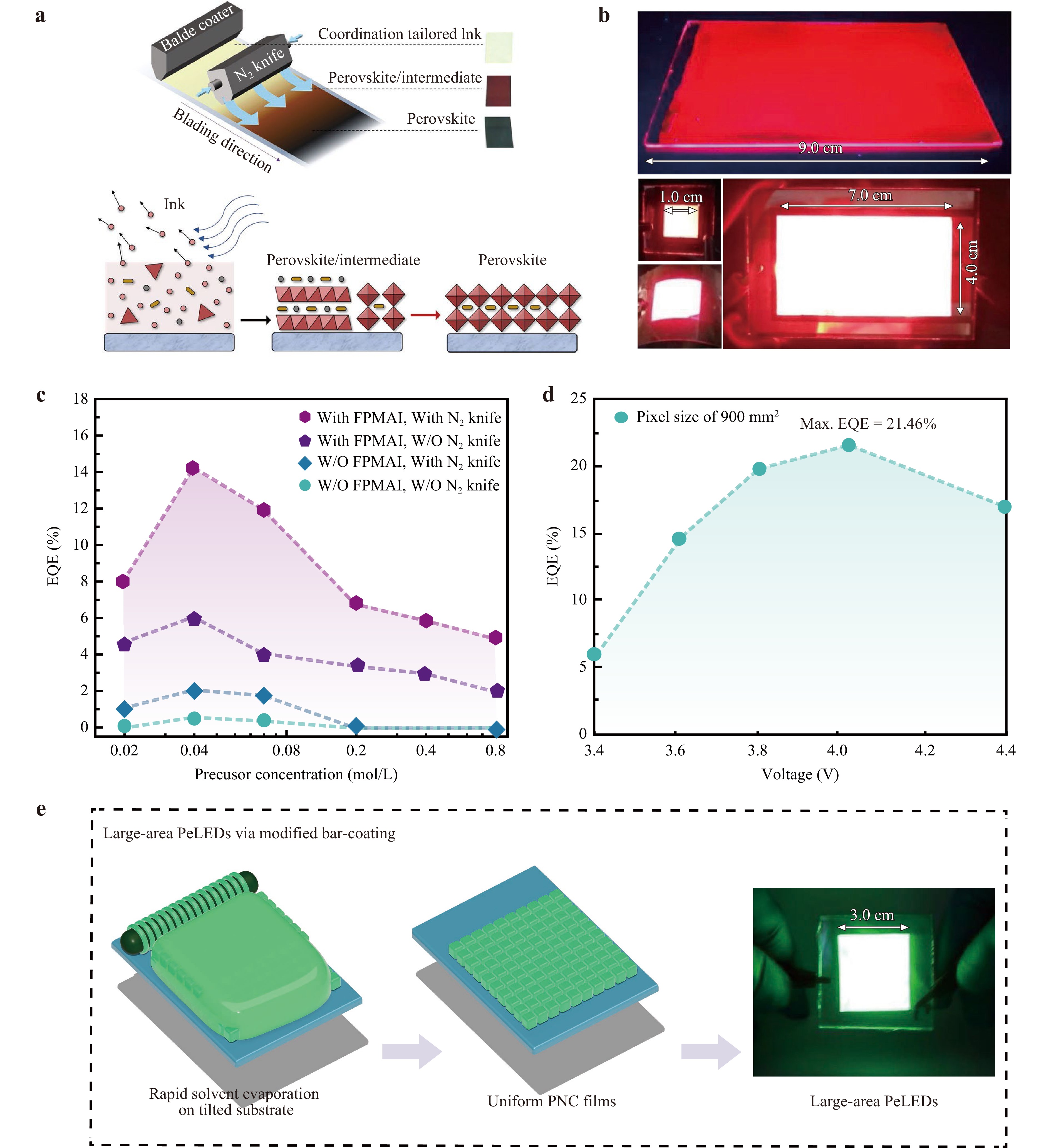
Fig. 3 Large-area PeLEDs fabricated via blade-coating method. a Schematic diagram showing N2-knife–assisted blade-coating process40. b PL and EL images of the large-area MHP films and LEDs fabricated by blade-coating method42. c Maximum EQE of the PeLEDs fabricated through different methods42. d EQE-V curves of bar-coated PeLEDs with different emission area41. e Schematic illustrations of modified bar-coating of colloidal PNCs41. Figures are adapted with the following permissions: a from AAAS; b–e from Springer Nature.
Chu et al. demonstrated a modified N2 knife-assisted low-temperature blade-coating method to overcome the inherent inhomogeneous crystallisation (Fig. 3b)42. They achieved this by increasing the number of nucleation centres, introducing excess bulky organic ammonium halides, diluting the precursor concentration, and applying additional heat to the substrate, accompanied by an N2 knife sweep to accelerate the solvent evaporation. Such procedures eliminate the gelation process and accelerate phase transformation. The resulting blade-coated near-infrared (NIR) MHP films exhibited high flatness and uniform crystallisation across the substrate. The resulting PeLEDs, with an emission area of 1.0 cm2, reach an EQE of 12.7% (Fig. 3c). The large-area blade-coating method also delivers an ultra-large area of 28 cm2, demonstrating its potential compatibility with large-scale manufacturing processes. Chen et al. demonstrated vacuum-assisted crystallisation blade coating for large-area MHP film deposition at room temperature44. In this process, the deposited precursor film was transferred to a vacuum chamber to remove excess solvent. This avoids the migration and aggregation of solutes caused by nonuniform heat transfer. Thus, they deliver a large-area PeLED with uniform green emission across an area of 3.5 × 3.5 cm2. PNC inks with high PLQY can also be used in large-area blade coating technology. The coated PNCs film avoids the optical property degradation caused by inhomogeneous crystallisation, which simplifies the blade coating process. For the blade-coating process using PNCs inks, enabling homogeneous solvent evaporation and avoiding thermal convection are crucial for achieving uniform and fully covered films. Recently, Kim developed a modified bar-coating method for preparing large-area FAPbBr3 NCs films41. This procedure involves using a wire-wound Mayer rod without air knife assistance or substrate heating (Fig. 3d, e). After bar coating, the substrate was tilted at an angle. The PNCs colloids gradually flowed downward, driven by gravity, enabling the formation of uniform PNCs films through the convective flow-capillary force-assisted assembly. Based on this technology, they fabricated large-area green PeLEDs with an EQE of 22.5 and 21.46% in emission areas of 102 and 900 mm2, respectively. These devices represent the most efficient large-area PeLED devices available (Fig. 3d).
Modulating the chemical composition and incorporating appropriate additives and surface ligands are common practices for obtaining high-quality large-area MHP films. The chemical compositions of the precursors affect the crystallisation process and ultimately lead to different film qualities. For example, all-inorganic CsPbBr3 emitting materials have low solubility and fast crystallisation rates in DMSO (dimethyl sulfoxide) and DMF (N,N-Dimethylformamide), which can easily lead to pinhole-containing MHP films. Introducing A-site components, such as MA and FA, can improve film quality and produce pinhole-free, uniform large-area films.49 Some growth modifiers have also been introduced into the precursors to improve film quality. For example, MACl is used to obtain a wider heat treatment window to improve crystallinity, which was demonstrated in both spin-coating and blade-coating processes50. The introduction of a crown into the precursor enables uniform nucleation and the growth of MHP films by exploiting the strong interaction of the crown with Cs+ and Pb2+ metal ions51. Surface ligands also influence the crystallisation process and film homogeneity of the MHP materials. Chu et al. demonstrated that the addition of excess bulk organic ammonium ligands can slow down the phase transition process of the PbI2-DMF-MAI intermediate phase, increase the nucleation density, inhibit grain overgrowth, and deliver high-quality large-area films42-43. Miao et al. demonstrated a ligand-assisted one-step scheme for forming large-area γ-CSPbI3 microcrystalline films52. 1,3-propanediamine dihydriodide was found to slow down the phase transition from the intermediate phase to the CsPbI3 phase and reduce surface defects. Thus, they demonstrated a large area deep-red light device with a peak EQE of 10.30% over an effective area of 9.0 cm2.
-
The vapour deposition technique is the most developed commercial solution for manufacturing large-scale organic LED (OLED). The vapour deposition technique has attracted considerable research interest for the fabrication of large-area MHP film fabrication53. Generally, MHP which can be obtained via thermal co-evaporation or subsequent deposition of metal/organic halide precursors (Fig. 4a). The power conversion efficiency (PCE) of perovskite solar cells fabricated by vapour deposition has reached over 24%, comparable to their solution-processed congeners54. However, performance of PeLEDs produced by vapour deposition lagged behind significantly. Several technical challenges hinder the delivery of high-quality vapour-deposited MHP emitters. The deposition process is usually accompanied by in-situ annealing to improve the quality of the films. Chen et al. confirm that high temperatures can increase the crystallinity and surface coverage of MHP film, and induce grain orientation along specific planes55. The deposited CsPbBr3 films under in situ thermal annealing at 60 °C show more homogeneous surface morphology, lower defect state density and higher PLQY compared to the films deposited at room temperature (Fig. 4b, c). They fabricated the first vapour-deposited large-area PeLED with an emission area of 14.0 cm2 (Fig. 4d). However, a high annealing temperature leads to the overgrowth of perovskite grains, resulting in a competitive relationship between the optical properties and crystallinity of the films. That is, the electrical properties and surface coverage of the film increased with increasing temperature owing to the increased crystallinity, while the PLQY of the film decreased with increasing temperature owing to the weakened carrier confinement effect. To improve the carrier recombination efficiency of films, Du et al. suggested a spatially confined vapour deposition method56. They found that 0D Cs4PbBr6 could be incorporated into a CsPbBr3 film by simply adjusting the molar ratio of CsBr to PbBr2 (Fig. 4e). Cs4PbBr6 with a broad bandgap acted as the matrix and was embedded with CsPbBr3 nanoinclusions (Fig. 4f). The Cs4PbBr6/CsPbBr3 heterojunction achieved efficient electron and hole confinement, which increased the radiative recombination rate. The spatial-confined vapour deposition method further delivered an ultra-large PeLED with an emission area of up to 40.2 cm2, and the device reached a peak EQE of 7.1%. Additionally, the device exhibited a uniform EL emission over the entire active area (Fig. 4g, h). This demonstrates the excellent compatibility of the thermal vapor deposition technique with large-area LED fabrication. In addition, it is widely known that pristine MHP films usually suffer from trap states at the surface and boundaries of the grains. For the passivation of MHP films, the solution-processed approach allows the in-situ introduction of additive molecules, such as bulk organic ligands, small-molecule Lewis bases, and conducting polymers, during the crystallisation process57,58. However, introducing these additives in the thermal evaporation process is challenging because of the large gasification temperature differences between these additive molecules and the MHP precursors. Currently, additive molecules such as PEABr and LiBr have been deposited onto MHP films by chemical vapour deposition (CVD) techniques, and the passivation effect has been demonstrated in small-area vapour-deposited devices59,60. However, the successful use of these techniques for large-area device preparation has not been reported. Overall, fabricating large-area, highly efficient PeLED devices via the vapour deposition technique requires careful control of the precursor ratios, deposition rate, growth/annealing temperature, and development of efficient defect passivation strategies.
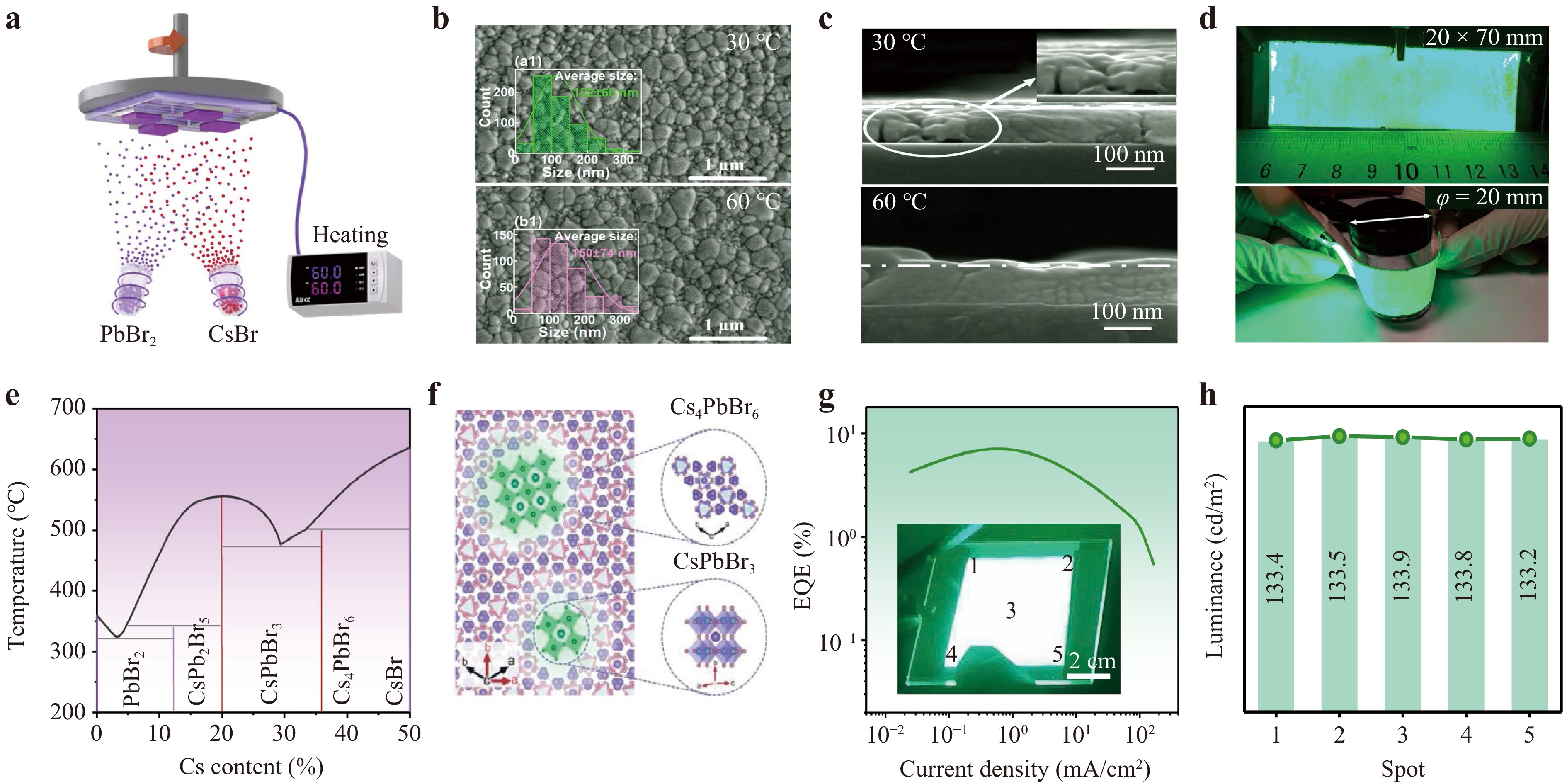
Fig. 4 Large-area PeLEDs fabricated via vapor deposition. a Schematic diagram of the thermal vacuum co-evaporation deposition process55. Scanning electron microscope (SEM) images of CsPbBr3 films deposited at different temperatures: b Top-view and c cross-sectional view55. d Photograph of a large-area PeLED fabricated via vapor deposition55. e Phase diagram of CsBr-PbBr2 binary system56. f Schematic representation of CsPbBr3 nano-inclusions embedded in the Cs4PbBr6 matrix56. g EQE-current density curve of the large-area PeLED, inset is the digital photo of the LED in operation56. h The luminance of five marked spots corresponding to the inset picture in panel g56. Figures are adapted with the following permissions: a–d from ACS; e–h from Springer Nature.
-
Micro- or nano-arrays and their fabrication methods are essential for developing advanced integrated optoelectronic platforms. Precise and highly integrated pixels are prerequisites for incorporating these emerging MHP into full-colour high-resolution displays. Periodic micro- or nano-patterned optical films can also enable the unprecedented optoelectronic performance of MHP. For example, periodic photonic crystals can effectively improve the outcoupling efficiency of LED devices61, the use of one-dimensional periodic nano grating structures provide polarized light detection capabilities62, and the MHP patterns with periodic refractive index structures enable the construction of effective distributed Bragg resonators63. Tremendous efforts have been devoted to developing structured MHP. These materials have potential applications in various optical devices, such as, laser, super-surface, and nonlinear optic devices64,65. Several previous reviews have summarized strategies for the preparation of patterned optical MHP films66,67. However, integrating patterned MHP films into full-colour high-resolution electroluminescent devices remains a challenge. Delivering high-performance patterned PeLEDs requires pattern strategies compatible with the existing workflows in LED device building. Additionally, these strategies should achieve high optical performance and low electrical loss. In this section, we focus on the application of patterned MHP arrays to LED devices. We introduce pattern strategies for high-resolution MHP active layers. These include mask-assisted photolithography technologies, mask-free jet printing methods, nanoimprinting, and transfer printing strategies.
-
Photolithography is a powerful method for fabricating high-resolution MHP patterns. Photolithography technologies are typically divided into top-down and bottom-up approaches. The top-down method utilises an etching gas/developer to etch the deposited MHP films and obtain the target nanostructures directly. The standard top-down scheme consists involves the following steps: a) spin coating of the photoresist onto the MHP film, b) exposure to UV or X-rays, c) development, and d) plasma gas etching. In this procedure, both the photoresist and the MHP film were etched. However, owing to the inherent chemical instability of MHP materials, it is challenging to maintain their initial optical properties after the commonly used polar developer treatment. Harwell et al. introduced an easily removable poly(methyl methacrylate) (PMMA) spacer layer between the commercially available SU-8 photoresist layer and MHP film, to protect the MHP films from polar solvents (Fig. 5a)68. The patterned microdisks show a minor diameter of 3 μm with low surface roughness, maintaining about 75% PLQY of the starting point. Their work also demonstrated a two-colour pattern (Fig. 5b). These MHP arrays have become an effective alternative for reducing the extremely high cost of epitaxially integrated RGB micro-LEDs via colour conversion and are expected to solve the low EQE faced by red micro-LED chips69.
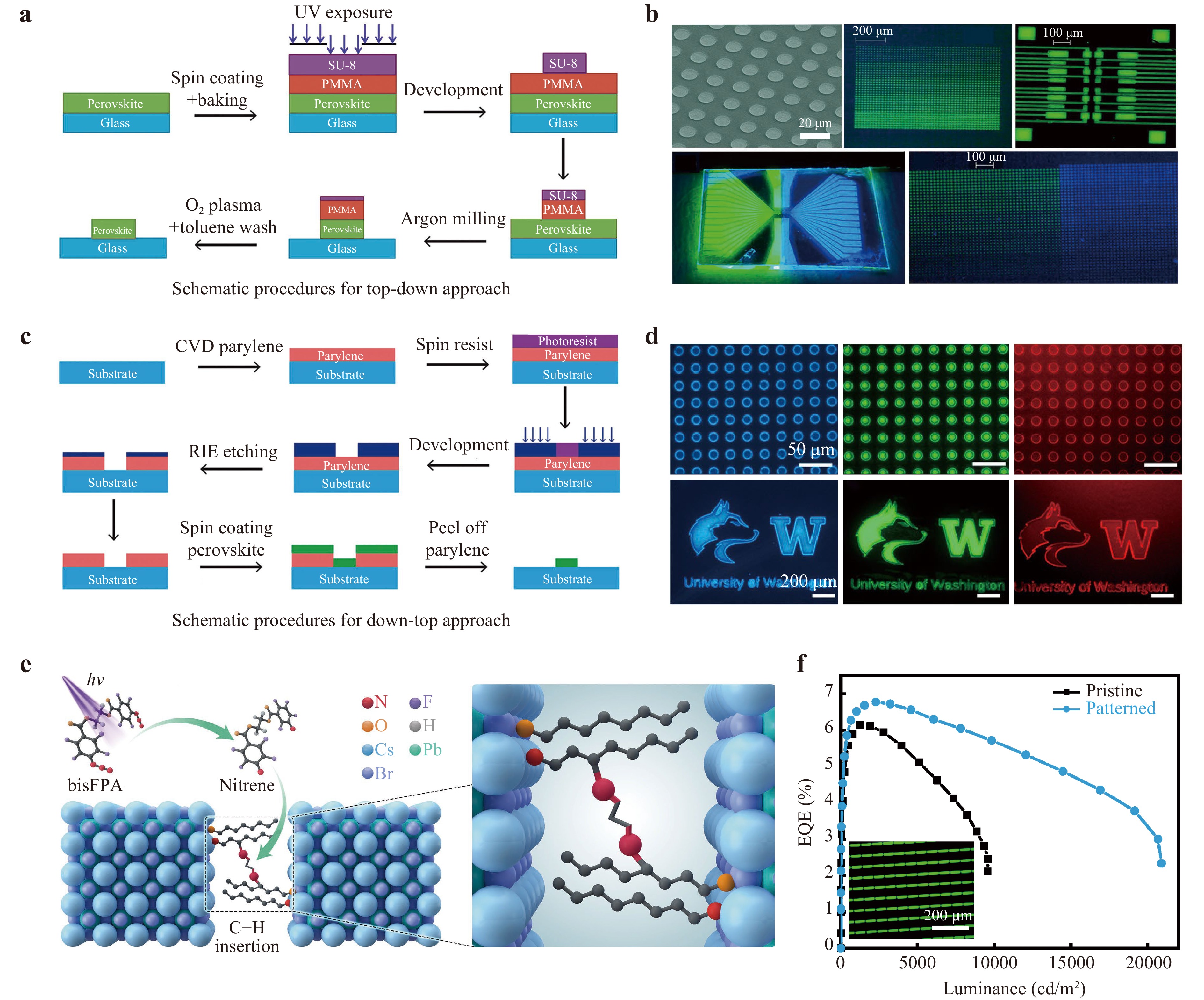
Fig. 5 Photolithography for MHPs. a Schematic diagram of the top-down lithography patterning process68. b SEM and PL images of the patterned MHP films, fabricated via top-down lithography68. c Schematic diagram of the down-top lithography patterning process71. d PL images of the patterned MHP films fabricated via down-top lithography71. e Schematic diagram of the photo-crosslinking chemistry of ligands on PNCs73. f EQE-luminance curves of pristine and patterned devices. Insets show an EL image of the patterned PeLED73. Figures are adapted with the following permissions: a–d from ACS; e and f from AAAS.
This conventional top-down scheme demonstrated high-throughput and universal properties for MHP film patterns. However, the highly reactive plasma etching gas caused significant damage to the edge region of the nanostructure. For example, the commonly used oxygen or SF6 plasma etching gases tend to chemically attack and degrade the organic components of the MHP film and induce phase transitions in these regions, resulting in surface defect states and high roughness70. Given this, exploring a pattern program that does not require etching steps is significant. The bottom-up approach uses photolithography to generate groove templates. Perovskite was then deposited on the template. After lift-off of the underlying template, patterned arrays were easily obtained (Fig. 5c). In this procedure, the MHP films are not directly exposed to UV light, X-ray light, or etching gas, and no polar solvent is required, thus preventing the degradation of MHPs. Zou et al., using a patterned parylene film as a mechanical-peelable substrate and demonstrated the first green pixelated MHP micro-LED arrays via bottom-up approach (Fig. 5d)71. The patterned devices showed a maximum EQE of 1.24% and luminance up to 13,043 cd/m2.
The direct optical patterning of perovskite nanocrystals with ligand cross-linker (DOPPLCER) technology represents another alternative that does not require etching. The surface ligand with light driven decomposable, polymeric, or cross linkable characteristics is the key to realize film patterning72. The covalent bonding reaction of photoactive ligand at the grain surface introduces MHP stability contrast in the solvent, thus forming microscale patterns after the development step. Liu et al. uses bisazides (nitrene precursors) as photoactive additives to initiate cross link of adjacent alkyl ligands73. Under UV irradiation, the bisazides create highly reactive singlet nitrene radicals and covalently bind the adjacent long alkyl chains via covalent C-N bonds. Furthermore, by carrying out the development procedure with nonpolar solvents, the unexposed NCs were removed, and a cross-linked MHP NCs network with the desired pattern was formed (Fig. 5e). Moreover, repeating this DOPPLCER process allowed for the sequential deposition of different MHP NCs, thus enabling the formation of multicoloured patterns. To demonstrate the excellent compatibility of the DOPPLCER process with established PeLED fabrication workflows, patterned arrays were further integrated into LED devices. The obtained emission pixels had a length and width of 50 and 10 µm, respectively . The patterned devices achieved a maximum EQE of 6.8%, demonstrating the feasibility of DOPPLCER for realising micro-LED displays (Fig. 5f). In addition, other etching-free schemes, such as direct laser writing which induce in situ crystallisation of precursors by providing high energy in a restricted region, also provide opportunities for MHP patterning74. However, the compatibility of these techniques with electroluminescent device manufacturing processes remains to be determined.
-
Inkjet printing is a mask-free patterning method that adds a functional ink to the substrate surface. It is an environmentally friendly, high-material-utilisation technology with the potential to meet the needs of large-scale commercial production. Inkjet printing technology does not depend on the nature of the substrate itself. Hence, it can be used to print on both rigid and flexible/stretchable materials. The inkjet-printing process also demonstrated high compatibility with large-area flexible devices. Since 2014, inkjet printing technology has been used to prepare MHP arrays for application in solar cells and photoelectric detectors75,76.
The inkjet printing process of MHP generally consists of three steps: a) ejecting a volume of MHP ink using a voltage- or air-pressure-controlled nozzle, b) filling the ink to a specified location, and c) drying or crystallising the dispersed ink in situ to form a patterned array (Fig. 6a). Optimal design of the MHP ink is vital for high-resolution inkjet printing. The MHP inks used can be classified as presynthesized colloidal NCs solutions or noncrystalline precursor solutions. High-quality colloidal NCs with air-stable, transparent, and well-dispersed properties can avoid uneven nucleation and crystallisation. As a result, they were first employed in the inkjet printing of MHP arrays77. In 2020, the first inkjet-printed PeLED, printed using FA0.3Cs0.7PbBr3 quantum dots ink, obtained an EQE of 2.8% with a pixel density of 120 pixels per inch (PPI), demonstrating the potential of inkjet printing technology in preparing high-resolution PeLEDs78. During the printing process, the printed nanostructure arrays often face “coffee ring” effects due to a capillary flow rising from the different evaporation rates between the edge and inside of the ink droplet79. Egregious “coffee ring” effect accompanied with crystalline defects further leads to severe non-radiative recombination, which reduces the device’s resolution and luminescence uniformity. Wei et al. proposed the ternary-solvent-ink strategy to prolong the Marangoni flow and suppress the “coffee ring” effect80. The Marangoni flow describes the flow of a solvent from a low surface tension region to a high surface tension region. In their ternary-solvent-ink strategy, the introduced n-nonane balances the boiling point and surface tension. Additionally, their strategy builds up gradient volatilisation and enhances the evaporation flow (Fig. 6b). As a result, the aggregation of MHP quantum dots is inhibited significantly, and the “coffee ring” effect is relieved. They printed MHP quantum dots arrays with a resolution of 250 PPI (Fig. 6c). They also obtained a PeLED with a peak EQE of 8.54%. Recently, wang et al. modified the contact properties between the MHP ink and HTL(hole transport layer) by introducing a poly[(9,9-bis(3′-((N,N-dimethyl)-Nethylammonium)-propyl)-2,7-fluorene)-alt-2,7-(9,9-dioctylfluorene)] dibromide (PFN-Br) polar polymer81. They derived printed green quasi-2D PeLEDs with a peak EQE exceeding 10%, setting a new record for the performance of inkjet-printed monochromatic PeLEDs to date. Multicolour patterns using inkjet printing technology do not require a protective layer to prevent the erosion of the predeposited arrays. This feature provides distinct advantages in full-colour matrix manufacturing. The Full-colour MHP matrix devices with a colour gamut greater than 100% (NTSC 1931) have been implemented82. In general, inkjet printing technology represents the most promising development for the mass production of PeLEDs. However, the preparation of PeLEDs based on inkjet printing technology remains is still in its early stages. Systematic guidance schemes for optimizing printing parameters and ink composition must be established to produce inkjet-printed PeLEDs with a high resolution and efficiency.
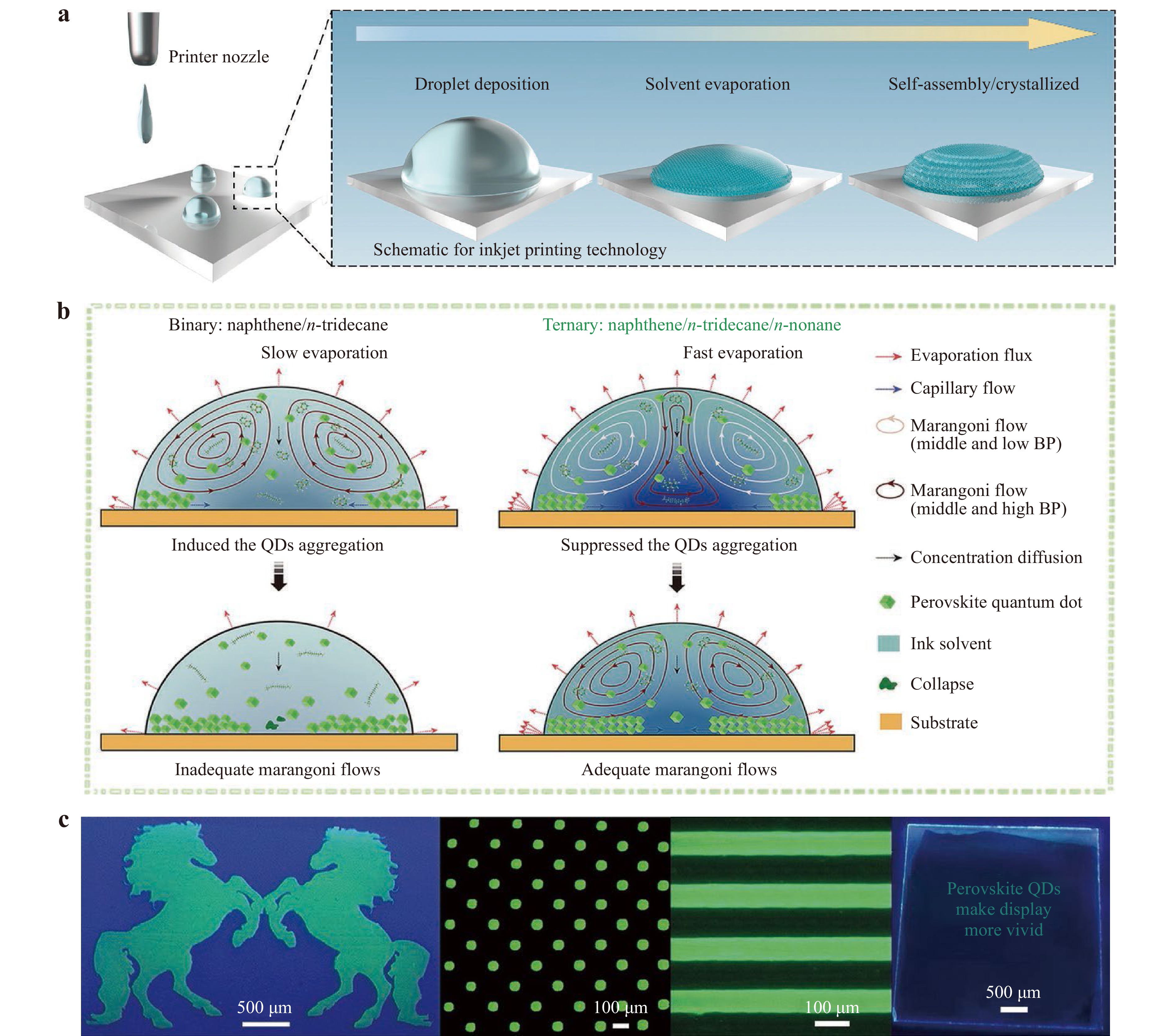
Fig. 6 Inkjet printing for MHPs. a Schematic diagram of the inkjet-printing process77. b Schematic diagram of the evaporation, Marangoni flow, and capillary flow processes in binary and ternary-solvent-ink systems80. c The fluorescence optical microscopy image of different inkjet-printed MHP films80. Figure a is adapted with the permissions from ACS; figures b and c are reproduced with the permissions from Wiley-VCH.
-
Nanoimprinting is widely used as a high-throughput and low-cost method for nanoscale printing. Nanoimprinting, also known as soft lithography, is more flexible than conventional lithography. Nanoimprinting allows for the creation of patterns without accuracy limitations caused by light scattering and can be applied to complex three-dimensional structures or flexible materials. Mainstream MHP nanoimprinting technology is based on a template-confined perovskite growth strategy. This technique requires a preproduced imprint mould with an inverse pattern. Nanoscale MHP patterns were prepared by imprinting the precursors with a stamp, followed by annealing. To restrict crystallisation in the predesigned layouts, the film must be in a wet state before imprinting. The solvent composition of the precursor and annealing temperature should be precisely controlled to obtain a gel film with plasticity. Specifically, under an appropriate pressure and thermal annealing, patterned crystals can be formed via directional deformation and solvent evaporation (Fig. 7a). The imprinting mould is the key to creating patterned structures during the nanoimprinting process. An ideal mould should be chemically inert, isotropic, deformable, and have a low surface binding energy for easy release. Polymer films such as polydimethylsiloxane (PDMS), heat-curing photoresists, and silicon are commonly used mould materials83-85. MHP micro-nano structures prepared using the nanoimprinting technique were first reported by Wang et al86. They obtained nanopore arrays with a diameter of 275 nm and a nanogrid with a width of 270 nm by using patterned silicon as the imprint mould (Fig. 7b). These nanostructures have dimensions close to the optical diffraction limit, demonstrating the potential of nanoimprinting technology for achieving ultrafine patterning. So far, nanoimprinted MHP microstructures have been used to create MHP-based optical devices such as super surfaces and distributed feedback lasers87,88. The MHP patterns prepared using the nanoimprinting technique also exhibit improved crystallinity, surface morphology, and priority orientation in crystals89. A pressure is applied parallel to the normal vector of the wet MHP film during restricted growth. This pressure inhibits out-of-plane grain growth. Thus, MHP grains form tightly packed columnar structures by reorienting toward the direction with low surface energy. Such surface-energy-driven growth enhanced the crystallisation quality, resulting in a dense and smooth film surface (Fig. 7c). Although nanoimprinting provides a simple, high-precision patterning scheme, its application in high-resolution full-colour MHP electroluminescent devices remains challenging. The nucleation and crystallisation behaviours of restricted growth are difficult to control. The crystallisation of the precursor/gel film in the confined space was affected by the uniformity of the applied mechanical stress. In addition, owing to their wet chemical properties, nanoimprinting schemes are not compatible with multicolour patterning.
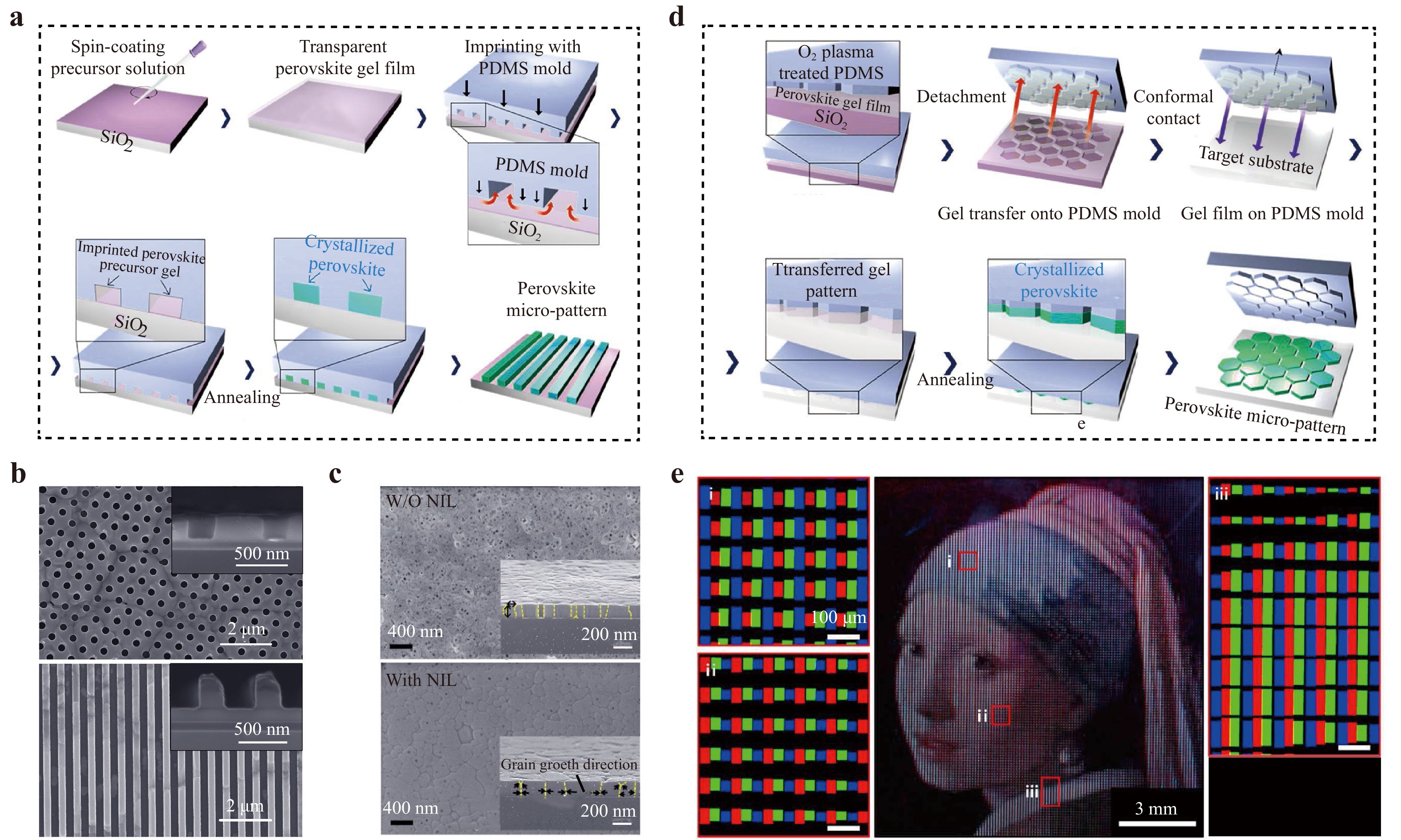
Fig. 7 Nanoimprinting and transfer printing for MHPs. a Schematic diagram of the gel nanoimprinting of MHP patterns90. b SEM of nonimprinted MHP thin film imprinted with a Si nanopillar mold86. c SEM images of MAPbBr3 thin films with and without nanoimprint lithography89. d Schematic diagram of the gel transfer printing of MHP patterns90. e PL images of multicolour transfer pattered MHP pixels showing the Girl with a Pearl Earring painting by J. Vermeer. Insets (i) to (iii) are PL images in selected areas92. Figures are adapted with the following permissions: a–d from ACS and e from AAAS.
Transfer printing can be combined with nanoimprinting to overcome the disadvantages of multicolour patterning. Jeong et al. combined conventional nanoimprinting and transfer printing90. By utilizing gel-assisted transfer printing, they were able to expand the range of target substrates and further broaden the application of this technique in different optoelectronic systems. Precise control of the adhesion between the imprinting mould and MHP film is the key to achieve high-quality imprint-transfer printing. When only the nanoimprinting step was performed, the topographically patterned PDMS interacted directly with the gel-state precursor film. The PDMS mould can be easily peeled off after annealing, owing to the extremely low surface binding energy of PDMS (19.8 mJ m–2) compared to the most used inorganic oxide substrates (>200 mJ m–2)91. However, for the transfer of MHP films, O2 plasma was used to improve the adhesion of PDMS, that is, solvent-assisted gel nanoimprinting requires weak adhesion, whereas transfer printing needs strong adhesion of the MHP film to the PDMS mould (Fig. 7d). Because the transfer process does not use wet chemicals, no solvent orthogonality is involved. Hence, the cross-contamination of different colour pixels is avoided. Transfer-printing technology using polydimethylsiloxane (PDMS) and other elastic stamps has become a reliable option for high-resolution full-colour MHP pattern manufacturing. Recently, MHP microstructures with transfer yields up to 100% and resolutions of 2,550 PPI have been achieved92. Micro-PeLED based on these patterned arrays has exhibited comparable electroluminescent properties to rotational-coated congeners. Thus, a remarkable EQE of 15.3% for red devices and 14.8% for green devices have been realized, which are much higher than those of printed or photolithographed PeLEDs reported to date. In addition, the multiple sequential transfer printing strategy allowed the multicolour microarrays fabrication (Fig. 7e). Multiple-transfer white PeLEDs based on red and sky-blue MHP microstrips have also been reported93.
Overall, compared to these mainstream patterning strategies, photolithography is a straightforward and effective patterning technique that demonstrates versatility. It is compatible with various MHP materials and current commercial lithography processes. However, photolithography is expensive for large-area patterning. In addition, the erosion of MHP materials by etching gases, developers, and photoresists cannot be ignored. However, the performance of patterned PeLEDs based on lithography has lagged. The inkjet-printing process is not limited by the substrate material and demonstrates a workflow compatible with existing PeLED manufacturing. Inkjet printing technology is easy for multicolor patterning. Thus, inkjet printing is a feasible technology for developing new-generation full-colour display devices. However, inkjet-printing technology still faces the challenge of restricted resolution. Besides, the “coffee ring” effect reduces the device performance and pattern uniformity. Nanoimprinting technology overcomes the accuracy limitation caused by light scattering and has unparalleled advantages. Transfer printing technology, which was developed from nanoimprinting, provides a multicolor high-precision patterning solution. Nanoimprinting and transfer printing technologies are non-destructive patterning schemes. The performance of PeLEDs fabricated via nanoimprinting or transfer printing was comparable to that of PeLEDs prepared via spin-coating. However, nanoimprinting and transfer printing of MHP films are still in the early stages of development. The development of large-scale, full-colour PeLED devices requires further research on stamp preparation, heat treatment, interface modulation, and other imprinting processes.
-
Flexible LEDs have become revolutionary devices for various potential applications, such as portable wearable displays and biomedical imaging (Fig. 8a)94. In this section, we briefly introduce the progress of flexible perovskite light-emitting diodes (FPeLEDs). Here, we describe the strategies for regulation of the mechanical properties of MHP-emitting layers in flexible and stretchable devices. The relationship between the structural optimisation and material optoelectronic properties is also explained. We review the electrode materials compatible with FPeLEDs, such as structured metals, conductive polymers, low-dimensional carbon materials, and their composites. Comprehensive improvement strategies for candidate material parameters such as flexibility, conductivity, and transmittance have also been proposed. We also discuss interfacial and energy-level engineering to improve the compatibility of these electrodes with the MHP active layer.
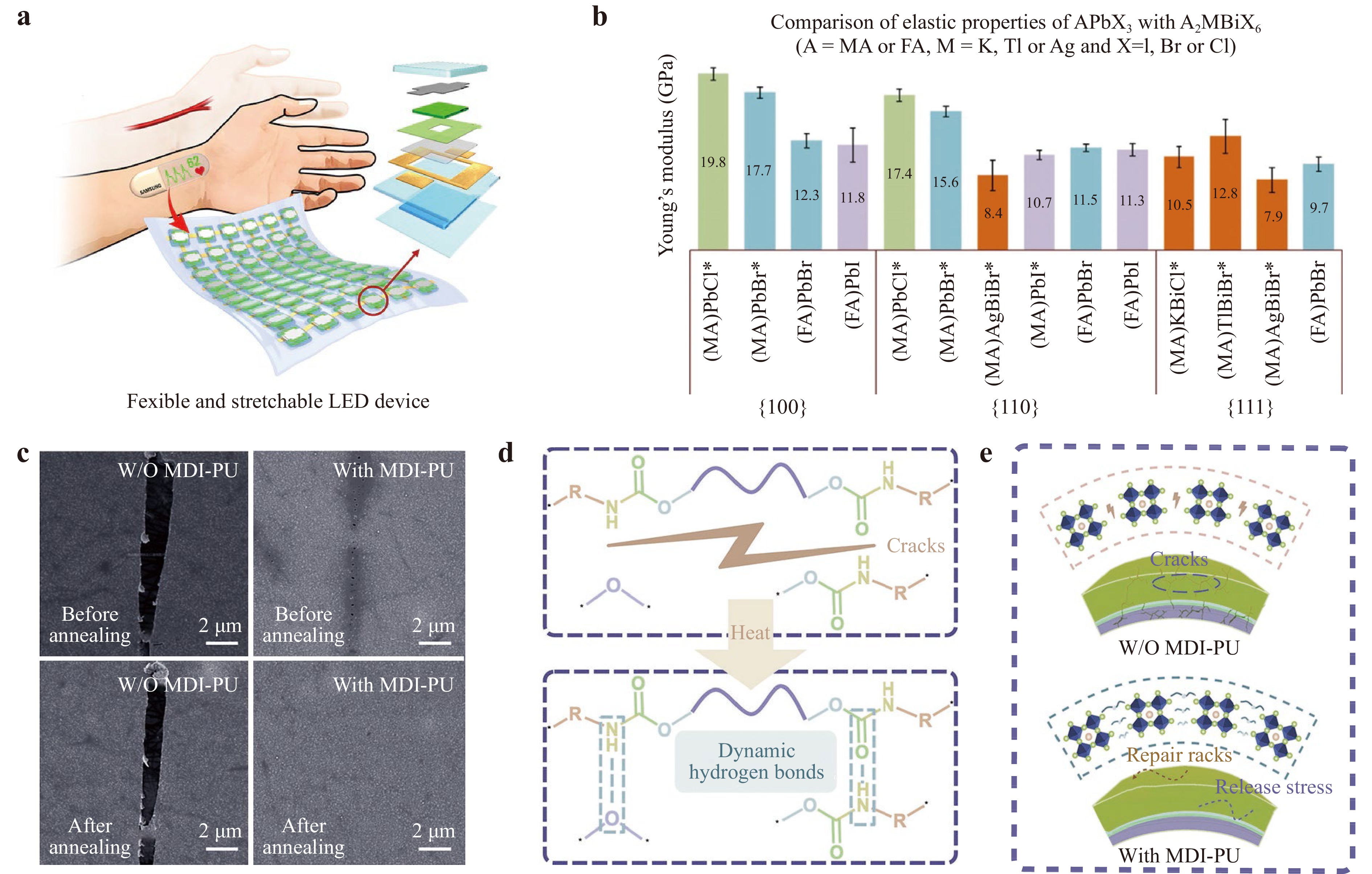
Fig. 8 Mechanical properties modulation for MHPs. a Schematic diagram of a typical application of the flexible and stretchable LED device94. b Young’s moduli of single and double MHPs normal to the different planes96. c SEM images of the cracks in MHP films with and without MDI-PU additive102. d Schematic diagram of the intra/intermolecular hydrogen bonds in the MDI-PU containing MHP films102. e Schematic diagram of the self-healing process in the MDI-PU-containing MHP films102. Figure a is adapted with the permissions from AAAS; figure b is reproduced with the permissions from Wiley-VCH; figures c–e are adapted with the permissions from ACS.
-
MHP materials with low shear moduli and mechanical stiffnesses are considered potential materials for flexible, stretchable, and wearable display devices. MHPs with high chemical and structural freedom allow the modulation of their mechanical properties via composition tuning. The mechanical properties of bulk MHPs are primarily determined by their inorganic frameworks, which consist of halides and metal ions (Fig. 8b), because of difference in electronegativity between the halogen ions. The halogen ions Cl-, Br-, and I- exhibit a gradual decrease in electronegativity, which results in a gradual weakening of the Pb-X bonding strength and an increase in the ductility of MHP inorganic frameworks95,96. Similarly, the metal cations can also affect the Pb-X bonding strengths and influence the mechanical properties of MHP. The Young’s moduli of tin-based perovskites are generally higher than those of their Pb-based counterparts because of the robust B-X combination97. Trivalent and monovalent cation-substituted double perovskites feature increased inorganic framework deformation response to external stresses because of the weak Pb-X bonds98. The dimensionality and aggregate state structure of MHP materials correlate with their mechanical properties. Two-dimensional layered perovskite and zero-dimensional perovskite nanocrystal films have higher ductilities than bulk materials because of the flexible organic ligands on their surfaces. The layered two-dimensional MHP with the (R-NH3)2An-1BnX3n+1 molecular structure consisted of inorganic PbX6 layers sandwiched between two organic cation layers. Weak intermolecular interactions between the organic and PbX6 layers allows a certain degree of interlayer slip under external stress. Two-dimensional perovskite films exhibited a higher cohesion energy than the bulk material, implying a higher resistance to crack propagation. Zhao et al. found that the improvement in mechanical properties was more pronounced for larger volume cation-containing films99. MHP with long alkyl chain cations provides a greater stretching distance for the structure collapse. In other words, the low stiffness of the alkyl chains leads to plastic energy dissipation.
Several additives have also been introduced to improve the mechanical ductility of the MHP active layers. Polymers with high elongation at break, such as poly(ethylene oxide) (PEO) and styrene-based segmented copolymers (e.g., SEBS), are widely introduced into the active layer to suppress segregation between neighbouring crystals under tensile stress100,101. These polymer additives were effectively filled in the grain boundaries to ensure a continuous pinhole-free film and suppress non-radiative leakage current. Qian et al. proposed a bionic structural design for a self-healing flexible MHP composite film based on a diphenylmethane diisocyanate polyurethane (MDI-PU) elastomer102. The harmful cracks caused by deformation in the active layer can be effectively self-healed after heat treatment, by the action of MDI-PU intra-/intermolecular hydrogen bonds (Fig. 8c–e). Thus, the bending resistance of the MHP film was significantly improved. The demonstrated blue flexible PeLED achieved a record EQE of 13.5% and maintained more than 80% of its initial efficiency after 2,000 cycles of repeated bending. Cross-linkable additives that can build interlocking networks between adjacent grains have also been used to improve MHPs’ flexibility significantly. Sun et al. added ethylcellulose (EC) to CsPbI3 NCs and constructed a ligand-halide perovskite crosslinked network via hydrogen bonding103. The crosslinked FPeLED exhibited an EQE of 12.1%, a high resistance to deformation, and a stable luminescence after bending 1,000 times.
-
Flexible electrodes are key components that affect the mechanical flexibility and electrical properties of FPeLEDs. The electrodes used in FPeLEDs must satisfy the requirements of high resilience, robustness, transmittance, and conductivity. In addition, these electrodes require energy-level matching with the transfer/emission layers and must be compatible with the fabrication workflows of the present PeLEDs. Inorganic oxides, structured metals, conducting polymers, and their composites have been used to fabricate FPeLEDs (Fig. 9a). Herein, we briefly describe the development of these flexible electrode materials and summarise the multidimensional strategies for improving their optical and electrical properties.
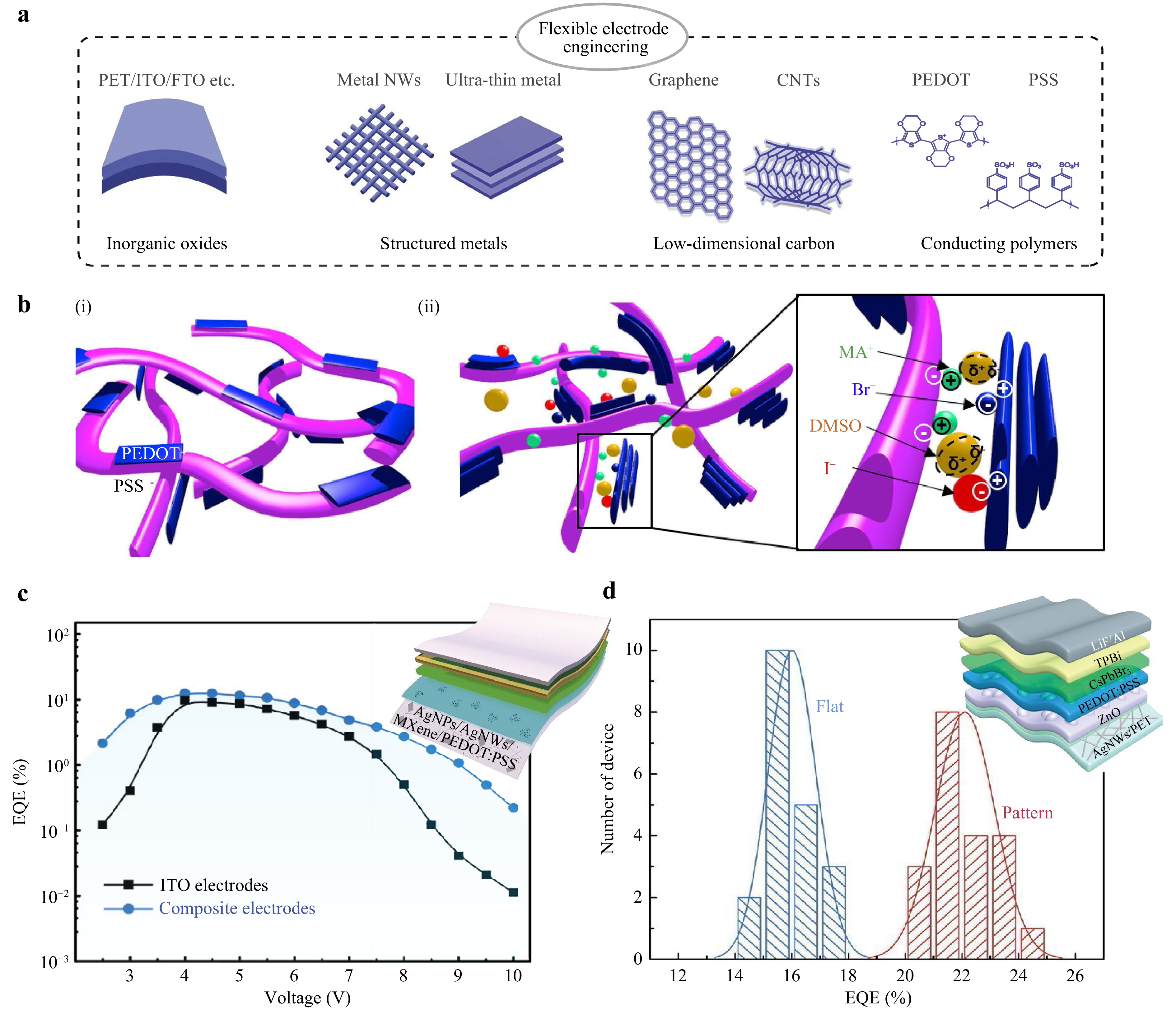
Fig. 9 Flexible electrode engineering for FPeLEDs. a Schematic illustration of some flexible electrode candidates. b Schematic diagram of the domain separation of PEDOT+ and PSS- chains with alkylammonium halide and DMSO additives109. c EQE−V curves of PeLEDs based on ITO and flexible composite electrodes; inset is the device structure of the flexible PeLED112. d Histograms of the peak EQEs of flexible PeLEDs with flat electrode and light outcoupling structure; inset is the device structure of the flexible PeLED106. Figure b is reproduced with the permissions from Wiley-VCH; figures c and d are adapted with the permissions from ACS.
The metal electrodes used on the light output side, such as ultrathin metal films or metal nanowires (NWs), should be structured to ensure sufficient transmittance. Lu et al. used Ag and ultrathin Au as the cathode and anode of FPeLEDs, respectively104. An ultrasmooth Ag film peeled onto a silicon substrate using a flexible polymer was used as the bottom electrode to avoid undesirable leakage current. The bottom electrode had a MoO3/Au/MoO3 multilayered structure that combined high electrical conductivity and transmittance. These all-metal electrodes have advantages in terms of flexibility and mechanical robustness and show excellent energy band alignment for efficient charge transport and recombination. The obtained FPeLED delivered an EQE of 8.2% and maintained its performance after 1,000 repetitions of bending. Metal NWs have also become one of the most popular electrode materials for flexible optoelectronic devices owing to their high transmittance, mechanical flexibility, and solution processability. The main weaknesses of metal NWs electrodes are their high surface roughness and consequent current-leakage channels. To obtain a dense and flat metal NWs network electrode, an inverted film-processing method was performed by embedding the metal NWs in a polymer matrix and then stripping the coated electrodes from rigid substrates105. The electrical properties of high-quality AgNW electrodes are comparable to those of sputtered ITO (indium-tin oxide)-on-glass substrates. Thus, AgNW-based electrodes are the most used electrodes in high-performance flexible devices. FPeLED devices based on AgNW electrodes have achieved EQEs of more than 10 and 20% for blue and green emissions102,106.
Conducting polymers, such as PEDOT:PSS, have significantly better mechanical flexibility and stretchability than inorganic electrode materials. In PEDOT:PSS, PEDOT (poly(3,4-ethylenedioxythiophene)) is a conductive polymer with a π - π conjugated backbone. Insulating polystyrene sulfonate (PSS) was used to remove the electrons from PEDOT and increase the hole density. The pristine PEDOT:PSS films have a low electrical conductivity of about 0.08–0.76 S/cm107. To improve the electrical conductivity of the electrode, it is necessary to remove insulating PSS chains which are excessive. A universal method is to separate insulating molecules (PSS) of PEDOT:PSS, and induce the formation of ordered π-π stacked conducting chain (PEDOT) domains. This can be achieved by incorporating polar solvents, ionic liquids, or acids108. However, removing insulating PSS chains usually reduces the work function (WF) of PEDOT:PSS, making the energy level of PeLED more mismatched. The addition of fluorinated additives with high functionalities, such as a perfluorinated ionomer (PFI), tetrafluoroethylene-perfluoro-3,6-dioxa-4-methyl-7-octenesulfonic acid copolymer, and Zonyl FS-300, can increase the anode WF and reduce exciton quenching at the PEDOT:PSS/MHP interface. Jeong et al. reported a scheme to obtain ideal conducting polymer anodes with a high work function and conductivity by co-doping PEDOT:PSS with alkylammonium halides and PFI109. The addition of alkylammonium halides formed a PEDOT-rich nanofibre network, whereas PFI ensured the high WF of the anode (Fig. 9b). Thus, the conducting polymer was used as both anode and hole injection layers, achieving a polycrystalline PeLED with an EQE of 10.93%.
In addition to the above commonly used flexible electrode materials, low-dimensional carbon materials such as graphene and carbon nanotubes (CNTs) have also been used to build FPeLED devices110. However, these low-dimensional carbon materials suffer from low electrical conductivity, low WF, and severe surface exciton quenching95,111. Thus far, the EL performance of FPeLEDs based on low-dimensional carbon materials poorer than that of their counterparts. In addition to flexible electrodes based on a single material, composites with multiple flexible-conductive materials are preferred for high-performance FPeLEDs. Cao et al. demonstrated FPeLEDs utilizing a blend of 0D Ag nanoparticles (AgNPs), 1D AgNWs, 2D MXene, and 3D PEDOT:PSS (0D-1D-2D-3D) architecture (Fig. 9c)112. This composite electrode combines the excellent thermal conductivity of MXene, electrical properties of inorganic metal materials, and flat surface of PEDOT:PSS. The obtained FPeLEDs obtained an EQE of 16.5%. Additionally, they fabricated a large-area device (8.0 cm2) with significantly enhanced mechanical stability. Shen et al. reported a composite electrode based on a AgNW/ZnO/PEDOT:PSS structure (Fig. 9d)106. Randomly distributed AgNWs were spin-coated onto PET as the anode. Furthermore, a ZnO thin film was used to fill the voids between the AgNWs. The PEDOT:PSS layer was then spin-coated onto AgNW/ZnO to facilitate hole injection. The prepared composite electrode possesses high surface flatness and thermal stability, and avoids the exciton quenching of the emitter on the AgNW surface. The obtained planar FPeLEDs achieved an EQE of 17.1%. A record EQE of 24.5% was further achieved by employing an additional light outcoupling structure. These high-performance flexible devices show promising potential for commercial applications of PeLEDs.
-
Over the past eight years, PeLEDs have achieved continuous breakthroughs in their EL performance. The key indicators of PeLEDs are approaching the requirements for commercial applications. Therefore, PeLEDs are promising options for next-generation commercial displays. In this review, we identified the key technical obstacles that PeLEDs must overcome to achieve commercial full-colour displays. We focused on large-area PeLED preparation, PeLED patterning strategies, and flexible PeLED device manufacturing. We summarised feasible strategies for addressing these key technical challenges. However, incorporating these MHPs prototype emitters into commercial full-colour displays must meet the comprehensive requirements of luminescence efficiency, operational lifetime, preparation cost, and hazardous substance limitations. We suggest several other essential factors that should be considered to successfully enter the consumer electronics market.
-
The development of ultrahigh-resolution and economical patterning technologies is a prerequisite for promoting full-colour PeLEDs for large-scale industrial preparation. High-quality patterned MHP arrays were fabricated using photolithography and inkjet printing technologies. However, the application of these schemes in large-scale commercial production is associated with an extremely poor economy. Vacuum deposition is a reliable method for large-scale patterning. However, vacuum-deposited MHP arrays are limited to homochromic patterns. The deposition of RGB pixel arrays requires the scrupulous control of the deposition process for different MHP components. In addition, crosstalk between different pixels should be avoided. For special application scenarios, such as near-eye displays (e.g., augmented reality (AR) virtual reality (VR)), an extremely high resolution (6,000 PPI) is required. This means that the subpixels should be below 200 nm, which is currently impractical for material deposition methods that rely on fine metal masks and inkjet printing. Among these patterning techniques, nanoimprinting, and transfer printing are viable options for developing high-quality, ultrahigh-resolution MHP arrays. As previously mentioned, nanoimprinting and transfer printing overcome the limitations of accuracy caused by light scattering, mask accuracy, and solvent convection. In addition, nanoimprinting and transfer printing contain no corrosive solvent. Hence, it is a non-destructive patterning strategy that maximises the optical properties of the film. Previous studies by Samsung have used nanoimprinting to introduce nanopatterned super-surface mirrors with different Fabry–Pérot cavity lengths into OLED displays. Thus, ultra-high-resolution microdisplays with a resolution of 10,000 PPI were achieved113. This work inspired researchers to develop a new generation of ultrahigh-resolution display devices using nanoimprinting and transfer-printing technologies.
-
Commercial OLEDs have EQEs of over 30% and lifetimes of over 100,000 hours. However, the operational lifetimes of PeLEDs are still short. Most PeLEDs with high luminescence efficiencies demonstrate only a few hours of stability, which is far below the commercial requirements. Ion migration in MHP materials under external fields is the main reason for the decreased stability. The construction of an MHP active layer with a heterojunction structure is an effective strategy to mitigate this issue. In this structure, the MHP emitters were embedded in wide-bandgap matrices, and the surfaces of the MHP grains were effectively protected, and this significantly reducing trap-induced ion migration. In addition, this heterojunction structure exhibits type-I band alignment with straddling bandgaps. Therefore, electrons from a wide-bandgap donor would transfer to a narrow-bandgap emitter, driven by the energy band cascade, thus ensuring good charge transport properties7. Liu et al. demonstrated a 2,400 h lifetime of the LEDs with an active layer consisting of MHP QDs in a quasi-2D MHP matrix at an initial luminance of 100 cd m−2 from Ref. 114. Recently, Kim et al. fabricated PeLEDs with core PNCs surrounded by benzyl phosphonic acid shells. The estimated half-lifetime reaches 30,000 h at 100 cd m−2 from Ref. 16. Guo et al. also achieved near-infrared PeLEDs with stability over 1.9 × 10⁶ h by suppressing the conversion and decomposition of α-phase FAPbI3115. These exciting results eliminate the critical concern of the intrinsic instability of MHP materials and demonstrate the possibility of the industrial application of PeLEDs. The device structure of LEDs is another important factor that affects the operational stability116. Conventional organic small-molecule transport layers have low glass transition temperatures and exhibit low tolerance to Joule heat. Zhang et al. fabricated a PeLED device based on the LiF/perovskite/LiF/ZnS/ZnSe architecture. This all-inorganic device retained 90% of its initial EQE after 264 h operation117. However, it has been widely reported that unbalanced charge injection induces nonradiative Auger recombination and generates Joule heating. For p-i-n architectural devices, it is generally accepted that there is a large difference between the valence band maximum (VBM) of the MHP and WF of the anode, which inhibits hole injection. As mentioned above, mixing PEDOT: PSS with PFI can form a buffered hole-injection layer with a gradient-increased WF from the inside to the surface, thus increasing hole injection. Similarly, lowering the electron injection rate can also balance the injection and reduce Auger recombination118.
-
The growth in the consumer electronics and mobile communication fields have made LED devices more than just information displays. The emergence of Internet of Things (IoT) technologies has positioned LEDs as a medium for facilitating information interactions between people and machines. LED-based communication links without spatial constraints have shown great potential for light-fidelity (Li-Fi) data communication. MHPs, particularly low-dimensional materials with rapid exciton recombination, have been identified as ideal optical communication devices. Although research on PeLED optical communication is still in its early stages, the reported bandwidth of these devices is comparable to those of most developed OLEDs119,120. PeLEDs also demonstrate potential for low-cost, non-invasive biomedical imaging and clinical diagnostic applications. Iodine-based MHP materials, such as FAPbI3 and CsSnI3, have bandgaps of less than 1.7 eV. Thus, the emission wavelengths in biological imaging windows exhibit high tissue penetration capabilities. For example, with the help of large-area NIR PeLEDs, the characteristics of blood vessels within deep biological tissues can be visualized35. In addition, such NIR PeLEDs can achieve non-invasive blood-oxygenation monitoring via integration with a silicon photodiode. It obtains real-time human oxygen saturation information with an error of < 2%, which is comparable to commercial oximeters121. Some multifunctional devices based on PeLEDs have also been developed. Bao et al. demonstrated PeLEDs that can operate in both transmit and detect modes and enable bidirectional signal transmission between two PeLEDs122. Ju et al. demonstrated a bifunctional MHP light-emitting/sensor device that can detect external light signals and modulate its displayed information in noncontact modes123. Such multifunctional devices thus show potential for integrating and minimising existing optoelectronic systems.
-
We acknowledge financial support from the National Key Research and Development Program of China (2022YFE0201500). M. Yuan acknowledges the financial support from the National Science Fund for Distinguished Young Scholars (No. T2225024). The authors acknowledge the financial support from the National Natural Science Foundation of China (Nos. 91956130 and 62104116).
Perovskite light-emitting diodes toward commercial full-colour displays: progress and key technical obstacles
- Light: Advanced Manufacturing 4, Article number: (2023)
- Received: 31 January 2023
- Revised: 30 May 2023
- Accepted: 30 May 2023 Published online: 13 July 2023
doi: https://doi.org/10.37188/lam.2023.015
Abstract: Metal-halide perovskite light-emitting diodes (PeLEDs) possess wide colour gamut, high luminescence efficiency, and low-cost synthesis, making them a promising photonic source for next-generation display applications. Since the first room-temperature emission PeLED was demonstrated in 2014, their performance has improved rapidly within a few years, leading to considerable attention from academia and industry. In this review, we discuss the primary technical bottlenecks of PeLEDs for commercial display applications, including large-area PeLED preparation, patterning strategies, and flexible PeLED devices. We review the technical approaches for achieving these targets and highlight the current challenges while providing an outlook for these perovskite materials and PeLED devices to meet the requirements of the next-generation high-colour-purity full-colour display market.
Research Summary
Perovskite light-emitting diodes toward commercial full-colour displays
Metal-halide perovskite light-emitting diodes (PeLEDs) possess wide colour gamut, high luminescence efficiency, and low-cost synthesis, making them a promising photonic source for next-generation display applications. Mingjian Yuan from China’s Nankai University and colleagues review the primary technical bottlenecks of PeLEDs for commercial display applications. They focus on large-area PeLED preparation, patterning strategies, and flexible PeLED devices. They review the technical approaches for achieving these targets and highlight the current challenges for these perovskite materials and PeLED devices to meet the requirements of the next-generation high-colour-purity full-colour display market.
Rights and permissions
Open Access This article is licensed under a Creative Commons Attribution 4.0 International License, which permits use, sharing, adaptation, distribution and reproduction in any medium or format, as long as you give appropriate credit to the original author(s) and the source, provide a link to the Creative Commons license, and indicate if changes were made. The images or other third party material in this article are included in the article′s Creative Commons license, unless indicated otherwise in a credit line to the material. If material is not included in the article′s Creative Commons license and your intended use is not permitted by statutory regulation or exceeds the permitted use, you will need to obtain permission directly from the copyright holder. To view a copy of this license, visit http://creativecommons.org/licenses/by/4.0/.

 DownLoad: