


-
Silicon photonics is a rapidly growing field that combines the optical and electrical properties of silicon to create various systems and devices that are fabricated using the mature complementary metal-oxide semiconductor (CMOS) technique, which plays a critical role in next-generation communication systems, data centres, optical computing, and biosensing1-5. Recently, multifunctional photonic integrated chips created via the hybrid and heterogeneous photonic integration of various materials have promoted broadband laser source generation, high-capacity information processing and storage, and chip-scale quantum optics with miniaturised footprints and low power consumption6,7. A series of integrated photonic materials, including III-V materials such as silicon nitride (Si3N4), lithium niobate (LiNbO3), silicon carbide (SiC), aluminum nitride (AlN), and chalcogenide glass (ChGs), have been explored for promoting the high-volume fabrication of integrated chips with a broad bandwidth, high efficiency, and flexibility8-14.
Among these, ChGs are promising candidates for broadband laser sources and exhibit highly effective photoelastic effects. They are amorphous compounds composed of one or more chalcogenide elements, including sulfur (S), selenium (Se), selenium (Te), and other metal or non-oxide elements15-19. Currently, commercial ChG bulk materials, thin films, and optical fibres are widely used in infrared imaging lenses, phase-change memory chips, and in situ biomolecular detection16,20-22. Demonstrations involving ChGs have revealed the following characteristics: an absence of two-photon absorption (TPA) and free-carrier effects in a wide transmission window (0.5–25 μm)16; a high linear refractive index ($ {n}_{0}\approx 2.2-3.5 $)16; a nonlinear refractive index23 ($ {n}_{2} > {10}^{-18}{m}^{2}/W $, 2–3 orders of magnitude higher than that of silica); and high photoelastic coefficients ($ {{p}_{11}\approx p}_{12}\approx 0.238 $, approximately two times that of LiNbO324). Additionally, some ChGs called ChG-based phase-change materials (PCMs) exhibit rapid and reversible phase transitions between the amorphous and crystalline phases under external thermal stimulation. Examples include Ge2Sb2Te5 (GST), Ge2Sb2Se4Te1 (GSST), and Sb2S3. Owing to the significant differences in the optical properties (i.e. refractive index and extinction coefficient) between their different phases, photonic devices based on PCMs can quickly change the amplitude and phase of light, supporting their widespread use in applications such as optical switches, optical storage, and optical computing2,25,26. Moreover, the optical and material properties of ChGs can be tailored using different glass components to meet the requirements of various photonic applications. Wafer-scale ChG thin films have been prepared directly on crystal or amorphous platforms by low-temperature deposition technology (< 350℃). Owing to their amorphous nature, wafer-scale ChG films can be prepared without additional processes such as wafer bonding and crack mitigation. Moreover, devices integrated with ChGs as both the core and cladding are promising for eliminating SiO2-induced optical absorption in the infrared wavelength range and enabling broadband (> 4 μm) MIR-integrated photonics27,28.
However, in the past decade, developing integrated ChG photonic chips with ultralow optical losses and high performances has been exceptionally challenging8, 16, 29-31. Typical arsenic (As)-based components (As2S3) suffer from photooxidation and photoinduced changes in refractive indices32,33. In our previous study30, we presented a light-annealing method and developed an on-chip optical parametric oscillator (OPO). The low laser-induced damage (LDT) threshold has hindered the development of advanced nonlinear applications such as soliton microcombs. Moreover, the low glass transition temperature of As2S3 (~200 °C) leads to a low fabrication tolerance, similar to that under SiO2 cladding deposition based on the ICP-CVD method at a higher temperature of 300 oC34. Recently, we have developed a new ChG photonic material-Ge25Sb10S65 (GeSbS), which exhibits a ultra-wide transparency (from 0.5 to 10 μm without TPA), a large linear index (n0 $ \approx $ 2.2), a strong Kerr nonlinearity (1.4 × 10⁻¹⁸ m2W−1 at 1550 nm)35, a relatively low thermo-optic coefficient ($ \approx $ 3.1 ×10⁻⁵ K−1), and a large bandgap (2.64 eV), as shown in Fig. 1. Additionally, it displays a high laser damage threshold ($ \approx $ 820.7 GW cm−2), and a high glass transition temperature (>350 °C), compared with the properties of typical As2S3. Nonetheless, as a new photonically integrated material, GeSbS faces several challenges in realising high-performance hybrid photonic integrated devices with other materials. First, the relationship between tailored ChG components and the properties of ChG-integrated devices remains unclear. The adjustable optical and material properties of ChGs, which are obtained through tailored glass compositions, are one of their most attractive properties. These properties enable the adjustment of the target performance of integrated chips. Second, hybrid integrated devices based on ChGs and different materials can be geometrically engineered to combine their material and optical properties, resulting in a design framework with complementary advantages. Most importantly, it is imperative to establish a fabrication route, which encompasses optical materials and devices in emerging systems, for hybrid ChG photonic-integrated devices that are compatible with silicon photonics. A stable manufacturing process that fits into a well-established semiconductor device fabrication infrastructure is clearly advantageous over novel manufacturing processes for new nanomaterial-based devices7. By further reducing the optical transmission loss, the pumping power of various nonlinear processes can be reduced to the submilliwatt level, and fully integrated photonic devices free of external optical amplifiers can be realised. Solving these critical issues and realising these technologies will determine whether ChG devices can be integrated into hybrid silicon chips.
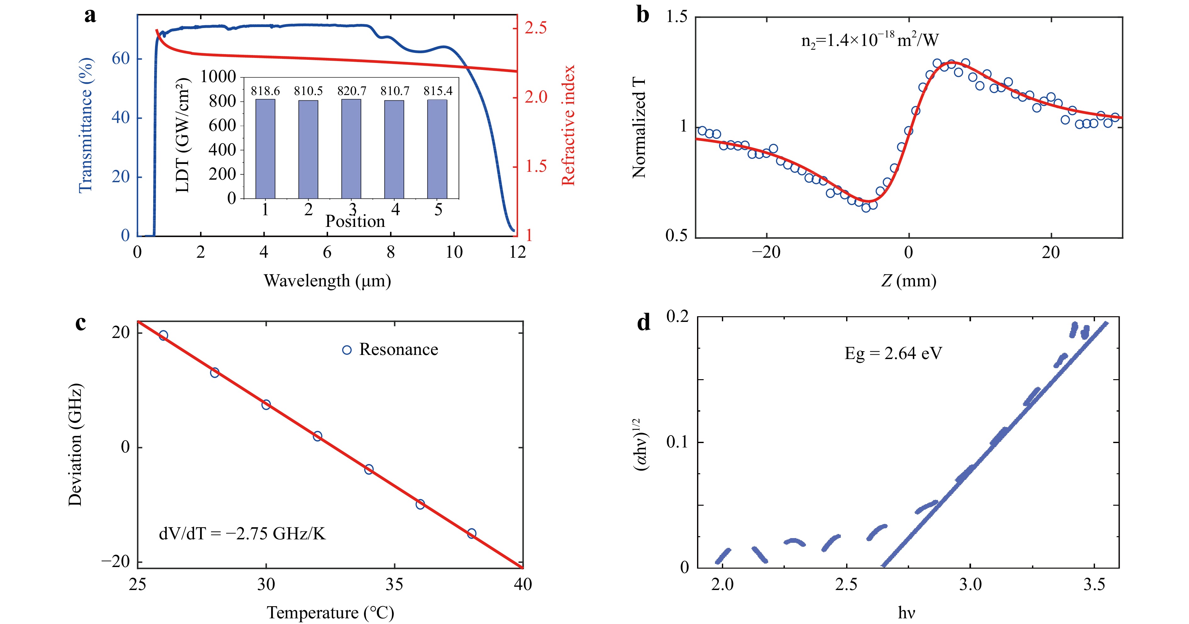
Fig. 1 Optical properties of GeSbS materials. Adapted with permission from Ref. 34, copyright 2022, WILEY. a Measured transmission window and refractive index of a GeSbS bulk material. Inset: Measured LDT at five different positions of the film. b Z-scan (close aperture) trace for determining the nonlinear refractive index of a GeSbS film. c Measured resonance frequency shift versus temperature for determining the thermo-optic coefficient (TOC) of a GeSbS resonator. d Measured Tauc’s plot for determining the bandgap of the GeSbS film.
In this article, we review recent advances in the optimised fabrication of new GeSbS-integrated devices and their applications based on their prominent Kerr nonlinearity and the photoelastic effect. We developed a modified ChG waveguide fabrication process compatible with silicon photonics integration that leverages higher quality (Q) factors (more than 5×10⁶) with respect to state-of-the-art ChG-based microring resonators34. Furthermore, based on the high nonlinearity and photoelastic coefficient of GeSbS, we experimentally demonstrated the integrated soliton microcombs and acousto-optic (AO) modulators in improved ChG-integrated devices.
-
Low-propagation-loss photonic integrated devices are crucial in various photonic applications such as low-threshold frequency combs34,36, optical signal processing18,37, and on-chip lasers38,39. Since they increase the scattering of light confined in devices, surface and sidewall roughness are crucial for realising low-loss photonic integrated devices40. By optimising thermal annealing and dry etching processes, we developed an improved fabrication method for ChG photonic integrated devices to minimise the surface roughnesses of both top and sidewalls34.
ChG thin films are typically prepared using thermal evaporation at a low temperature (Tg), through which amorphous ChGs can directly adhere to silicon substrates41, free of the wafer-bonding process12,42. This process is simple and low-cost and allows the film to be easily controlled43. A GeSbS film was deposited on a 4-inch silicon wafer using an optimised thermal evaporation technique at a low temperature (350 °C) (Fig. 2a). The uniformity of the film thickness and refractive index was characterised on a 4-inch GeSbS wafer (Fig. 2b, c). There were fluctuations in the thickness (≈ ±6.5 nm) and refractive index (≈ ±0.0075) of the film, and it had a thickness of 850 nm. However, since these fluctuations were small, they did not affect the application of this wafer in on-chip photonic integrated circuits. Then, a thermal annealing process was directly performed to reduce the surface roughness and improve the optical quality of the GeSbS film30,34,38. The effect of different annealing temperatures on the surfaces of the films were explored, including the as-deposited and thermal annealed states at 300, 350, and 400 °C. After thermal annealing at 350 °C, the RMS roughness of the GeSbS film significantly decreased from 0.623 nm for the as-deposited film to 0.241 nm34 (Fig. 2d). Annealing can cause changes in the density and molecular structure of ChGs, leading to an increase in the film thickness (less than 10 nm) and a decrease in the refractive index (less than 0.08) for films with a thickness of 850 nm. Considering the minimal changes in surface roughness at 400 °C, 350 °C was selected as the optimal thermal annealing temperature.
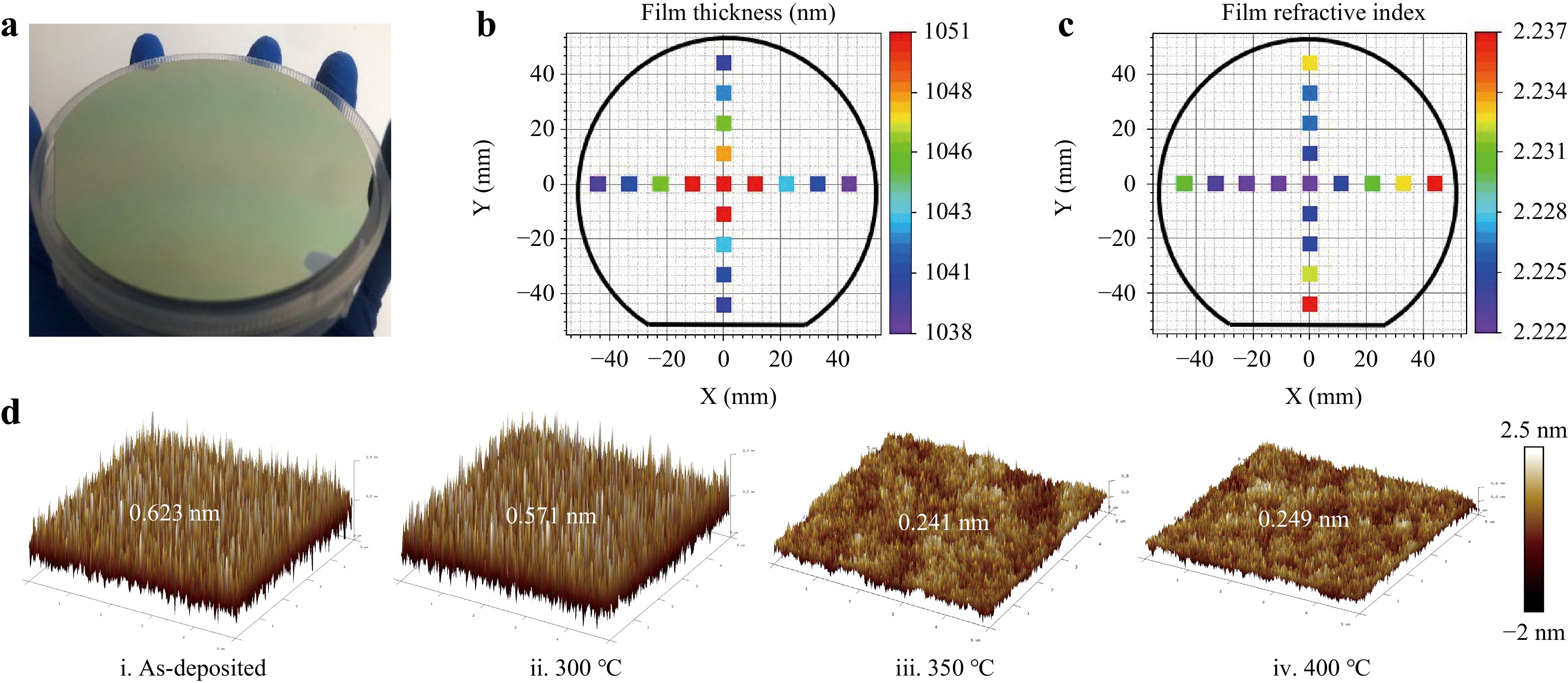
Fig. 2 Characterisation of the GeSbS film. Adapted with permission from Ref. 34, copyright 2023, WILEY. a The 4-inch GeSbS film wafer. b Thickness mapping and c refractive index mapping of a 4-inch GeSbS wafer. d Atomic force microscopy (AFM) images of GeSbS thin films in a 5 × 5 μm2 area: i As-deposited and after thermal-annealing at ii 300, iii 350, and iv 400 °C.
Subsequently, the dry-etching process was optimised to reduce the roughness of the sidewalls and improve the verticality of the waveguides. Here, the CF4/CHF3/Ar gas-based ICP-RIE etching process was modified by adjusting the flow rates of O2 and CF4 gases to reduce the scattering losses caused by in situ polymer deposition on the waveguide sidewalls (Fig. 3a, b)34. A vertical sidewall can also be achieved through an improved etching process, which is critical for the precise dispersion engineering of waveguides (Fig. 3c). Additionally, the coupling conditions of the microresonator could be finely controlled by carefully designing the width of the bus waveguide, coupling gap, and coupling length. For instance, a GeSbS microresonator with an integrated pulley bus waveguide was finely fabricated with a 500-nm target coupling gap and good verticality (Fig. 3d−f).
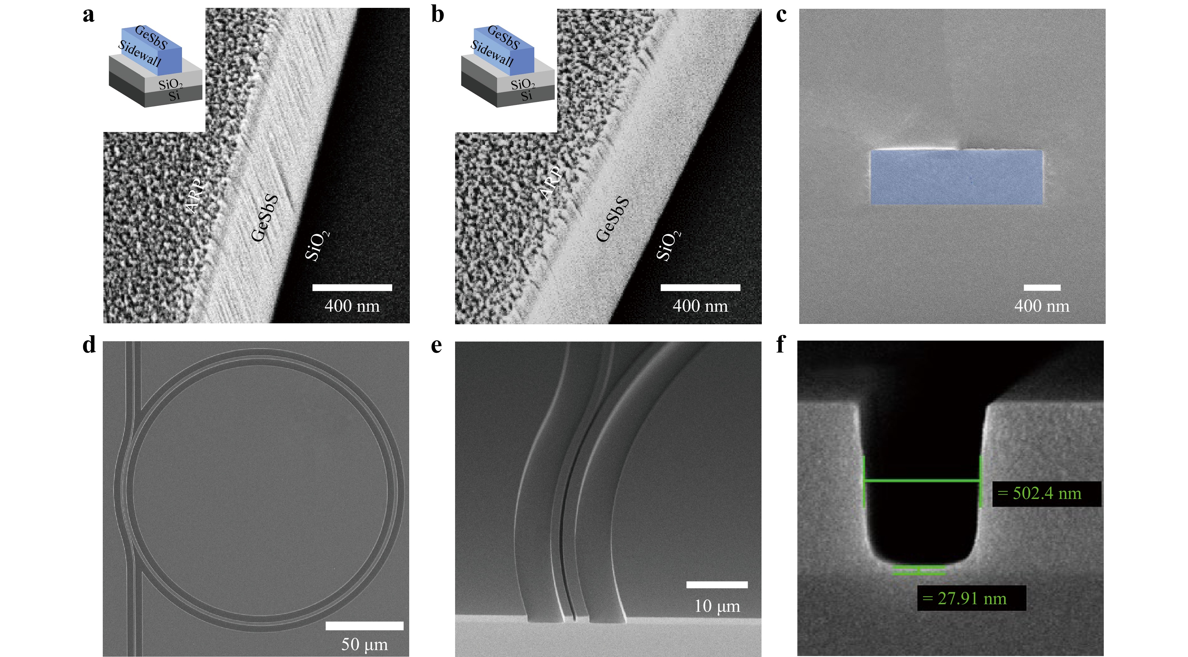
Fig. 3 Scanning electron microscopy (SEM) images of the fabricated device. Adapted with permission from Ref. 34, copyright 2023, WILEY. a, b The sidewall of the waveguides before and after the improved dry etching process. Inset: The schematic of the waveguide structure; c the cross-section with a silica cladding; d a GeSbS microresonator with a radius of 100 μm with an integrated pulley bus waveguide; e the pulley coupling region and f the cross-section for the etching width of 500 nm. The cross-section of the microresonator is 2.4 × 0.8 μm.
We have proposed a complete fabrication process for low-loss ChG-integrated devices, through which a 1× 2 cm GeSbS photonic chip can be obtained (Fig. 4a, b). Initially, GeSbS bulk glass was synthesised from high-purity elements using a mature melt-quenching technique and further purified using an improved physical and chemical purification method44. Secondly, the high-purity GeSbS, which was the deposition material source, was thermally deposited on a silicon wafer with a 3-μm SiO2 layer, followed by thermal annealing under an inert atmosphere. Then, the pattern was imprinted on the mask layer using electron-beam lithography (EBL). After development, a thermal reflow process was applied to remove the roughness of the pattern sidewalls. Next, CF4/CHF3/Ar gas-based inductively coupled plasma reactive ion etching (ICP-RIE) was used to transfer the pattern onto the GeSbS layer. Finally, a 3-μm silica layer was deposited on the top as cladding by inductively coupled plasma chemical vapour deposition (ICP-CVD). Two microresonators with typical free spectral ranges (FSR) of 200 and 6.9 GHz were fabricated using the abovementioned fabrication process. For the microresonator with a FSR of 200 GHz shown in Fig. 4c−e, a typical resonant-loaded linewidth of ≈56 MHz was measured in the critical coupling regime using the spectral scanning method, indicating an intrinsic Q-factor of 3.43 × 10⁶. The mean intrinsic Q-factor of the TE00 mode was ≈ 1.80 × 10⁶. For the microresonator with a FSR of 6.9 GHz shown in Fig. 4f−h, the measured intrinsic Q-factor of the TE00 mode was as high as 6.48 × 10⁶, and the average intrinsic Q-factor was ≈ 2.36 × 10⁶. Furthermore, the Q factor of the microresonator was insensitive to the wavelength, exhibiting a low loss over a wide range in the communication band (Fig. 4e, h).
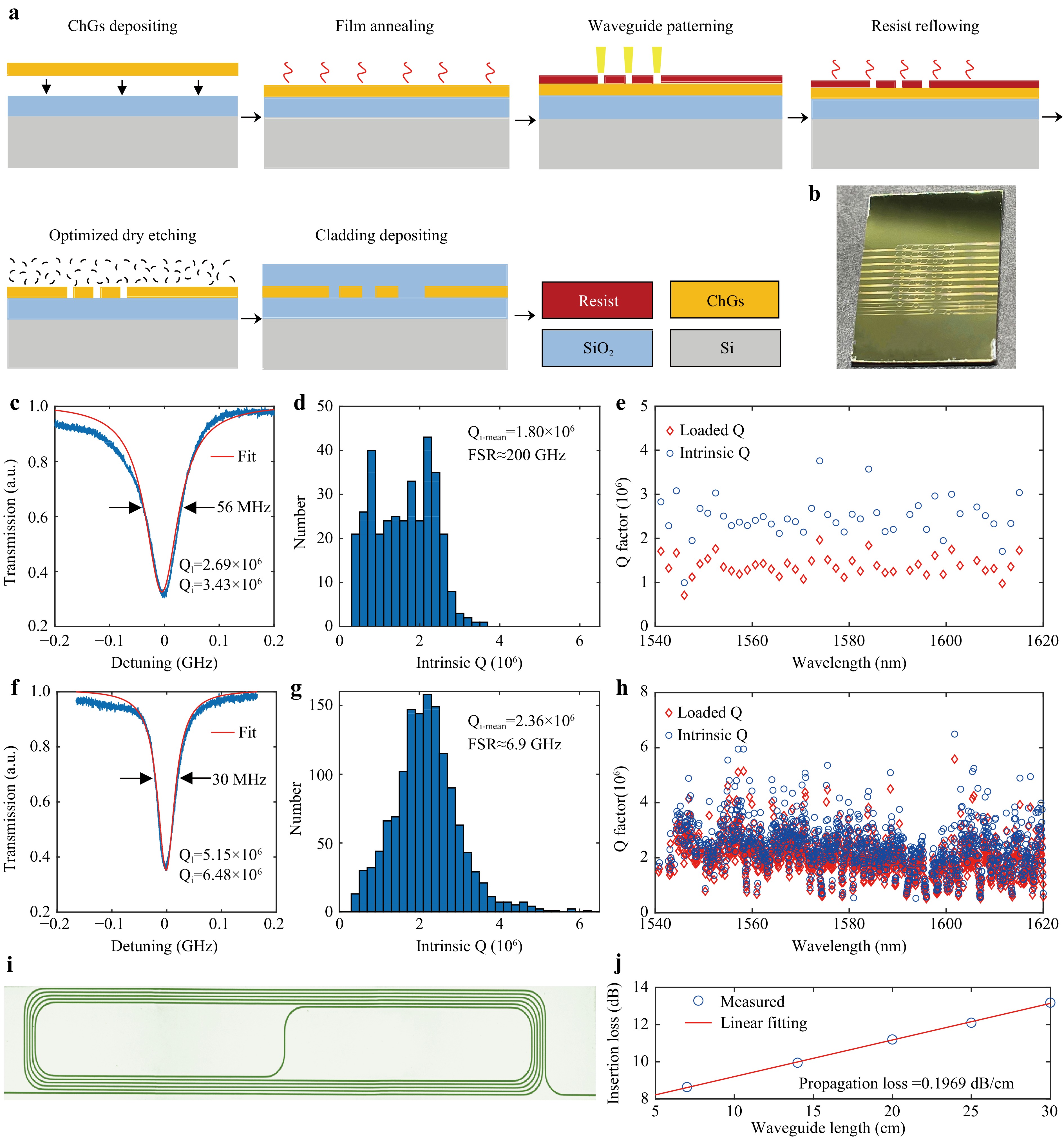
Fig. 4 Fabrication and characterisation of high-performance ChG photonic integrated devices. Adapted with permission from Ref. 34, copyright 2023, WILEY. a Fabrication process of high-performance ChG photonic integrated devices. b A photograph of a fabricated 1 × 2 cm GeSbS photonic chip. c, f The measured transmission spectra of the TE00 mode and the corresponding Lorentzian fits of two microresonators with FSR ≈ 200 and 6.9 GHz, respectively. d, g Histograms of intrinsic Q-factors. e, h Wavelength dependence of the loaded Q-factor and intrinsic Q-factor of the TE00 mode from 1540–1620 nm. i Optical micrograph of a GeSbS spiral waveguide. j Measured insertion losses of GeSbS spiral waveguides.
Our modified fabrication technology can also meet the requirements of some integrated nonlinear applications, such as integrated travelling-wave parametric amplifiers45,46 and stimulated Brillouin scattering (SBS) filters47,48, which require nearly metre-long photonic circuits. We fabricated spiral waveguides with different lengths (7, 14, 20, 25, and 30 cm) using the proposed fabrication process. An optical micrograph of a spiral waveguide with a length of 7 cm is shown in Fig. 4i. The insertion loss was measured, and a transmission loss as low as 0.2 dB/cm was obtained by linear fitting (Fig. 4j). As shown in Tables 1 and 2, we compared the losses of the microresonators and waveguides reported in previous studies using different ChG materials and methods. The results indicated that our GeSbS photonic integrated devices achieved the highest Q-factor and lowest optical loss among those of the state-of-the-art ChG microrings and planar waveguides used for comparison (order of tens of centimetres).
Material Fabrication method Wavelength (μm) Dimension (width×height) (μm) Q-factor Ref As2S3 microresonator Trapezoidal-TE 1.55 10 × 1.3 1.44 × 10⁷ 41 As2Se3 microdisk TE, Lift-off 5.2 2.5 × 1.1 2 × 10⁵ 49 Ge28Sb12Se60 microdisk TE, ICP 1.55 1 (height) 5 × 10⁵ 50 Ge11.5As24Se64.5 microdisk TE, RIE 1.55 1 (height) 1.1 × 10⁶ 51 Ge23Sb7S70 microdisk TE, RIE 1.55 0.8 × 0.45 1.2 × 10⁶ 52 Ge28Sb12Se60 microring TE, ICP 1.55 0.3 (height) 4.1 × 10⁵ 53 As20S80 microring Micro-trench, EBE 1.55 2.0 ×1.5 6 × 10⁵ 54 Ge25Sb10S65 microring TE, ICP-RIE 1.55 2.4 × 0.8 1.97 × 10⁶ 38 Ge25Sb10S65 microring TE, ICP-RIE 1.55 2.4 × 0.8 2.2 × 10⁶ 34 Ge25Sb10S65 microring TE, ICP-RIE 1.55 2.4 × 0.85 6.48 × 10⁶ This work TE: thermal evaporation; ICP: inductively coupled plasma; RIE: reactive ion etching; EBE: electron beam evaporation. Table 1. Fabrication method, working wavelength, dimensions, and Q-factors of several typical chalcogenide microresonators
Material Fabrication method Wavelength (μm) Dimension (width×height×length) Propagation loss Ref Ge11.5As24Se64.5 TE, ICP-RIE 1.55 0.63 μm × 0.5 μm × 0.18 cm 2.6 dB/cm 55 Ge23Sb7S70 TE, RIE 1.55 0.8 μm × 0.42 μm × 1 cm 0.5 dB/cm 56 Ge11.5As24Se64.5 TE, ICP 3 - 5 4 μm × 2.5 μm × 1.4 cm ~0.5 dB/cm 57 Ge11.5As24Se64.5 TE, ICP 3.8 - 5 4.0 μm × 4.4 μm × 1.8 cm ~0.6 dB/cm 27 As2S3 TE, ICP 2 1.2 μm × 0.6 μm × 2.4 cm 1.45 dB/cm 58 As2Se3 TE, wet etching 8.4 5.4 μm × 4.53 μm× 3.55 cm 0.5 dB/cm 59 As2Se3 Sputter, Lift-off 3.5 10 μm × 1 μm × 5 cm 0.16 dB/cm 60 Ge25Sb10S65 TE, ICP-RIE 1.55 2.5 μm × 0.7 μm × 30 cm 0.2 dB/cm This work TE: Thermal evaporation; ICP: inductive coupled plasma; RIE: reactive ion etching. Table 2. Fabrication method, working wavelengths, dimensions, and propagation losses of several typical chalcogenide waveguides
-
Mode-locked optical frequency combs have revolutionised a wide variety of applications including optical atomic clocks61-64, coherent communication systems65-69, microwave and optical frequency synthesis1,70, molecular footprint detection71-75 and light detection and ranging (LiDAR)76,77. In particular, integrated frequency combs based on Kerr nonlinear microresonators (microcombs) are an attractive choice for realising frequency comb sources with a high coherence, chip-scale sizes, and low power consumption at the milliwatt level78,79. In recent decades, dissipative Kerr soliton microcombs have been demonstrated in various photonic integrated platforms, greatly promoting the development of nonlinear optics and supporting new developments in microcomb applications. In contrast, there is motivation to shift focus from exploring telecommunication bands to seeking new materials for simultaneously realising ultrahigh nonlinear efficiencies based on both material nonlinearities and high Q factors, as well as new broadband spectral windows. Microcombs have been demonstrated in the mid infrared (MIR) bands of silicon and Si3N4 microresonators80,81; the spectral windows of more than 4 μm in these microcombs are currently limited by the SiO2 substrate and cladding of the current platforms8. Additionally, there were no reports of optical frequency combs based on ChG photonic devices till the development of GeSbSs. We conducted a series of studies on the generation and manipulation of microcombs based on GeSbS microresonators.
-
Precise dispersion engineering and high Q factors strongly support the role of microresonators in the generation of third-order nonlinear optical processes and Kerr microcombs. The dispersion of GeSbS microresonators was tailored using geometric parameters and theoretically calculated using the finite element method. The integrated dispersion Dint can be used to characterise the full-order dispersion of GeSbS microresonators; this parameter can be defined as82:
$$ {D}_{int}={\omega }_{\mu }-{\omega }_{0}-{D}_{1}\mu =\frac{{D}_{2}{\mu }^{2}}{2!}+\frac{{D}_{3}{\mu }^{3}}{3!}+\sum _{m > 3}\frac{{D}_{m}{\mu }^{m}}{m!} $$ (1) where μ and ωμ are the relative mode numbers and angular frequencies of the resonances, respectively; D1/2π is the FSR; D2 is the second-order microresonator dispersion; and D3 is the third-order microresonator dispersion. The measured integrated dispersion curves were characterised by calibrating the resonant frequency of the microresonators using a fibre-based Mach-Zehnder interferometer (MZI) and removing the offset frequency and linear dispersion term, which were consistent with the simulation results (Fig. 5a, b). The second-order dispersions were calculated to be −8.2 and 2.1 MHz for the TE00 mode and TM00 mode, respectively, in the GeSbS microresonators with a radius of 100 μm and a cross-section of 2.4 × 0.8 μm (width × height).
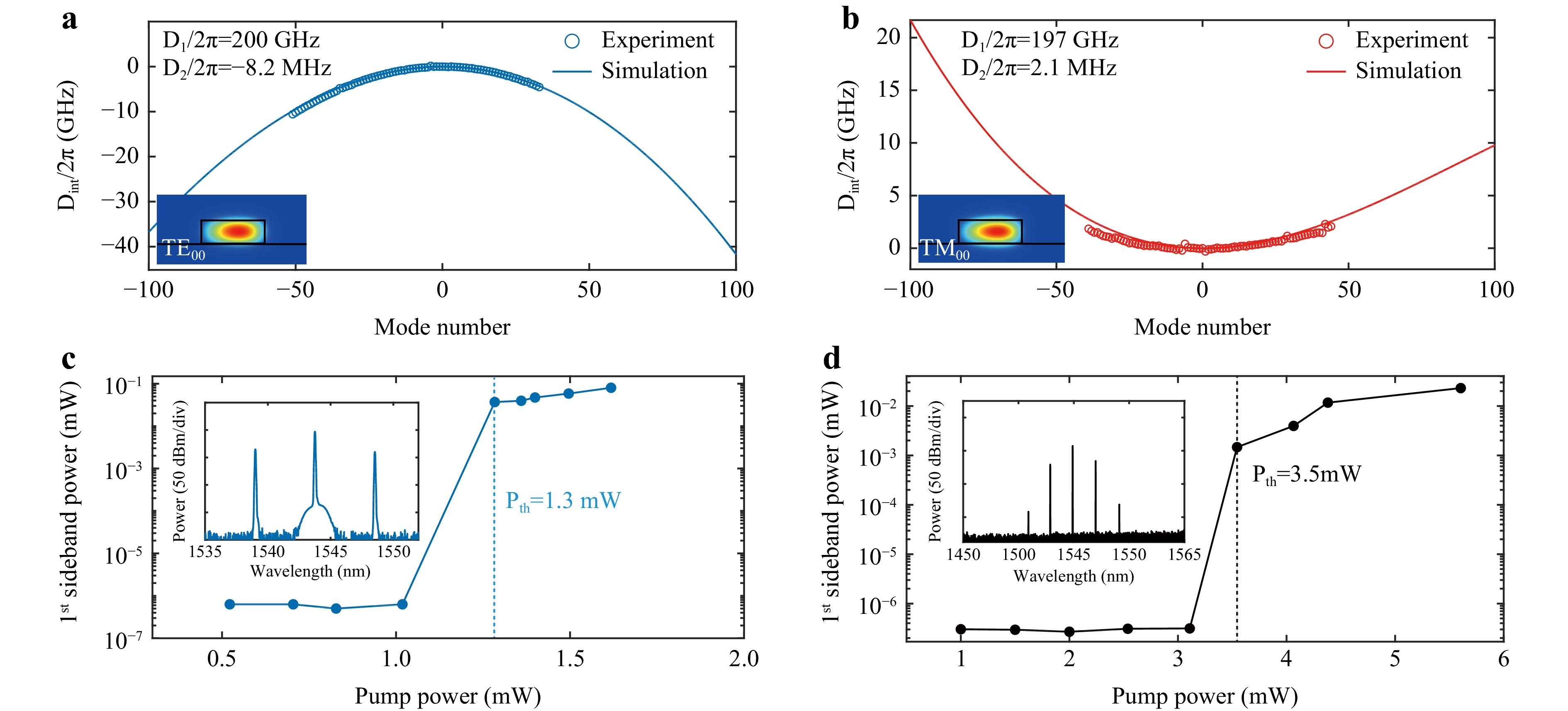
Fig. 5 Dispersion engineering of the two orthogonal polarization fundamental modes in the high-Q microresonator and low threshold OPO generation. Adapted with permission from Ref. 34, copyright 2023, WILEY. a, b The calculated and measured integrated dispersion (Dint) values for the TE00 and TM00 modes with a radius of 100 μm and a cross-section of 2.4 × 0.8 μm (width × height). The second-order dispersions (D2/2π) are −8.2 MHz (normal dispersion) and 2.1 MHz (anomalous dispersion). The insets are the optical field distributions in the cross-section. c, d The pump power dependence of the 1st OPO sideband, revealing low power thresholds of 1.3 and 3.5 mW. The insets are the experimentally measured output power spectra of the OPO sidebands.
The threshold of optical parametric oscillation is estimated by34:
$$ {P}_{th}=\frac{\pi }{8}\frac{n}{{n}_{2}}\frac{{v}_{0}}{{v}_{FSR}}\frac{{A}_{eff}}{{Q}_{i}^{2}}\frac{{\left(1+{\textit κ} \right)}^{3}}{{\textit κ} } $$ (2) where n is the linear refractive index; n2 is the nonlinear refractive index; v0 is the pump frequency; vFSR is the FSR of the microresonator; Aeff is the effective mode area of the microresonator; and the coupling factor κ = κex/κi, where κex is the coupling rate, and κi is the intrinsic rate of the microresonator. The extract intrinsic Q-factors of the fabricated microresonators were 1.6 × 10⁶ and 2.3 × 10⁶ for the TM00 and TE00 modes, respectively, contributing to lower power requirements for triggering the OPO. The pump thresholds for the TM00 and TE00 modes were 1.3 and 3.5 mW, respectively, as measured by the power dependence of the generated first-order FWM sidebands with the input pump power (Fig. 5c, d).
-
Owing to the distinct dispersion characteristics of the two fundamental polarised modes in the GeSbS microresonator, bright soliton and dark-pulse microcombs could be achieved in a single GeSbS microresonator, as shown in Fig. 6a. With an input power of ~ 20 mW, a bright dissipative Kerr microcomb was experimentally obtained by pumping the TM00 mode family, which featured a broad spectrum ranging from 1440 to 1680 nm and a comb repetition rate of 197 GHz, as shown in Fig. 6b. Due to the low thermo-optic coefficient (TOC) (e.g., dn/dT ≈ 3.1 × 10⁻⁵ K−1) of GeSbS, the soliton microcomb could be stably captured by manually sweeping the pump frequency from blue detuning to red detuning without any complicated pumping schemes79,83-88. Moreover, a dark-pulse microcomb assisted by the avoided mode-crossing effect (AMX) was demonstrated in the same microresonator. In general, the origin of the AMX is the multimode nature of ChG microresonators and random fabrication imperfections, which cause linear coupling between different mode families. Only ~ 25 mW of input power was used to drive the dark-pulse microcomb with a microcomb bandwidth of 80 nm (1510–1590 nm) and a repetition rate of 200 GHz, as shown in Fig. 6d. The low pump power requirements of both microcomb generations facilitated the full integration of our chip with commercial on-chip DFB lasers. Furthermore, the formation of dissipative solitons could dramatically reduce the comb intensity noise, as shown in the radio frequency (RF) spectra collected from the electrical spectrum analyser (ESA) in Fig. 6c, e. In combination with well-developed self-injection-locking technologies, the performance of versatile bright and dark soliton microcombs generated in GeSbS microresonators may be further improved and operated in a turnkey scheme, which is favourable for practical applications36, 78, 89, 90.
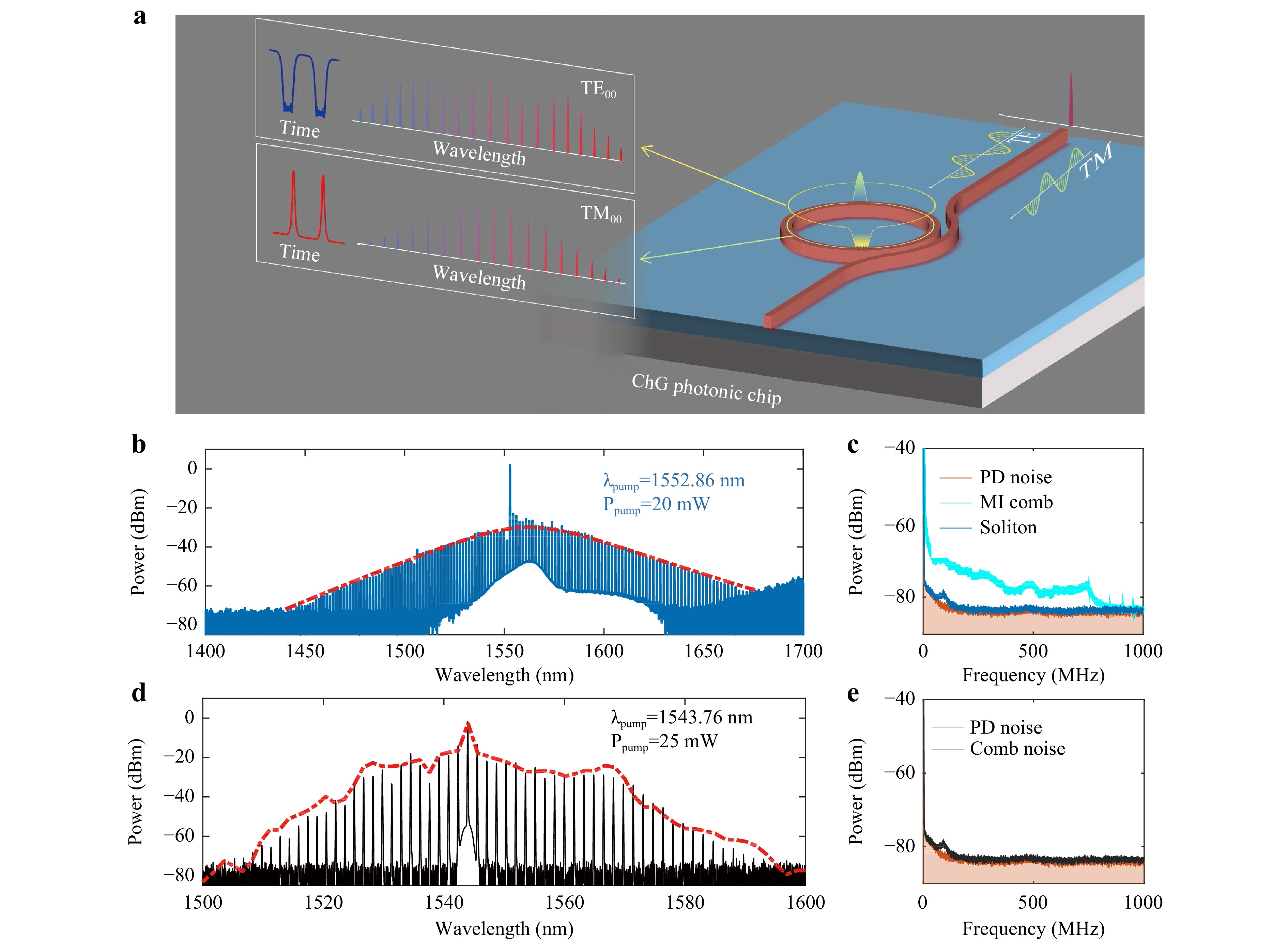
Fig. 6 Low-power bright and dark soliton microcombs based on integrated GeSbS microresonators. Adapted with permission from Ref. 34, copyright 2023, WILEY. a Schematic illustration of soliton microcomb generations in an integrated ChG microresonator, including a dark-pulse soliton in the TE00 mode and a bright soliton in the TM00 mode. b, d Output power spectra as the pump frequency sweeps across the resonances, with the soliton transition steps. c, e Experimental output optical spectra of a bright soliton in TM00 mode families and a dark-pulse microcomb in TE00 mode families.
-
We also systematically studied the interplay between stimulated Raman scattering (SRS) and the Kerr nonlinear process of GeSbS microresonators (Fig. 7a, b)38. Owing to the broadband Raman gain spectra of GeSbS materials38, the significant Raman effect affects the formation of Kerr microcombs, especially in the weak anomalous dispersion and normal dispersion regime91,92. The underlying physical mechanism that mediates the nonlinear interaction of Raman lasers and Kerr combs can be attributed to the degenerate FWM process among the pump, Stokes, and second-order Stokes resonant modes and the nondegenerate FWM process involving the pump wave, first and second Stokes waves, and anti-Stokes wave, as shown in Fig. 7c. If the cavity dispersion of a microresonator is improperly designed, it results in large frequency mismatching ($ \mathrm{\Delta }v $) among the three participant resonant modes, which hinders the efficiency of the FWM process and results in the cascading of stimulated Raman scattering (SRS) (Fig.7d). Consequently, the spontaneous FWM process dominates and leads to the formation of Raman-Kerr frequency combs. Otherwise, if the frequency mismatch is sufficiently small, the cascading of SRS occurs93-96. Therefore, a broadband Raman-Kerr microcomb spanning 1450–1700 nm was obtained in the GeSbS microresonators by pumping with an input power of 30 mW, as shown in Fig. 7e. A broadband Raman gain of approximately 1630 nm simultaneously extended the spectral range and enhanced the comb power, providing potential high-power microcomb sources for molecular spectroscopy. The results provided a clear insight into the Kerr-Raman nonlinear effect in integrated ChG microresonators and showed that using this effect was a viable approach for future Kerr microcombs in the near-IR and MIR regions.
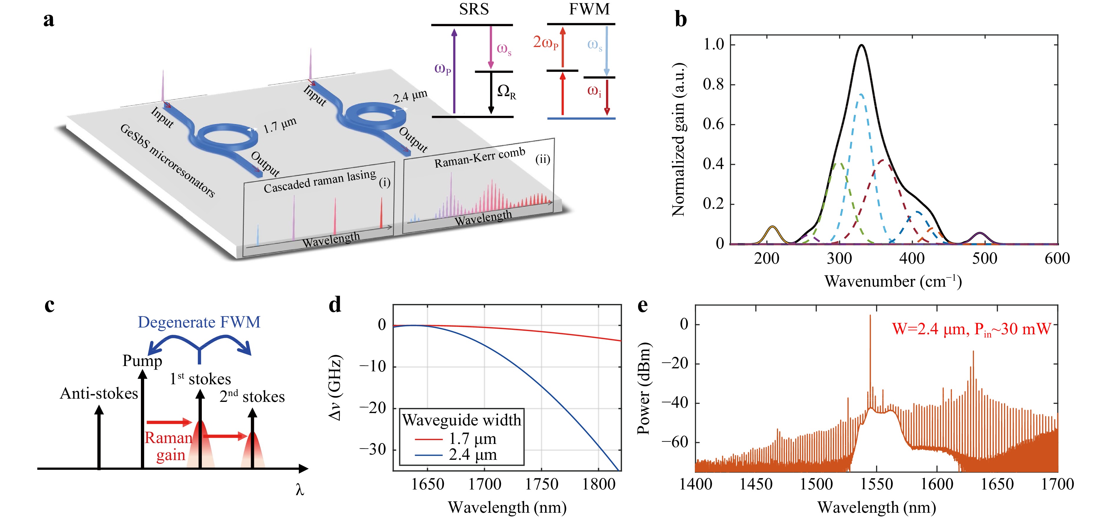
Fig. 7 Broadband Raman-Kerr comb in GeSbS microresonators. Adapted with permission from Ref. 38, copyright 2022, WILEY. a A schematic of engineered Raman lasing in GeSbS microresonators. b Raman response spectrum of a GeSbS film. c Schematic diagram of the degenerate four-wave mixing (dFWM) between a pump wave and the first- and second-order Stokes waves. d Calculated phase mismatch curves for the TE00 mode of two microresonators with microresonator widths of 1.7 and 2.4 μm. The film thickness is fixed at 0.8 μm. e Measured broadband Raman-Kerr comb in the GeSbS microresonator with a width of 2.4 μm.
-
An octave-spanning microcomb enables an f-2f self-reference scheme to completely stabilise the optical frequency comb, which is critical for timing, metrology, and molecular applications11, 62, 97, 98. Soliton Cherenkov radiation or dispersive wave (DW) emission is a key route for reliably extending the bandwidths of optical frequency combs in photonic integrated microresonators62. Generally, in the absence of third- and higher-order dispersions, a soliton microcomb spectrum features a smooth sech2 envelope corresponding to a bright soliton pulse in the time domain. In a small group velocity dispersion (GVD) region, the higher-order dispersion dominates the second-order dispersion, leading to the reshaping of the microcomb spectrum. The pump power can be efficiently transferred to comb lines far from the pump frequency if the phase-matching condition is satisfied. Considering the integrated dispersion in microresonators, the generation of DWs is spectrally located at Dint = 082. Currently, broadband microcombs, especially those with DWs, suffer from the deterioration of comb spectral flatness owing to the large phase mismatch in certain spectral ranges99. Mode hybridisation in waveguides and microresonators has enabled advanced dispersion engineering through fine geometrical tuning, which has been utilised for bright soliton microcombs in normal-dispersion Si3N4 microresonators100 and two-colour soliton microcomb generation101,102. Thus, to further extend the bandwidths and flatten the spectra of microcombs, we propose a GeSbS microresonator with dual-ring microresonators (DRMs) to optimise microcavity dispersion over a wide spectral range using mode hybridisation (Fig. 8a)99. We systematically investigated arbitrary dispersion shaping at specific wavebands and engineered octave frequency combs based on mode hybridisation in mutually coupled concentric microresonators99. When the optical path lengths (OPL) of the inner and outer microresonators were equal, the eigenfrequencies of the antisymmetric supermode in the DRMs were shifted owing to mode hybridisation, generating a new local anomalous dispersion window in the strong normal dispersion region. As a result, an octave-spanning Kerr soliton microcomb with multidispersive waves was numerically achieved with an input power of 40 mW based on the Lugiato-Lefever equation (LLE)103-105, covering wavelengths from 1224 to 2913 nm, as shown in Fig. 8b. The FSR of the dual-ring microresonator was approximately 620 GHz. Moreover, the number of comb lines within the bandwidth of −40 dB could reach 126, and the total comb power was ~ 1.7 mW. The integrated dispersion profile can be flattened over a broadband wavelength range by tailoring the geometric parameters of DRMs. The flexible structures of DRMs enhance the dynamics of frequency combs in GeSbS platforms and enable the generation of octave soliton microcombs with dispersion-engineered multiple-dispersive waves.
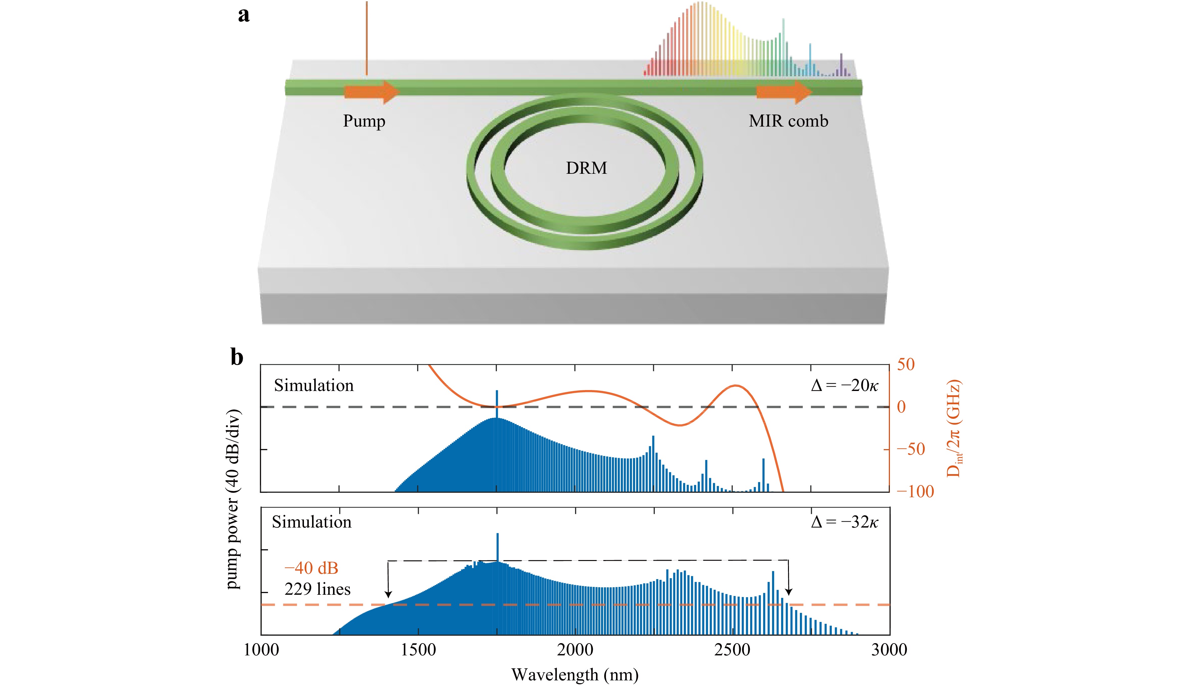
Fig. 8 Broadband microcomb generation in dispersion-engineered chalcogenide dual-ring microresonators. Adapted with permission from Ref. 99, copyright 2023, FRONTIERS. a Schematic of a dual-ring microresonator. b A microcomb with multiple dispersive waves at a red detuning of −20 κ (Upper panel) and a beyond-octave microcomb at a detuning of −32 κ (Lower panel) in the DRMs.
-
Regarding AO modulators, they enable the manipulation of confined photons in photonic materials through the tuning of the refractive indices of the materials using radio frequency (RF)-driven acoustic waves106,107. Traditional AO devices based on bulk materials suffer from weak light and acoustic wave confinement, which leads to AO modulators having high pump powers108. Surface acoustic waves (SAWs) can be well-confined near photonic integrated circuits (PICs), such as integrated waveguides and microresonators, and exhibit a high-energy overlap within a wavelength-scale chip109,110. Thin-film lithium niobate (TFLN) has attracted increasing interest for the realisation of high-performance AO modulators in PICs, owing to its superior advantages in electro-optical conversion, including a strong electro-optic effect, a large refractive index, and a wide transparency wavelength111,112. However, owing to acoustic leakage, the modulation efficiencies of AO modulators become weak, which is a bottleneck in TFLN-based AO modulators. Suspended LN acoustic resonator construction is commonly used to enhance the overlap coefficient between optical and acoustic modes; this method requires strict integrated fabrication processing. Being a typical ChG, GeSbS is resistant to acidic environments and can be easily etched using alkaline reagents. Therefore, a GeSbS waveguide can be suspended by the HF etching of a SiO2 layer, enabling higher-frequency AO modulation. Indeed, suspended structures can enhance the bounds of acoustic modes and improve the AO overlap in a waveguide because optical modes in common optical-material-based waveguides can be bound by total internal reflection. However, acoustic modes can leak into substrates because the acoustic wave velocities in waveguides resemble those in the substrates, resulting in reduced AO overlaps in the waveguides113. However, GeSbS has a high refractive index and a low acoustic velocity (~2.6 km/s), allowing the high confinement of the optical and acoustic modes within a waveguide without suspended structures114,115. Thus, high-frequency (higher than 1 GHz) AO modulation can also be achieved by changing a interdigital electrode structure while preserving the current waveguide structure. Moreover, the refractive indices of Ge25Sb10S65 (n=2.23) and TFLN (ne=2.13) at 1550 nm were similar. In addition, the photoelastic coefficients of GeSbS were anisotropic, and those of p11, p12 and p44 were 0.25, 0.24 and 0.05, respectively. Therefore, we have proposed a hybrid TFLN-ChG integrated waveguide, which benefits from the electrical, optical, and material advanced properties of TFLN and ChG thin films, for high-efficiency integrated AO modulators24,116.
We extracted the Vπ of an AO modulator to quantitatively evaluate the AO modulation characteristics based on non-suspended TFLN-ChG MZIs from a measured opto-acoustic S21 spectrum, as expressed through the following equation117:
$$ {V}_{\pi }=\frac{\pi {R}_{PD}{I}_{\text{rec}}}{\left|{S}_{21}\right|} $$ (3) where RPD is the sensitivity of the photoreceiver, and Irec is the DC optical power at the bias point with a π/2 phase difference between the two arms of the MZI. Amorphous ChGs have nearly two times higher photoelastic coefficients than those of TFLNs, potentially providing smaller Vπ values in TFLN-ChG waveguide-based AO devices16,118,119.
To improve the modulation efficiency, a high Q-factor microresonator with an interdigital transducer (IDT) was used to realise strong interactions between the photons and phonons (Fig. 9a, c)116. To exploit the photoelastic effect of the ChG material, we designed a ChG waveguide to confine most of the optical energy (Fig. 9b). The intensities of the three peaks at frequencies of 0.843, 0.88, and 1.464 GHz in the S21 spectrum were more than −50 dB (Fig 9d)116. As a result, the calculated Vπ was 1.74 V, corresponding to a half-wave-voltage-length product of 0.02 V·cm, which indicated that AO conversion had been enhanced at 0.843 GHz.
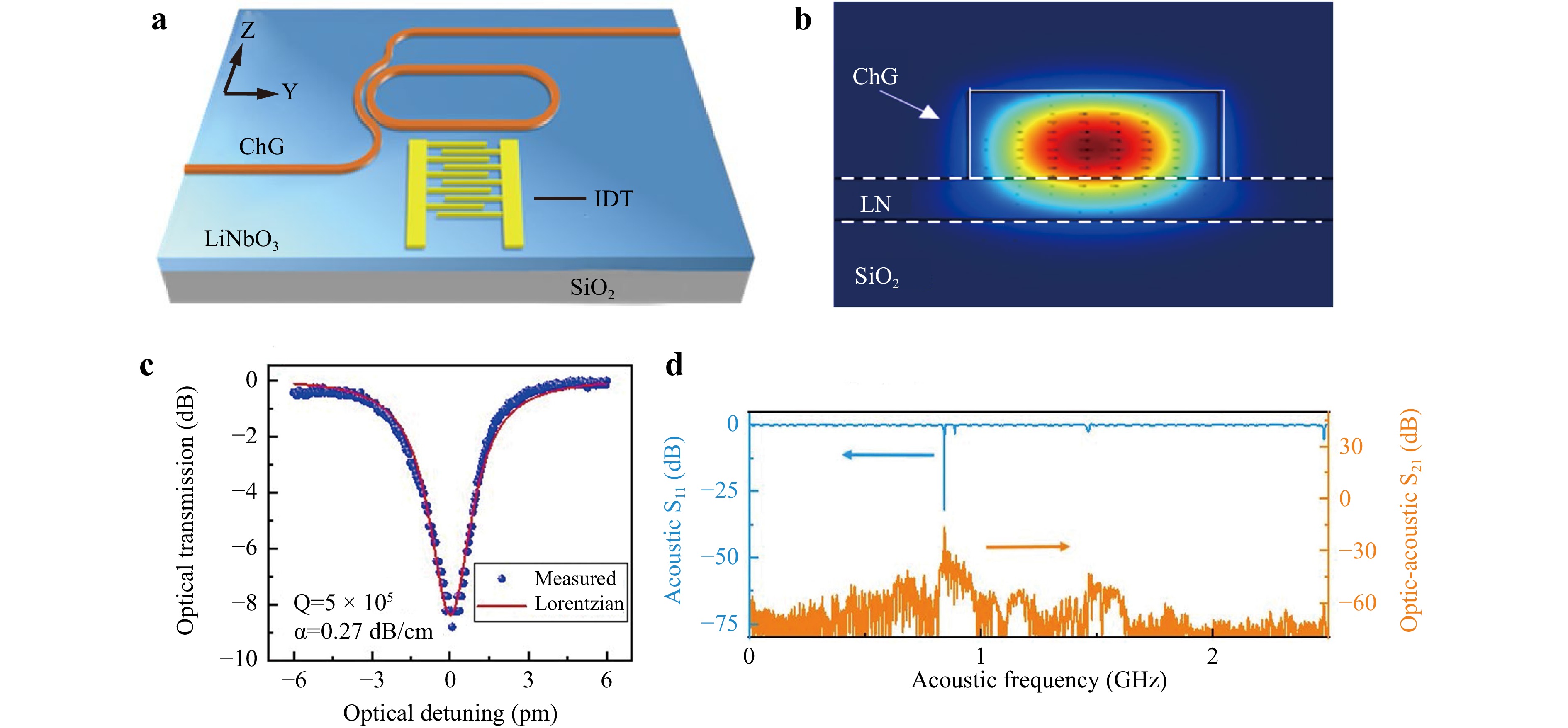
Fig. 9 Efficient AO modulation using a microring resonator on a TFLN-ChG hybrid platform. Adapted with permission from Ref. 116, copyright © The Optical Society. a Schematic of the AO modulator with microresonator modulation configurations. b Electric field of the fundamental TE mode. c Lorentz fitting (red curve) of the resonance dip at 1551.198 nm corresponding to a loaded Q-factor of 5 × 10⁵. d Acoustic S11 and S21 spectra of the AO modulators with the microresonator modulation configuration, in which the Irec amplified by EDFA is −5.6 dBm, the S21 is −16.52 dB at 0.843 GHz, and RPD is 300 V/W.
To improve the modulation efficiency of a MZI-based AO modulator consisting of waveguide arms, we further propose a built-in push-pull AO modulation structure (called a double-arm-modulated device) based on an anti-symmetric SAW mode (Fig. 10a, b). The geometric dimensions of the waveguide were optimised using an antisymmetric Rayleigh SAW (Fig. 10c, f). The optimised IDT was placed in the two waveguide arms of a MZI, which effectively utilised the energy of the acoustic waves in both directions to achieve more efficient AO modulation (Fig. 10d, e). Moreover, we concentrated approximately 83% of the optical energy in the ChG waveguides, significantly improving the AO overlap factor (Fig. 10f). As a result, in the case of a sound phase difference up to π, the modulation efficiency was twice that of the single-arm-modulated device (Fig. 10h)24.
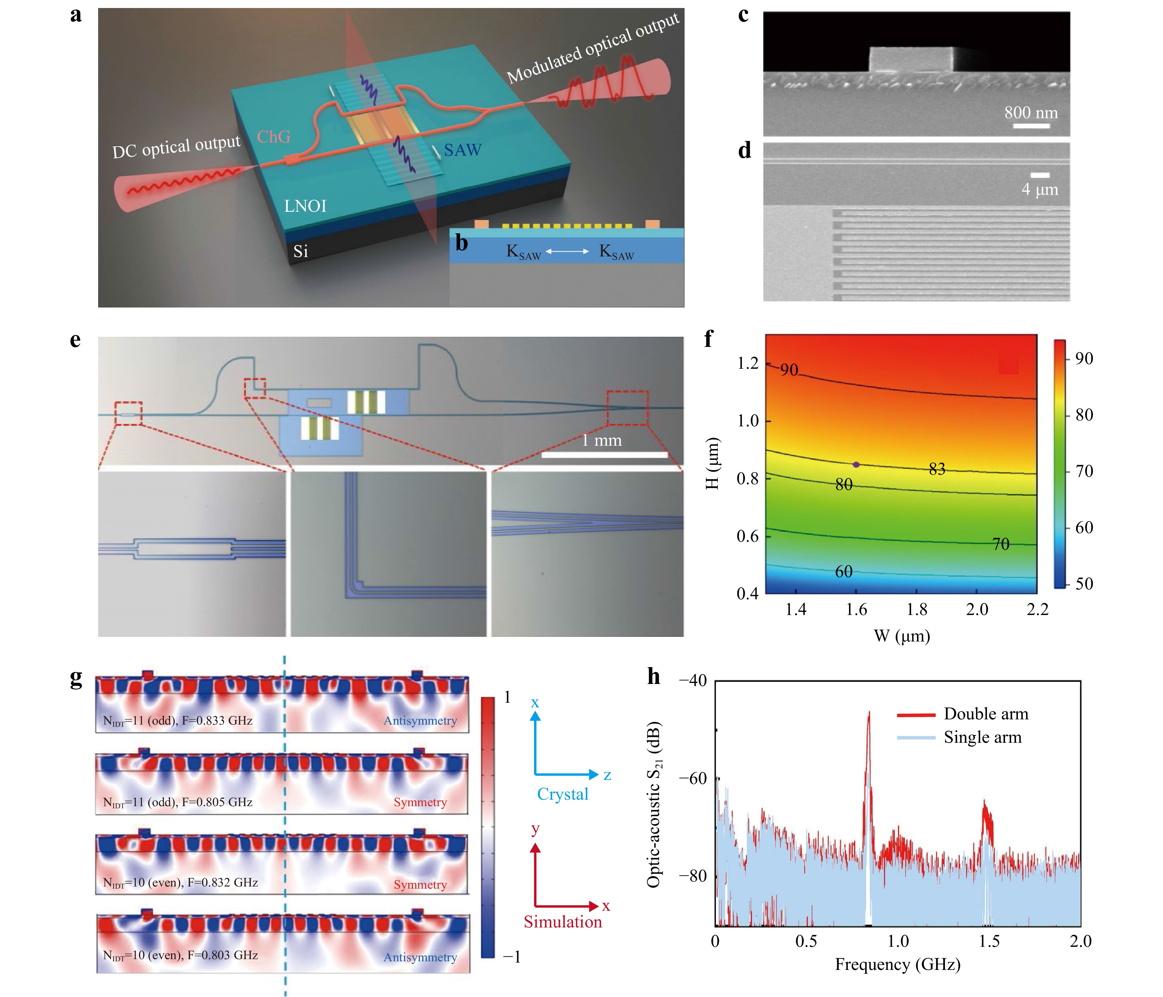
Fig. 10 Highly-efficient AO modulation using nonsuspended built-in push-pull structure. Adapted with permission from Ref. 24, copyright 2022, NPG. a Schematic diagram of the proposed device. The thickness of the TFLN is fixed at 400 nm, and the thickness of the oxide layer is 2 μm. b Cross-section image of the proposed device. c SEM image of the cross-section of the modulated waveguide. d SEM image of the modulation area, including the IDT and waveguide. e Microscopic image of a TFLN-ChG hybrid MZI-based AO modulator. f Relation between the energy confinement factor Γ in the ChG waveguide and waveguide geometry. The optimized H and W of the waveguides are chosen as 850 nm and 2.05 μm, respectively. g Numerical simulation results of the dominant Sxx strain components of the SAW modes in the heterogeneous-integration waveguide platform with the double arm modulation configuration. h S21 spectra of the TFLN-ChG hybrid MZI-based AO modulators with single-arm and double-arm modulation configurations.
By properly designing the IDT structure with odd fingers, an opposite refractive-index change can be achieved in the double-arm waveguide, maximising the conversion between the acoustic and optical waves. For instance, the SAW modes at 0.833 GHz and 0.805 GHz corresponded to 5.5 (number of fingers NIDT=11, odd) and 5 (NIDT=10, even) pairs of IDT fingers, respectively (Fig. 10g, h). Therefore, an IDT with 50.5 pairs of fingers (NIDT=101) was designed to realize the effective excitation of the SAWs. Moreover, compared to our single-arm-modulated device, the intensity of the frequency peak at 0.844 GHz in the optoacoustic S21 spectrum of the double-arm-modulated device increased by 12 dB (Fig. 10h). The modulation efficiency of the push-pull AO modulator was up to 0.03 V·cm (VπL), which was three times that of the single-arm modulation device.
We compared our AO modulators, including the single-arm-modulated and double-arm-modulated ones based on the non-suspended TFLN-ChG hybrid waveguides, with those based on the TFLN in Table 3. Our results showed the highest AO modulation efficiency based on a non-suspended TFLN waveguide. Presently, the on-chip loss of our devices was as high as 5 dB, which was mainly due to the four compact 90° bending waveguides. Additionally, AO efficiency depends on the material density120, and annealing can change the density, thereby affecting the AO coefficient. To date, we have not performed experiments to compare the AO changes before and after annealing. We plan to further optimise the device structure and fabrication process to achieve a higher AO modulation efficiency.
Platform Acoustic cavity Frequency (GHz) 1-|S11|2 (%) L (μm) αp (rad/√mW) VπL (V cm) Ref./device LNa √ 0.11 42 1200 0.073 2.5 121 As2S3/SiO2/LNa √ 0.11 95 2400 0.26 0.94 122 LNb √ 3.33 64 100 0.27 0.046 123 LNb √ 1.16 19.3 45 0.54 0.019 117 LN × 1.9 50 45 0.017 0.38 117 LN × 1.9 90 45 0.018 0.27 117 SA: Ge25Sb10S65/LN × 0.84 98.5 120 0.12 0.1 24 DA: Ge25Sb10S65/LN × 0.84 98.5 120 0.4 0.03 24 a In-plane metal grating reflectors have been fabricated to construct an acoustic cavity. b: Suspended TFLN is etched as an acoustic cavity. Table 3. Comparison of modulation metrics for TFLN MZI-based AO modulators24.
-
In this review, we have discussed recent progress in the improved fabrication of hybrid integrated ChG photonic devices and related integrated applications based on Kerr nonlinearity and the AO effect. High-Q integrated microresonators and low-loss planar waveguides were achieved through improved hybrid chip fabrication, including the preparation of a GeSbS thin film and an improved fabrication process compatible with that of silicon photonics. The advantages of low loss, high nonlinearity, superior AO interactions, and versatile Kerr microcomb interactions were demonstrated in the generation of versatile Kerr microcombs and highly-efficient integrated AO modulators.
To date, this novel hybrid ChG–silicon device is still in its early stages of development. There is ample room to apply the potential of this device in broadband spectral coverage, high nonlinearity, and photoelastic effects, as well as multifunctional hybrid or heterogeneous integration with other material platforms. The fabrication of this device should reach a point where reproducible, high-yield, and wafer-scale processing can be accomplished while increasing the Q-factor up to the material absorption limit. Moreover, low-loss ‘all-ChGs’ waveguides with both ChGs as the core and claddings need to be developed for flexible dispersion engineering and extending operating wavelengths to the MIR region. Additionally, owing to their low-temperature deposition features and compatibility with silicon photonic fabrication, integrating active materials, such as III-V materials and rare-earth elements, with ChG photonic circuits, can open up opportunities for realising narrow-linewidth lasers, on-chip amplifiers, and fully integrated microcomb sources. We believe that ChG-based photonic integration will revolutionise existing photonic applications through the development of a new class of devices in the near-IR-to-MIR spectral range.
-
This work was supported by the National Key R&D Program of China under Grant (2019YFA0706301), the Key Project in Broadband Communication and New Network of the Ministry of Science and Technology (MOST) (2018YFB1801003), the National Science Foundation of China (NSFC) (U2001601, 61975242, 61525502, 62175095, 62375292), and the Natural Science Foundation of Guangdong Province for Distinguished Young Scholars (2023B1515020028).
Hybrid-integrated chalcogenide photonics
- Light: Advanced Manufacturing 4, Article number: (2023)
- Received: 27 March 2023
- Revised: 26 July 2023
- Accepted: 27 July 2023 Published online: 22 September 2023
doi: https://doi.org/10.37188/lam.2023.024
Abstract: High-quality photonic materials are critical for promoting integrated photonic devices with broad bandwidths, high efficiencies, and flexibilities for high-volume chip-scale fabrication. Recently, we designed a home-developed chalcogenide glass (ChG)-Ge25Sb10S65 (GeSbS) for optical information processing chips and systems, which featured an ultrabroad transmission window, a high Kerr nonlinearity and photoelastic coefficient, and compatibility with the photonic hybrid integration technology of silicon photonics. Chip-integrated GeSbS microresonators and microresonator arrays with high quality factors and lithographically controlled fine structures were fabricated using a modified nanofabrication process. Moreover, considering the high Kerr nonlinearity and photoelastic effect of ChGs, we realised a novel ChG hybrid integrated chip, inspired by recent advances in integrated soliton microcombs and acousto-optic (AO) modulators.
Research Summary
Hybrid-integrated chalcogenide photonics: recent breakthroughs and opportunities
Multifunctional photonic integrated chips, inspired by the hybrid and heterogeneous integration of various materials, have achieved unique optoelectronic properties by precisely controlling the structure of materials and their interaction with the optical field at the chipscale. Chalcogenide glasses (ChGs) are promising candidates for Highly efficient nonlinear photonics and acousto-optic modulator devices due to their broadband transmittance window, high nonlinearity and photoelastic coefficient. Bin Zhang from Sun-Yat Sen University and colleagues, carefully reviewed their recent advancements in the development of integrated ChG photonic chips with ultralow optical losses and the applications of these chips in nonlinear photodevices and acousto-optic modulators. These advancements have effectively addressed key issues such as improving the nonlinear interaction within highly confined waveguides and efficiently modulating heterogeneously integrated optical waveguides using surface acoustic waves. These results demonstrate that ChG-based photonics devices offer new opportunities for achieving higher levels of integration, larger bandwidths, and lower power consumption in photonic chips.
Rights and permissions
Open Access This article is licensed under a Creative Commons Attribution 4.0 International License, which permits use, sharing, adaptation, distribution and reproduction in any medium or format, as long as you give appropriate credit to the original author(s) and the source, provide a link to the Creative Commons license, and indicate if changes were made. The images or other third party material in this article are included in the article′s Creative Commons license, unless indicated otherwise in a credit line to the material. If material is not included in the article′s Creative Commons license and your intended use is not permitted by statutory regulation or exceeds the permitted use, you will need to obtain permission directly from the copyright holder. To view a copy of this license, visit http://creativecommons.org/licenses/by/4.0/.

 DownLoad: