


HTML
-
Industry 4.0 is based on sensor technology and requires simple solutions for complex functions. Optical sensors, such as pinhole cameras with small apertures, can deliver a depth of focus and reasonable resolution, but suffer from low intensity for reliable and fast imaging. Therefore, practical imaging applications often require a long exposure time, which sacrifices fast imaging capability and limits their real-world usage in self-driving cars. Nature’s response to lightweight and fast-imaging optical components is complex. The larger the number of ommatidia (a unit of the compound eye), the faster the detection of direction and speed1, 2. Hence, the microlens array (MLA) with small functional features at micro-dimensions and easy integration has already been widely applied as a practical optical device in parallel micro-fabrication3, 4, integrated optofluidics microchips5, biomimetic6, 7, beam shaping8, 3D imaging9, and 3D displaying10. Numerous methods have been proposed for efficient manufacturing of MLAs, such as femtosecond laser (fs-laser) direct writing11, 12, grayscale lithography13, surface wrinkling14, thermal reflow method15, inkjet printing16, and laser-enhanced local wet/dry etching17, 18. However, most of these approaches are inefficient and incapable of fabricating the 3D surfaces required for compound eyes. Alternatively, MLAs are mostly prototyped from soft materials (e.g., plastics and resists) and can be transformed from 2D patterns to 3D configurations through mechanical deformation.
Recently, fs-laser-enhanced local wet etching has been widely employed for fabricating micro concave lens arrays (MCLA) with large scale, due to its high-throughput and simplified steps, including fs-laser induced local ablation and chemical etching. Previous works17, 19−21 including ours22−24 have already proven the effectiveness of fs-laser enhanced wet etching technologies in developing microscale optical components. Theoretically, MCLAs over large areas can be easily fabricated on both planar17 and nonplanar19 surfaces using this method. Nevertheless, for practical fabrication, the fabrication efficiency remains limited because the process is generally performed in a pulse-by-pulse manner. In the case of curved substrates, the process may become extremely complex and demanding because the surface topology should be carefully programmed, and a high-accuracy 3D motion stage is required. Parallel processing can significantly improve efficiency25. However, 3D parallel fabrication inside bulky materials or on curved surfaces remains a challenge.
Spatial light modulator (SLM) is a phase-only diffractive optics element, which can modulate the phase of the beam into an arbitrary distribution in a dynamic fashion. Any 2D26, 27 or 3D28, 29 light distribution can be readily generated by an objective via a Fourier transform (FT)30, making the parallel fabrication of complex compound eyes feasible. Herein, we demonstrate a method for 3D fs-laser parallel fabrication assisted by wet etching to fabricate 3D artificial compound eyes. Fig. 1 shows a schematic illustration of the basic concept of the holographic fs-laser processing-assisted wet-etching technology. Fig. 1a−c show the morphology of the compound eyes of a dragonfly, including a photograph (a), top-view microscopic image (b), and cross profile (c). To demonstrate the capabilities of our technology, we directly fabricated a large single concave lens as a curved substrate. Then, MCLA with 61 μ-eyes was fabricated based on the as-prepared single concave lens through holographic laser fabrication with the assistance of wet etching.
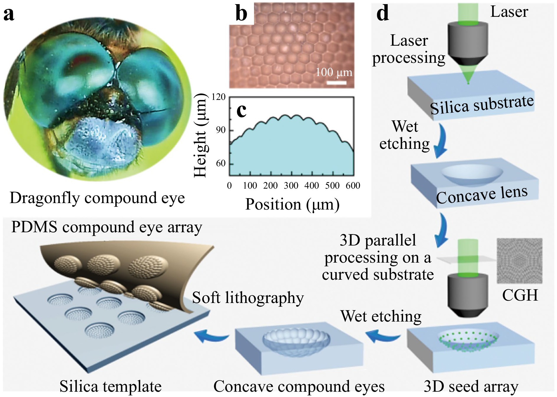
Fig. 1 The basic concept of the parallel fabrication of complex 3D compound eyes by fs-laser ablation and wet etching. a The compound eyes of a dragonfly. b Microscopic image of the insect compound eye. c The profile of the dragonfly compound eye. d Schematic illustration of the fabrication of 3D artificial compound μ-eyes.
The schematic illustration of the fabrication procedure is shown in Fig. 1d. During fabrication of the first concave surface, an un-modulated (single beam) fs-laser pulse was focused on the sample through an objective, inducing seed damage providing the pulse energy exceeds the ablation threshold. Subsequently, the seed damage gradually evolved into a spherical profile surface during wet etching. Seed damage can be created at a pre-designed depth that defines the lens curvature during the evolution of etching, and the aperture can be controlled well by the etching time. The 3D profile was measured with a laser confocal microscope (LSCM). To generate a 3D distributed focal spot array, we designed a Computer-Generated Hologram (CGH) using an Optimal Rotation Angle (ORA) method31 in which the focal spot array was focused on a curved surface simultaneously for holographic ablation (a parallel 3D surface processing). Thus, a 3D distributed seeds array was created for subsequent wet etching. Subsequently, the laser-induced seeds at different spatial positions were evolving into microlenses and overlapped with each other, forming a closely packed and curved MCLA (inverse compound eyes). By using this inverse compound eye as a hard template, artificial compound eyes of high quality and uniformity were mass-produced via a soft lithography process. This approach combines holographic ablation and wet etching and permits the direct fabrication of complex MCLA in a simple but highly efficient manner. method, revealing the great potential for parallel fabrication of microscale optical devices.
-
We first investigated the formation process of the large-size single concave lens designed as the main lens for the compound eye. Fig. 2a shows a schematic of the wet-etching-induced evolution from a laser-ablated seed into a single concave lens. For fabrication, an unmodulated femtosecond laser pulse was focused onto the surface of the silica with a pulse energy of 3.93 μJ (peak power density: 3.81×10¹⁵ W/cm2,32), inducing an initial seed with a size of approximately 3 μm, as shown in Fig. 2b. The ablation region underwent complex modification including melting, resolidification, and vaporization33. Subsequently, the sample was immersed in a 40% HF solution for 30 min. The seed evolved into a pit with a width of 13.8 μm and a depth of 12.5 μm owing to the faster (anisotropic) etching rate of the modified region34−36.
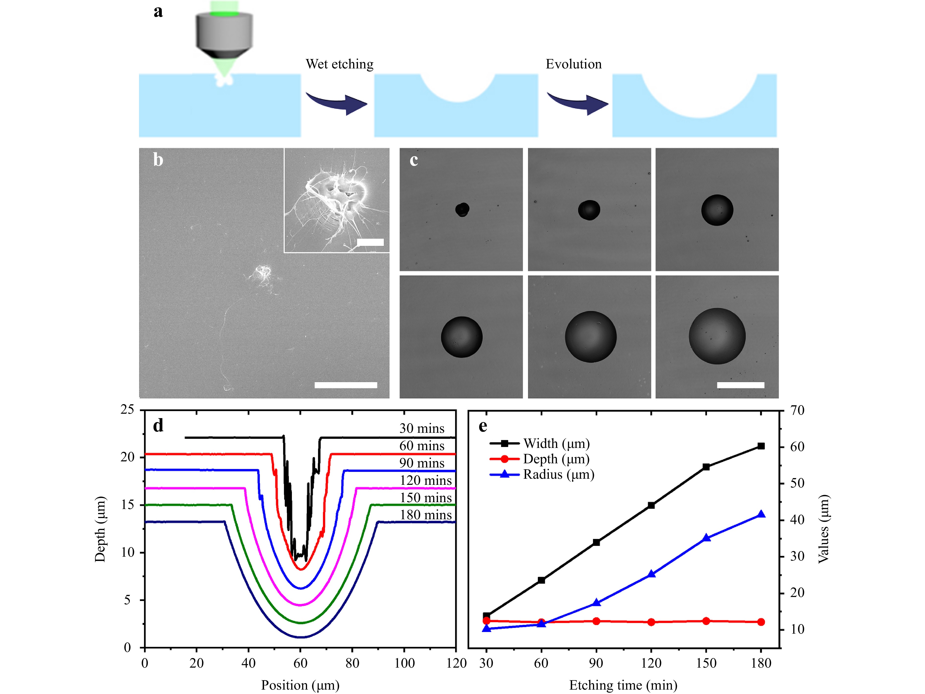
Fig. 2 a Schematic illustration of the evolution process from a laser-ablated seed to a single concave lens. b SEM image of an initial seed induced by a single fs-laser pulse with pulse energy of 3.93 μJ. c Top view of the structure after being etched for 30, 60, 90, 120, 150, and 180 min, respectively. d The cross-section profile of the structure under different etching times. e The values changes of the concave lens with etching time. Scale bar: b 20 μm, (inset) 2 μm, c 50 μm.
In addition, the proposed fabrication strategy is not limited to simple microlenses; it also enables the prototyping of 3D compound eyes. Using the ORA method, a CGH can be generated according to the designed 3D spot array shown in Fig. 3a. When a beam is modulated using the CGH, the corresponding 3D spot array is regenerated. A schematic is shown in Fig. 3b, which indicates the 3D distribution of the spot array. To confirm the 3D distribution, we experimentally measured the focal spots at different positions on a curved substrate. Fig. 3c shows the regeneration of spot arrays at different positions. At different propagation locations, different spot arrays (spot circles) were clearly identified, indicating a 3D distribution. By the way, the high-intensity peak in the center is the far off-focus of the $ 0^{th} $-order beam, which is blocked in the parallel writing.
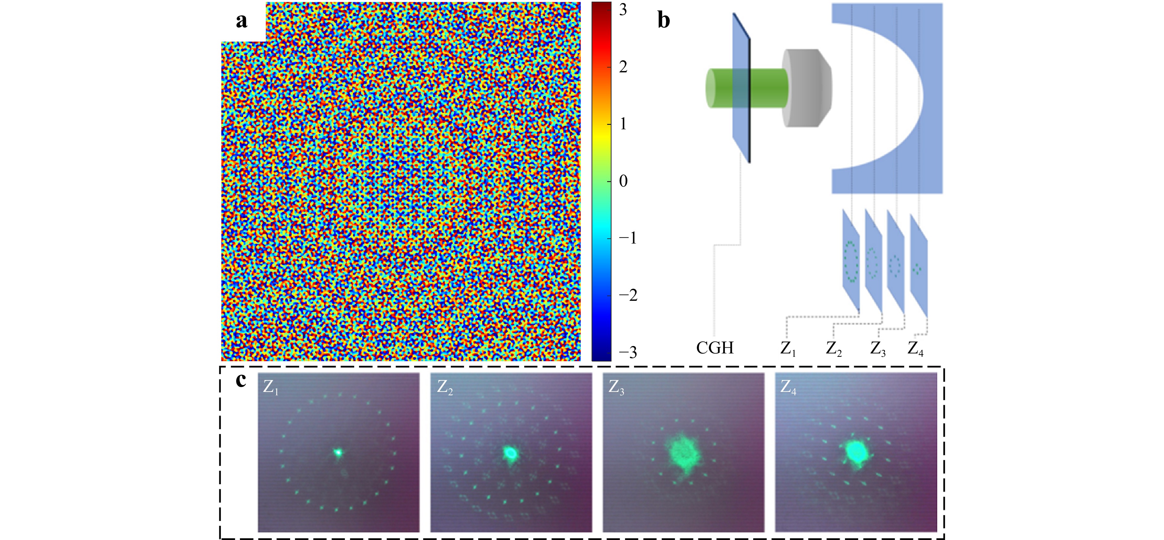
Fig. 3 a CGH generated using the ORA method according to a 3D spot-array. b Schematic of the regeneration of a 3D spot-array through CGH and an objective. c The light distribution at different propagation locations. The central intensity maximum is blocked in the laser ablation step.
For the fabrication of 3D compound eyes, a curved substrate after etching for 30 min is used for 3D exposure. The 3D profile was confirmed by LSCM, as shown in Fig. 4a. To align the 3D spot array with the curved profile, the $ 0^{th} $-order beam in the blue circle was used as the center to coincide with the center of the substrate border (red circle). The cross-profile of the 3D spot array produced by the second laser ablation is shown in Fig. 4b. Notably, the surface was very smooth with a roughness of less than 10 nm (measured using LSCM). The pattern of the 3D focal point array, defining the positions of 61 lenslets on a spherically curved surface, had a 10 μm spacing between them. The corresponding CGH shown in Fig. 3a was used for laser fabrication. The intensity distribution of the CGH was simulated using VirtualLab Fusion Software (LightTrans International UG). Fig. 4c shows the intensity distribution in the X-Z plane. Each focal spot had the same intensity and was located on acurved surface. Subsequently, the CGH was loaded into the SLM to expose the samples. In our study, a beam with a pulse energy of 11.3 μJ was divided into 61 beams through the SLM, and a 3D spot array was formed at the focal plane of the objective lens. The pulse energy at each spot was approximately 185 nJ, which equals a laser fluence of 29.3 J/cm2. Each spot is focused on a spherical surface profile. A 50-pulse exposure was used for the ablation of a 3D seed array, revealing the 3D parallel fabrication capability. Cross-sectional profiles of the spherical surfaces with pre-programmed ablation pits (seeds for wet etching) are shown in Fig. 4d. Each pit, having a similar size of about 1 μm, was located exactly on the 3D spherical surface. This proves that the size of the ablation region was independent of the spatial location of the focal spot, and that all foci were on the surface.
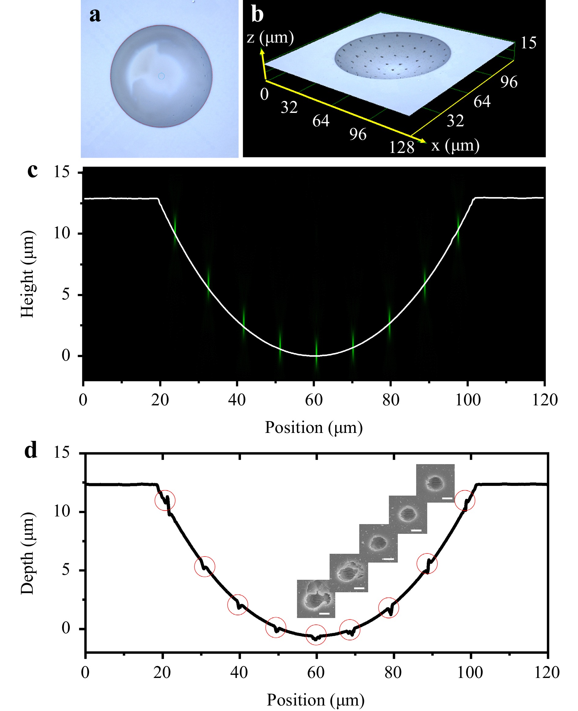
Fig. 4 a Top view of the curved substrate with 3D spot array located in the red circular region that is aligned with the center of the $ 0^{th} $-order laser beam in the blue circle). b Cross-section profile of the spherical surface with ablation pits. c The intensity distribution in the X-Z plane with VirtualLab Fusion Software of CGH in Fig. 3a. The white line is the cross-section line. d The cross-section profile of the distribution of laser-induced seeds on the surface of the concave lens. The insets are SEM images of the seeds at different depths. The scale bar is 1 μm.
To convert this 3D seed array into compound μ-eyes, the abovementioned sample was immersed in a 20% of HF solution for etching. The seeds evolved into a 3D ommatidium array within 40 min. The 3D profile of the as-obtained compound, μ-eye, was measured using LSCM (Fig. 5). The distance between each ommatidium is 10 μm. The location shift in the Z position between the outside and center of the lenslets was approximately 10 μm (on a curved surface). All ommatidia were closely packed (100% fill factor) on a spherical surface with a radius of approximately 100 μm. Furthermore, the radius of each ommatidium-lenslet on the cross-section was very uniform. Hence, their focal lengths are constant, which ensures a high focusing performance.
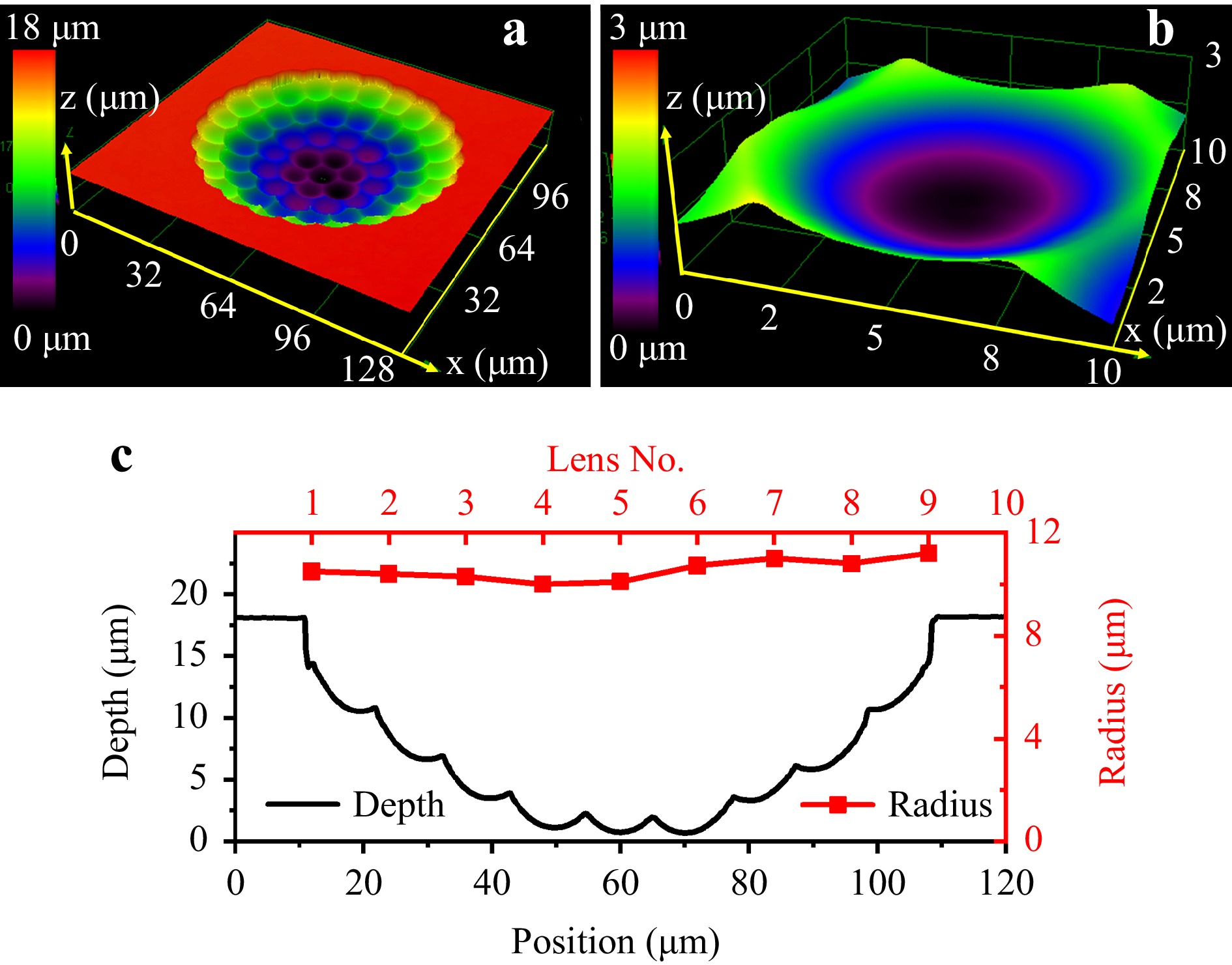
Fig. 5 a The 3D profilometer view of the lens array; b the 3D image of the central lenslet; c the average size and the cross-section profile of the compound eye.
-
The imaging capabilities of the 3D compound eye were investigated using an optical microscope. As shown in Fig. 6, for the compound eye, four images were obtained by adjusting the distance between the sample and objective. The imaging performance of the separate lenslets was well separated along the axial direction because of their different depth locations. The lenslets demonstrated excellent image quality, highlighting significant potential of 3D compound eyes in microimaging, optical communication, and integrated optics, particularly in scenarios where image acquisition without the use of moving parts is desirable.
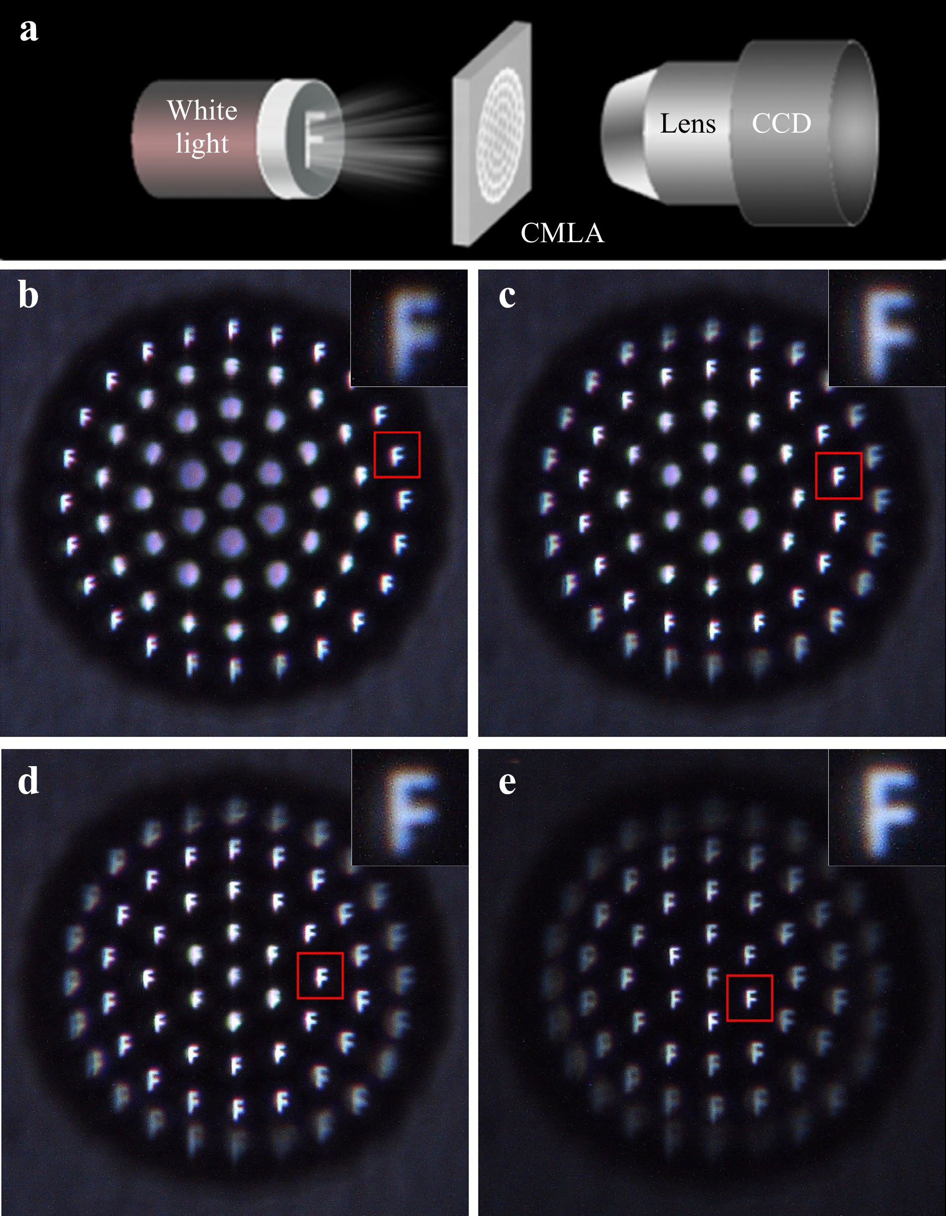
Fig. 6 a Schematic illustration of the setup for imaging test. b−e Optical images of letter F at different ommatidia (lenslets) of the compound eye.
-
The holographic laser fabrication of complex silica optical devices is scalable, and combination of laser holographic ablation and wet etching processes has significantly improved fabrication efficiency. However, practical production of such optical devices is still challenging due to the complexity and time consuming nature of the process. To address this issue, we demonstrate the mass production of soft micro-optical components using silica structures as hard templates. Soft lithography, a cost-effective and highly efficient technology, is employed to create inverse structures based on these templates. In this study, polydimethylsiloxane (PDMS) is utilized to fabricate soft optics. As depicted in Fig. 7, a PDMS μ-compound eye array was successfully fabricated using the corresponding silica templates. Scanning electron microscopy (SEM) images of these PDMS μ-compound eyes confirmed their high surface quality.
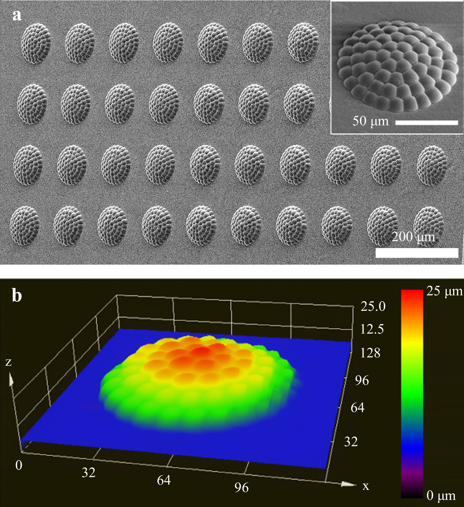
Fig. 7 a SEM images of PDMS μ-compound eye array fabricated through soft lithography technology using the silica μ-compound eyes as a template. The inset is a magnified SEM image of the compound eye. b 3D profilometer view of the PDMS μ-compound eye.
The curved profile enables the compound eyes to have a large field of view, but meanwhile, limits their focus position only positioned on a curved focal plane. For real bio-compound eyes, there is a fiber to receive light and to guide it right to the retina. However, it is difficult to make this compatible with the current procedure, in sensors and it is difficult to integrate optics and detectors on chip. In theory, the parameters of each lenslet, including its height, curvature, and focal length, should be redesigned. Thus, their focus was on a flat plane according to its position on the curved profile. Clearly, this is a formidable and difficult task. Therefore, we propose a deep-learning algorithm based on generative adversarial networks (GAN) for image processing. In this study, two neural networks were utilized to maximize the generative power of the discriminator and minimize its loss function, whereas the discriminator was trained to maximize its loss function (Fig. 8a). The generator in GAN takes the source images $ I_{a} $ and $ I_{b} $ as input, aiming to generate the focus map F. The goal of the generator is to reconstruct the focus maps as accurately as possible, whereas the purpose of the discriminator is to distinguish the generated focus maps from the real ones. G includes an encoder, a tensor concatenation module, and a decoder. The network in the encoder and decoder is comprised of Convolutional Neural Network (CNN). In the encoder, the source images are mapped as features using a CNN. In the decoder, the joint feature is deconvolved using two convolutional layers for size recovery and reconstruction. In the tensor concatenation part, the features extracted by the encoder were concatenated. The loss function plays a crucial role in deep learning for optimizing the network parameters. The loss functions are expressed by Eqs. 1, 3: We trained D to maximize the probability of assigning the correct label to both the training examples and the samples from G. We train G to simultaneously minimize $ \log(1 - D(G(I))) $ at the same time. D and G are optimized to achieve the Nash Equilibrium with the loss function $ L(G,D) $:
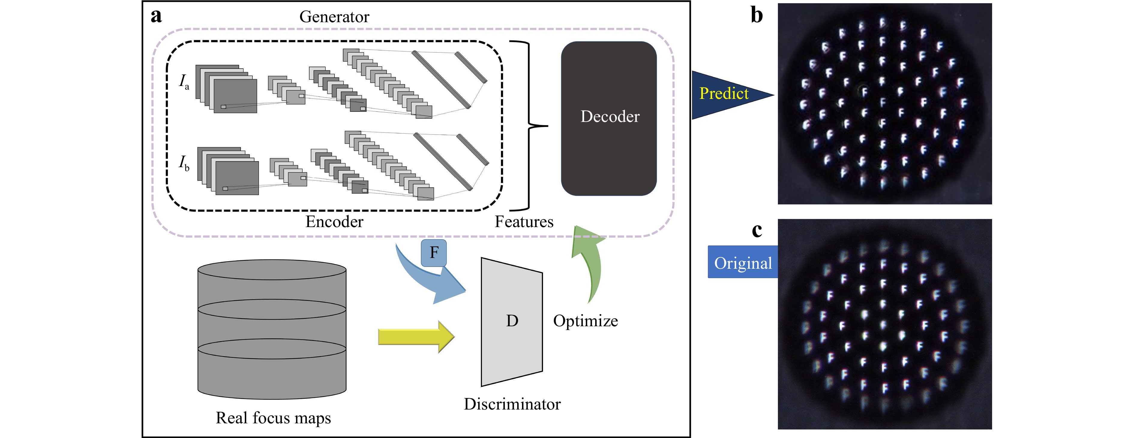
Fig. 8 Image restoration using the generative adversarial network (GAN). a Schematic illustration of the GAN. b The predicted image using GAN with the original image in c.
$$ \begin{aligned} L(D, G)=&\mathbb{E}_{x-p_{\text {data }}(x)}[\log D(x)]\\&+\mathbb{E}_{I-p_{I}(I)}[\log (1-D(G(I)))]\\=&\int_{x} p_{\text {data }}(x) \log (D(x)) d x \\&+\int_{I} p_{I}(I) \log (1-D(G(I))) d I \end{aligned} $$ (1) Where $ p_{\rm{data}} $ is the generator’s distribution over real focus data x, and pI is source image distribution. We represent a mapping to data space as $ G\left(I_{a} ; I_{b} ; \theta_{g}\right) $, where $ \theta_{g} $ is the trainable parameters of G. Additionally, we define a second network $ D\left(F ; x ; \theta_{d}\right) $, which outputs a single scalar.
By assuming that $ x = G(I) $ is reversible in variable substitution, where pG is the generated distribution, we get the following equation:
$$ \begin{aligned} L(D, G)=&\mathbb{E}_{x-p_{\text {data }}(x)}[\log D(x)]\\&+\mathbb{E}_{x-p_{G}(x)}[\log (1-D(x))] \end{aligned} $$ (2) the above process can be expressed as followed,which is equivalent to Jensen–Shannon divergence.
$$ \begin{aligned} \min _{G} \max _{D} L(D, G)=&\mathbb{E}_{x \sim p_{\text {data }}(x)}[\log D(x)]\\&+\mathbb{E}_{x \sim p_{G}(x)}[\log (1-D(x))] \end{aligned} $$ (3) Uniform and clear images were obtained after simulations. As shown in Fig. 8a, the neural network was trained to achieve image restoration for all the eyes using the images shown in Fig. 8c. Image restoration does not depend on the incident wavelength, material refractive index, or single-lens thickness. With this technology, compound eye imaging retains a large field of view and significantly improves the image quality, making it available for a wider range of application scenarios (Fig. 8b).
-
In summary, we introduced a method for 3D parallel fabrication assisted by wet etching to fabricate 3D MCLA on curved surfaces. The relationship between the surface ablation conditions and the etching time was analyzed. The etching rate of silica in the HF solution (40%) was $ 0.25\pm 0.03$ μm/min. A spherical surface with a radius of 74 μm and roughness smaller than 10 nm was fabricated after single-focus ablation. The width and depth of the lens were 84.1 μm and 12.8 μm, respectively. A 3D MCLA on the spherical surface with a radius of 100 μm was fabricated. Each lens has the same radius of 10 μm, indicating that the focal length is independent of the spatial location. Using a generative adversarial network (GAN), image restoration was conducted for each eyelid on a curved profile. Above all, this work provides a technology for the 3D parallel processing of complex micro-optical devices, such as compound eyes.
-
Setup: In our experiments, a 3D holographic fs-laser parallel processing system was built, which contained an fs-laser amplifier system (Pharos PH1-SP-1mJ, Light Conversion Ltd.), a phase-only Liquid Crystal-On-Silicon Spatial Light Modulator (LCOS-SLM, LETO, HOLOEYE Photonics AG), an XYZ stage, and an objective lens with a numerical aperture (NA) of 0.7. The center laser wavelength, pulse duration, maximum repetition rate, and maximum pulse energy were 1030 nm, 190 fs, 200 kHz, and 1 mJ, respectively. The XY stage was a motorized linear stage powered by a step motor with a resolution of 100 nm and a maximum stroke of 20 mm. The LCOS-SLM’s pixel pitch was 6.4 μm, and the resolution was $ 1920\times 1080 $. The Z stage is a piezo stage with a resolution of 1 nm and a maximum stroke of 100 μm.
Samples: The sample used in the experiment is fused silica (JGS1) with a thickness of 300 μm, which was bought from GoldDragon Optics Electronic Technology CO., Ltd. The samples were cleaned with acetone, alcohol, and deionized water before laser irradiation.
Laser processing: The laser beam irradiated on the SLM through a nonlinear-optical beta-barium borate (BBO) frequency-doubling crystal and a beam expander ($ M = 3 $) consisting of a pair of lenses with focal lengths of -50 mm and 150 mm, respectively. Consequently, the actual center wavelength of the fs-laser for fabrication was 514 nm. Subsequently, the modulated beam was transferred to the entrance of the objective through a 4-F optical system consisting of two plano-convex lenses with focal lengths of 400 mm and 300 mm. Finally, the modulated beam is converted into a designed 3D spot array via the Fourier transform (FT) using an objective lens. During this process, an optimal rotation angle (ORA) method was used to split the beam into 61 spots. The coordinates of the focal points on the 3D profile were first obtained and then used for hologram calculations according to the ORA method. These 3D spot arrays were then used for parallel ablation. To avoid the $ 0^{th} $-order beam, a hologram of the blazed grating was added to generate the $ 1^{st} $-order and $ 0^{th} $-order beams, in which the former (with an efficiency of 25%) was used for fabrication while the latter was blocked. All pulse energies were measured after SLM. The objective lens transmittance was approximately 96%.
Wet etching: All three types of irradiated samples were immersed in an HF solution and etched with ultrasonic treatment at room temperature. For single-spot laser irradiation, the concentration of the HF solution used was 40%, and for the other solutions, it was 20%. Each type of structure had a different etching time, which could influence the final surface profile. After etching, the sample was cleaned with deionized water, and micro-optics were formed.
Surface and imaging characterization: The surface of the fabricated micro-optics was measured using a laser confocal microscope (LSCM, LEXT OLS4100, Olympus). The optical performance of the microoptics was characterized using a commercial optical microscope. The light was patterned by a hollow letter “F”, which acted as the object. The images were magnified using an optical microscope and captured using a charge-coupled device (CCD).
Production of PDMS micro-optics through soft lithography: The PDMS prepolymer was mixed with a crosslinker (mass ratio of 10:1) and is centrifuged for 5 min at a speed of 3000 rotations/min to remove the gas. The PDMS prepolymer was then dropped onto a silica template and cured at 95 °C for 1 h. Subsequently, the PDMS micro-optics were cured and peeled from the template. The surface profile of the PDMS micro-optics was measured using scanning electron microscopy (SEM; JEOL JSM-6700F) and LSCM.
-
National Key R&D Program of China (2021YFB2802000); National Natural Science Foundation of China (61827826, 62175086, 62131018); Natural Science Foundation of Jilin Province (20220101107JC); Education Department of Jilin Province (JJKH20221003KJ); Interdisciplinary Integration and Innovation Project of JLU (JLUXKJC2021ZZ15); All authors thank Prof. Yong-Lai Zhang for the valuable discussions and draft writing advice. All authors thank Mr Shi-Lei Wang and Mr Zheng Dong for the capture of dragonfly eyes.

 DownLoad: