


-
With the rapid advancements in communication and computing technologies, there is a growing demand for real-time reconfigurable optical elements. Among the extensively studied reconfigurable optical devices, microlens arrays are key elements that show promise in various applications, such as autostereoscopic display1, 2 , autofocusing optical lens3, AR/VR displays4, optical communication5, integral imaging6−13, etc. For example, microlens arrays are the critical components in integral imaging, which were used to collect and display images. Among various 3D displays configurations, integral imaging is one of the most attractive technologies due to its ability for providing continuous viewpoints and full parallax images. However, in integral imaging, the 3D images can only be clearly reconstructed at the central depth plane (CDP), limited by the fixed focal length of the microlens arrays6−9 used. To overcome this limitation, adjustable microlens arrays have been proposed for 3D display applications10−13. These tunable microlens arrays allow for adjusting the position of the CDP, thereby exploring greater image depth.
Thus far, various approaches have been demonstrated to construct reconfigurable/tunable microlenses, such as adaptive liquid microlenses14−18, adaptive metalenses19−26, strain responsive microlenses27, 28, photoswitchable microlenses29, thermal responsive microlenses30. Liquid crystal (LC) with electrically31−36, optically37, 38, or acoustically39, 40 tunable refraction has been exploited extensively for tunable microlens arrays41−51. The reported approaches to construct LC tunable microlens arrays can be divided into two major types: (i) a combination of a passive solid-state lens array and an LC modulator, and (ii) a gradient refractive-index profile of an LC layer generated with an axially symmetric electric field based on specially designed electrode patterns. Both construction approaches involve multiple fabrication processes, increasing fabrication complexity and cost.
Here, we demonstrate an electrically tunable LC microlens array using a simple, single-step fabrication method based on photopolymerization-induced phase separation (PIPS) inside a polymer/LC composite52. This results in phase-separated composite films (PSCOFs)53 containing adjacent layers of LC and polymer. The LC microlens array exhibits high focusing and imaging quality with polarization-dependent, electrically tunable focusing properties. This unique fabrication technology stands in contrast to reported methods such as inkjet printing54, compression molding55, thermal reflow of photoresist56, and three-dimensional printing57, offering a facile, single-step, low-cost, and high-throughput production process. Finally, we demonstrate the practical applications of this microlens array by achieving image acquisition and electrically tunable CDP in 3D displays.
-
Fig. 1a, b illustrate the schematic of the UV exposure and phase separation processes, respectively. As previously reported52, when a cell filled with a mixture of LC and prepolymer is exposed to a normally incident, collimated UV laser beam, an intensity gradient of the UV exposure beam is created along the z-direction inside the cell due to the strong absorption of UV light. This intensity gradient leads to a complete phase separation along the z-direction. By using a suitable photomask (Fig. 1c) during UV exposure, an additional intensity gradient is created in the x-y plane of the cell, as shown in Fig. 1d. The NOA65 monomers in the high-intensity regions near the UV beam undergo polymerization first, while those in the low-intensity regions diffuse towards the high-intensity regions to maintain their relative concentration, causing the LCs to be expelled from the polymerization regions inside the cell. With precise exposure conditions, extended UV exposure completely consumes all the NOA65 monomers and drives the LCs out of the polymerized volume. At the same time, the LC molecules align with the alignment layer. Consequently, the phase separation is anisotropic in three-dimensional space inside the cell. Depending on the patterns of the photomask, complex microstructures of pure LCs with various shapes and sizes can be fabricated. Using a grayscale photomask (Fig. 1c), a 3D phase separation occurs to form a microlens array inside the LC cell. The entire phase separation process for microlens array formation is also depicted in a cartoon movie (see the supplementary video S1).

Fig. 1 a Schematic of the UV exposure and b phase separation processes. c Designed grayscale photomask. Inset shows a single pattern with gradient transmittance (gradually increase from center to edge). d Generated 3D light intensity distribution from the photomask. Each pattern has a diameter of 200 μm and the pattern period is 240 μm.
During the fabrication process, the curing temperature and UV intensity are crucial factors significantly influencing the phase separation of the polymer and LCs, as well as the alignment of the LC molecules. Temperature has a major effect on the bulk viscosity of the E7/NOA65 mixture, but it has little influence on the polymerization rate. Instead, the polymerization rate is highly dependent on the UV intensity, with the bulk viscosity reducing greatly as the temperature increases58. At low curing temperatures, the diffusion rates of both LCs and monomers are low due to high viscosity, resulting in incomplete phase separation and the formation of PDLC-like structures. This, in turn, deteriorates the alignment of the LC molecules and causes non-negligible scattering. On the other hand, high UV intensity during monomer polymerization leads to fast polymerization, which can prevent LC molecules from diffusing out of the polymerization region, resulting in a rough polymer surface and subsequent scattering. To strike a balance between the performance of the LC microlens and the curing time, a relatively low UV intensity is desired. Therefore, during our experiments, we maintained a high temperature (~100 °C) and a low UV intensity (1.25 mW/cm2) to achieve complete phase separation and a smooth LC-polymer interface.
-
The textures and morphologies of the fabricated microlens array were first investigated. To study the effect of the LC cell gap on the focal length and other properties of the microlens, we prepared samples with cell gaps of 10, 15, and 20 μm, respectively. Fig. 2 shows the observed textures of the cell after UV exposure under a polarizing optical microscope (POM). When the polarization direction of either polarizer is parallel to the alignment direction, the cell demonstrates a completely dark state (Fig. 2a1, 2a3). However, when the polarization direction has a 45° angle with respect to the alignment direction, we can clearly see that periodically patterned structures are formed inside the cell, as shown in Fig. 2a2. The observed colors, called interference colors, result from the optical interference of the o-ray and e-ray59. The interference colors are determined by the birefringence Δn and the thickness of the LC layer. Because the birefringence is constant, the interference colors are only related to the thickness of the LC layer. Therefore, we can evaluate the structure inside the LC cell through the interference color. In each single pattern, a set of concentric fringes is clearly visible in the regions with the fringe color changing from red to blue from the center to the edge, indicating a continuous variation of the optical path length. Similar results are observed in Fig. 2b, c for cell gaps of 15 and 20 μm, respectively. As the cell gap increases, the number of concentric fringes gradually increases, and the colors become more abundant, indicating an increasing thickness between the center and the edge of the LC layer in every single pattern. Notably, there is a dark line in the middle of each microlens in Fig. 2c1, c3. The dark line is called the disclination line, which is common in LC lenses60. The major reason of the disclination line comes from the interaction between the anchoring of the top curved surface and the bottom alignment layer. The curved surface of the polymer layer provides a non-uniformly axially-symmetrical alignment of the LC molecules, hence causing a disclination line. Increasing the pretilt angle or applying an extra in-plane electric field is an efficient way to suppress the disclination line60, 61.

Fig. 2 Characterization of the fabricated LC cell and polymer layer. POM images of the cell when the alignment direction was a1 0°, a2 45°, and a3 90° with respect to the polarization direction of the polarizer when the cell gap is 10 μm. Scale bar: 500 μm. a4 The 2D surface profile of the polymer layer. The color bar indicates the height of the film. a5 The sag height distribution of the film along the white dash line in a4. b, c Corresponding results for the cases with the cell gaps of 15 and 20 μm, respectively. d The photograph of a typical large-area sample under crossed polarizers. e The AFM image of the polymer layer. f The height distribution of the film along the white dash line in e.
To confirm our observations, the surface morphologies of the polymerized NOA65 were investigated using a scanning white light interferometer. Fig. 2a4, b4, c4 show the 2D profile images, clearly demonstrating the periodic bowl-like polymeric microstructures. The cross-sectional profiles of the microlens arrays (Fig. 2a5, b5, c5) show the height distributions. The average sag heights of the microlens arrays are 2.75, 4.13, and 7.24 μm in the three different cells, with each microlens having a diameter of about 200 μm. As expected, the sag height of the microlens increases with the increase of the cell gap. To demonstrate the large-area fabrication capability of our proposed technique, we prepared a sample with an effective working area of 5 × 5 cm2, as shown in Fig. 2d, which consists of 44100 microlenses in total. In Fig. 2d, a colored ring can be clearly observed for the large-area sample that is mainly caused by the uneven cell gap. When preparing the LC cell, the spacers were only distributed on both sides of the LC cell. The cell gap gradually decreases from the edge to the center due to the gravity effect. Therefore, the interference-induced colors of the large-area sample also gradually changed from the center to the edge. Fig. 2e shows the result of the atomic force microscope (AFM) of the polymer layer at the center of the microlens, which has a relatively smooth surface. Fig. 2f shows the height of the cross-section labeled by the white dashed line in Fig. 2e. The calculated root mean square (RMS) is 1.963 nm, which further indicates that the prepared microlens has high-quality surface smoothness compared with other reported methods54−57. Moreover, the microlens arrays we fabricated have a high transmittance of ~70% in the whole visible range of 400-800 nm, as shown in Figure S1 in the supplementary information, indicating their high-quality performance and suitability for various applications.
We further compared the formed surface profiles of the microlens array with the designed mask. Fig. 3 shows the gray distribution of the designed mask (green line), the light intensity distribution generated by the mask (red line), and the microlens profile (blue line) along the microlens center, respectively. Evidently, the formed surface profiles of the microlens array closely match the light intensity distribution generated by the designed mask, indicating the high fidelity of the photopolymerization-induced phase separation.

Fig. 3 The gray distribution of the designed mask (green line), the light intensity distribution generated by the mask (red line), and the microlens profile (blue line) along the microlen’s center.
As designed, the LC molecules should ideally have a preferred orientation following the preset direction by the alignment layer. Therefore, the focusing spots of such a microlens array should be both polarization-dependent and electrically tunable. We employ two approaches to adjust the focusing properties of this microlens array. The first approach involves changing the polarization direction of incident light. In our configuration, if the polarization direction of the incident light is parallel to the alignment direction of the LC molecules, the effective index of LCs experienced by the incident light is close to ne. Since ne > np, the microlens array works as a planar-convex microlens array, exhibiting a positive focal length. On the other hand, if the polarization direction of the incident light is perpendicular to the LCs’ alignment, the incident light will see the effective index of LCs close to no. In this case, no ≈ np, the microlens array becomes an optically homogeneous plate without any focusing properties. For simplicity, we characterized the focusing properties of the microlens array with a cell gap of 10 μm. The experimental results (Fig. 4a1−a4) demonstrate CCD-captured optical images at the real focal plane of the microlens array with different polarization directions of the incident light (see the supplementary video S2). Fig. 4b1−b4 show the sharp point spread function of the focus spots, confirming that the microlens array has excellent focusing points at θ = 0° (i.e., the polarization direction of the incident light was parallel to the alignment direction of LC molecules). As the polarizer rotates from 0° to 90°, the focusing intensity of the incident light gradually decreases. The focusing points disappear entirely when θ = 90° (i.e., the polarization direction of the incident light was perpendicular to the alignment direction of LC molecules). This experimental observation validates our hypothesis, indicating that the LC molecules have been aligned very well by the alignment layer.

Fig. 4 Focusing properties of the microlens array. a 2D and b 3D intensity distribution at the focal plane that can be tuned by polarization direction of incident light; c 2D and d 3D intensity distribution at the focal plane under different applied voltages; e Normalized intensity change as a function of the applied voltage at the fixed focal plane; f Measured focal length as a function of the applied voltage. Scale bar: 500 μm.
The other approach to tuning the microlens array involves applying an external electric field. The CCD-captured optical images at the focal plane of the microlens array with different applied voltages when the polarization direction of the incident light was parallel to the LC molecules’ alignment direction are shown in Fig. 4c1−c4 (see the supplementary video S3). Fig. 4d1−d4 demonstrate the corresponding point spread function of the focus spots at different applied voltages. By fixing the CCD at the initial focal plane, it can be observed that the focusing points become gradually defocused as the applied voltage increases. Understandably, with an increase in the applied voltage, the LC molecules realign along the direction of the external electric field. By applying a sufficient voltage, the LC molecules will be completely realigned along the direction of the external electric field, resulting in the condition that the incident light will only experience the ordinary refractive index, no, of the LCs regardless of the polarization directions. Again, in this case, no ≈ np, and the microlens array becomes an optically homogeneous plate without any focusing properties. This can be confirmed from the observation of the microlens array by rotating the polarizer from 0° to 90° at the applied voltage of 5 V (see the supplementary video S4). It shows a completely dark state regardless of the polarization of the incident light, indicating that the LC molecules are fully aligned along the electric field direction. Fig. 4e further characterizes the focusing properties of the microlens array in more detail. It is observed that at an applied voltage of 5 V, the microlens array has almost no focusing effect. Fig. 4f shows the experimentally measured dependence of the focal length on the applied voltage. We can see that the initial focal length of the microlens array is about 8 mm at V = 0 V. At the applied voltage of V = 2.8 V, the incident light beam starts to defocus at the initial position and focus at a longer distance. As the applied voltage increases, the focal length of the microlens becomes large. At V = 5 V, the focal length of the microlens is 20 mm.
The focal length f of each microlens can also be calculated using the formula $f = {{{R^2}} \mathord{\left/ {\vphantom {{{R^2}} {2d\left( {{n_{{\text{LC}}}} - {n_{\text{p}}}} \right)}}} \right. } {2d\left( {{n_{{\text{LC}}}} - {n_{\text{p}}}} \right)}}$ (Ref. 48), where R is the radius of the microlens’s surface, d is the sag height of the microlens surface, nLC is the effective refractive index of LCs, and np is the refractive index of the polymer. The nLC can be effectively tuned by applying an external electric field, allowing for convenient focal length adjustment of the microlens. For the aligned state, the effective value of nLC is polarization-dependent for the impinging light. When the polarization is parallel to the LC director, the light beam sees the extraordinary refractive index (i.e., nLC = ne = 1.746) of LC E7, while the polymer used is NOA65 with the refractive index of np = 1.524. At V = 0, the calculated focal length is 8.19 mm, which is in good agreement with the experimental result.
To evaluate the imaging quality of the microlens array, a hand-written capital letter “F” on a piece of glass was used as an object, and the microlens array was set in front of it. A CCD camera was positioned right behind the sample. Series of images were captured at different positions, as shown in Fig. 5a1−a4 (see the supplementary video S5). Fig. 5a1 shows the imaging of the microlens array at the focal plane, showing no clear imaging quality. This focal plane was set as the neutral position of z = 0. As the CCD moved away from the microlens array, a clear image of the handwritten letter was observed, with the size of the image gradually magnifying as the distance z increased, as shown in Fig. 5a2−a4. Once again, the imaging properties of our microlens array are both polarization-dependent and electrically tunable. Fig. 5b1−b4, c1−c4 show the imaging quality of the handwritten letter “F” under different polarizations of the incident light (see the supplementary video S6) and applied voltages (see the supplementary video S7), respectively, when the CCD’s position is fixed at z = 6.3 mm.

Fig. 5 The imaging properties of the microlens array. a The images at different imaging plane by changing CCD’s position; The images under b different polarizations of incident light and c different applied voltages. Scale bar: 250 μm.
The point spread function (PSF) of the microlens arrays was measured using a simple optical setup. A semiconductor laser with a working wavelength of λ0 = 532 nm was employed, and its laser beam was expanded and collimated using a spatial filter and a convex lens. The beam then passed through a polarizer with the polarization direction parallel to the rubbing direction of the sample. A 5x objective with a numerical aperture (NA) of 0.13 was used to capture the focal spots of the microlens array on the CCD.
For a diffraction-limited lens, the intensity distribution of the focal spot in the image plane is equivalent to the circular aperture-induced Airy pattern due to Fraunhofer diffraction. Given that a high-quality objective can be considered as a diffraction-limited lens, we can calculate the PSF of the lenses using the following formula, where J1 is the first-order Bessel function, $ k = {{\pi \cdot NA} \mathord{\left/ {\vphantom {{\pi \cdot NA} \lambda }} \right. } \lambda } $ and NA is the numerical aperture:
$$ g\left( r \right) = {{{J_1}\left( {kr} \right)} \mathord{\left/ {\vphantom {{{J_1}\left( {kr} \right)} {kr}}} \right. } {kr}} $$ (1) If we assume that each microlens is also diffraction-limited, its amplitude PSF can be also written as,
$$ f\left( r \right) = {{{J_1}\left( {kr} \right)} \mathord{\left/ {\vphantom {{{J_1}\left( {kr} \right)} {kr}}} \right. } {kr}} $$ (2) In our experiments, with NA = 0.13 and λ0 = 532 nm, the diameter Dobj of the Airy disc can be obtained from Dobj = 1.22λ0/NA = 4.9926 μm. As the prepared circular microlens has a radius R = 100 μm and f = 8 mm, the diameter Dml of the Airy disc can be obtained from Dml = 1.22fλ0/R = 51.923 μm. As the focused image undergoes the microlens and the objective, the measured intensity profile should be the square of the convolution between the amplitude PSFs of the microlens and the objective, which can be expressed as$I\left( r \right) = {I_0}{\left[ {f * g} \right]^2}$ (Ref. 51). Thus, the light intensity captured by the CCD can be expressed as follows:
$$ I ( {x,y} ) = {I_0}{\left[ {\int {\int_{ - \infty }^{\infty} {f\left( {{r'}} \right)g\left( {r - {r'}} \right)dr} } } \right]^2} $$ (3) Fig. 6 shows the measured and calculated intensity distribution of the microlens focal spot. To determine the PSF of the prepared microlens, we used Eq. 3 to fit the experimental data (blue circle curve), as shown in Fig. 6a3, b3, c3. The results in Fig. 6 allow us to obtain the diameter D of the focal spot. The measured and calculated results of the microlens arrays with different cell gaps are shown in Table 1. It is evident that the experimental results align well with the theoretical curves, indicating that the fabricated microlenses are nearly diffraction-limited and of high quality.

Fig. 6 Measured and calculated intensity distributions of the focal spot of the microlens with the cell gaps of a 10, b 15, and c 20 μm, respectively. The intensity distributions of the focused spot at a1, b1, c1 the x-z plane and a2, b2, c2 the x-y plane. a3, b3, c3 The measured (blue circle curve) and calculated (red solid line) intensity distribution of the focal spot of the microlens.
Cell gap (μm)
Sag height d (μm)
Focal length f (mm)
Measured diameter Dexp (μm)
Calculated diameter Dcal (μm)
10
2.75
8
52.5
51.923
15
4.13
4
27.5
25.962
20
7.24
3
22.5
19.471Table 1. Measured and calculated results of the microlens with different cell gaps.
To further evaluate the imaging quality of the fabricated microlens array, a negative 1951USAF resolution chart (Thorlabs, USA) was used, which has 10 groups (−2 to +7) of patterns, each consisting of 6 elements. Fig. 7a presents the original patterns, while Fig. 7b, c show the imaged chart of element 3 and 4 of group 3, respectively. It can be observed from Fig. 7b that each microlens is capable of resolving beyond element 3 of group 3, indicating that the microlens resolution is better than 10.10 lp/mm. Another crucial parameter for the LC microlens arrays is the response time. Fig. 8 shows the measured rising and falling times of the microlens arrays with different cell gaps. The rising time refers to the realigning process of LC molecules from the initial state to a new stable state under an applied voltage, defined as the time when the transmitted intensity changes from 90% to 10%. The falling time refers to the self-relaxation process of LC molecules that return to the initial state after the removal of the applied voltage. The rising time and falling time for homogeneous LC cells can be calculated using the following equations62:

Fig. 7 Imaging quality evaluation of the PSCOF microlens array. a The original image of the negative 1951USAF resolution chart; b, c The imaged chart of element 3 and 4 of group 3, respectively.

Fig. 8 Measured response time of the PSCOF microlens arrays with the cell gaps of a 10, b 15, and c 20 μm, respectively. The cell gap, applied voltage and corresponding response time are shown in the top-left corner. d The response time versus the applied voltage ranging from 5 to 20 V for different cell gaps.
$$ {\tau _{rise}} = \frac{{{\gamma _1}{d^2}}}{{{K_{11}}{\pi ^2}\left| {{{\left( {{V \mathord{\left/ {\vphantom {V {{V_{th}}}}} \right. } {{V_{th}}}}} \right)}^2} - 1} \right|}} $$ (4) $$ {\tau _{fall}} = \frac{{{\gamma _1}{d^2}}}{{{K_{11}}{\pi ^2}}} $$ (5) where γ1 is the rotational viscosity, K11 is the elastic constant, V and Vth are driving and threshold voltages, respectively, and d is the cell gap. The results show that as the cell gap increases, the response time also increases, as expected. Fig. 8d illustrates the response time versus applied voltage for different cell gaps. It is evident that the response time decreases with the increased voltage. For samples with cell gaps of 10 μm and 15 μm, when the applied voltage is larger than 11 V, the response time does not decrease significantly, indicating that 11 V is the saturation voltage. For the sample with a cell gap of 20 μm, the saturation voltage is 16 V. It is worth noting that the rising time of the sample with a cell gap of 15 μm is larger than that with a cell gap of 20 μm. From Eq. 4, we can see that the rising time is highly dependent on the cell gap and the driving voltage. In our experiment, the driving voltage for the sample with a cell gap of 15 μm is higher than that with a cell gap of 20 μm, resulting in a shorter rising time.
-
Based on the superior properties of the prepared microlens array, we further applied it for the integral imaging application. Firstly, the elemental image array (EIA) was captured by the microscopy system that consists of an objective and a CCD. The photomask designed by the EIA serves as the background display panel. The detailed capturing progress is described in Supplementary Information. Then, a white light source was used to illuminate the photomask and imaged by the microlens array in front of the photomask. Based on the reversibility principle, the reconstructed objects “3” and “D” were produced at different positions in the air and then captured by the microscopy system. The optical setup is illustrated in Fig. 9a. To confirm the spatial position of the two reconstructed objects, we can move the position of the microscopy system to achieve a sharp and clear image. When the focal plane of the microscopy is on the object “3”, it can be clearly seen while the object “D” is blurred, as shown in Fig. 9b. When the focal plane is moved to the middle between the objects “3” and “D”, the sharpness of both is the same, as shown in Fig. 9c. When the focal plane is on the object “D”, we can see a clear “D” but a blurred “3”, as shown in Fig. 9d. Additionally, we provide a movie captured by the microscopy with continuously changed position along the optical axis (see the supplementary video S8). From the video, it is evident that the object “3” becomes blurry while the object “D” becomes clear gradually. One distinct advantage of the LC microlens array is that it has adjustable focal length, therefore we can conveniently change the CDP position by electrically tuning the focal length. The CDP location can be calculated by the following formula:
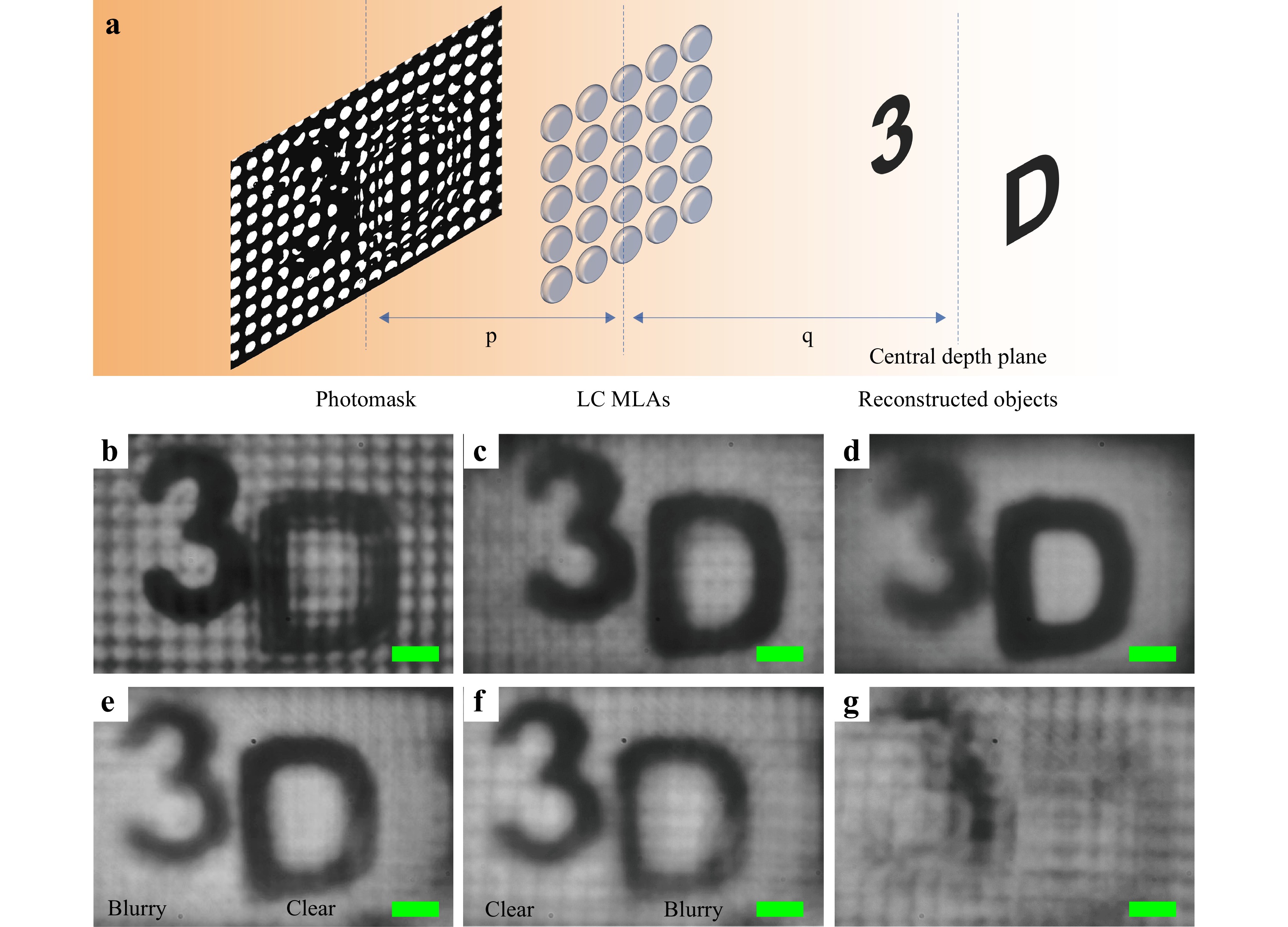
Fig. 9 Schematic of 3D image reproduction. a A white light source illuminated the photomask which was designed based on the EIA captured by the CCD; The image captured by the microscopy system at different positions: b on the object “3”; c in the middle between the two objects; d on the object “D”; The image captured by the microscopy system at different applied voltage on the microlens array: e V = 0 V; f V = 3.5 V; g V = 15 V. Scale bar: 500 µm.
$$ \frac{1}{f} = \frac{1}{p} + \frac{1}{q} $$ (6) where f is the focal length of the microlens, p is the distance between the photomask and the microlens array, while q is the distance between the microlens array and the CDP. First, the object “D” is clearer than the object “3” when there is no voltage applied, as shown in Fig. 9e. After applying 3.5 V on the microlens array, the object “3” is clearer than the object “D” because the focal length of the microlens array becomes larger and the CDP moves backward. At this moment, the microscopy’s focal plane is closer to the object “3”, as shown in Fig. 9f. When applying 15 V on the microlens array, the focal length of the microlens tends to be infinite. In such a case, the microlens array just becomes a transparent medium without focusing function. As a result, the integral imaging system displays in 2D mode and both the “3” and “D” images become blurry, as shown in Fig. 9g. Therefore, one can conveniently switch the display mode between 2D and 3D by electrically controlling the LC microlens array.
-
In summary, we have demonstrated an electrically tunable microlens array using the simple PSCOF approach. The LC microlens array demonstrates polarization-dependent, electrically tunable focusing properties. Without applied voltage, the microlens has a natural focal length of 8 mm due to its inherent gradient index profile. By adjusting the cell gap, the initial focal length can be controlled. Beyond a certain voltage threshold, LC reorientation occurs, and the focal length gradually increases. The near-diffraction-limited performance of the LC microlens array makes it a valuable component for integral imaging.
Furthermore, the fabrication process is simple and cost-effective, involving only a one-step exposure process. This feature, combined with the microlens array’s flat, ultra-thin design and excellent tunability, sets it apart from other reported microlens arrays. Its potential applications include 3D displays, optical interconnects, and more, making it a promising technology for various fields.
-
The materials used in our experiments are a nematic LC (E7 from Merck) and a UV-curable prepolymer (NOA65 from Norland). The LC E7 has an ordinary refractive index of no = 1.521, and a birefringence of Δn = 0.225 at room temperature. The refractive index of the cured NOA65 prepolymer is 1.524. An LC cell was formed by two pieces of indium-tin-oxide (ITO) glass substrates with the cell spacing controlled by the glass beads of 10, 15, and 20 µm in diameter. To align the LC molecules, one piece of the ITO glass substrates was coated with a rubbed polyvinyl alcohol (PVA) film serving as the alignment layer. A solution of the LC and the prepolymer, in a weight ratio of 50:50, was mechanically blended at 65 °C (higher than the clearing point of the LC E7) to form a homogeneous mixture in dark conditions. The homogeneous solution was then immediately introduced into the LC cell via the capillary action in the isotropic phase. The cell was finally exposed to a gradient UV light intensity pattern to further initiate the PIPS process.
To generate a desired light intensity pattern, a photomask was specially designed to have gradient transmittance. Upon illumination by a collimated UV light, a gradient UV light intensity pattern was then produced by a photomask. In our experiment, a xenon lamp operated at the electrical power of 200 W was used as the UV light source. The exposure intensity impinging on the photomask was about 1.25 mW/cm2 and the exposure time was 30 min. The sample’s temperature was elevated to 100 °C during the UV exposure and gradually reduced to 30 °C with a decreasing speed of 5 °C/min.
To investigate the phase-separated morphology of the microlens array, the fabricated samples were opened and soaked in hexane for 24 h to completely remove LCs. The substrate with the polymer layer was then dried with an air gun and then investigated using a scanning white light interferometer (Taylor Hobson M112-4449-02 CCI HD) and an atomic force microscope (AFM, Bruker, Dimension edge).
-
The focusing and imaging properties of the microlens array were characterized with the setup in Fig. 10. The LC cell was mounted on a translation stage with micrometer resolution. The light emitted from a white light LED was collimated by a lens. An aperture was used to generate a point light source. The light passed through a polarizer and illuminated the sample from one side. The polarization direction of the laser beam was parallel to the rubbing direction of the sample. Then the light passing through the microlens array was collected by an objective (10×/0.28 from Mitutoyo) and detected by a CCD camera. To measure the focal length, we first adjusted the location of the sample to capture a clear image of the microlens’ surface. Then we moved the sample toward the light source to find the sharpest focusing spot. The distance that the sample traveled was the focal length.

Fig. 10 Experimental setup for characterizing the focusing and imaging properties of the microlens array.
-
This work was supported in part by National Key R&D Program of China (Grant No. 2021YFB2802300), National Natural Science Foundation of China (Grant No. 62075093 and 62211530039), Guangdong Innovative and Entrepreneurial Research Team Program (Grant No. 2017ZT07C071), Shenzhen Science and Technology Innovation Commission (Grant No. JCYJ20220818100413030), and Shenzhen Development and Reform Commission (Grant No. XMHT20220114005). This study was also funded by the Key Lab of Modern Optical Technologies of Education Ministry of China, Soochow University (Grant No. KJS2132). The authors acknowledge the assistance of SUSTech Core Research Facilities.
Optically anisotropic, electrically tunable microlens arrays formed via single-step photopolymerization-induced phase separation in polymer/liquid-crystal composite materials
-
Wenfeng Cai1, 2,
 ,
, - Delai Kong1, 2,
- Zongjun Ma1, 2,
- Mengjia Cen1, 2,
- Jiawei Wang1, 2,
- Dandan Yuan3,
- Ke Li1, 2,
- Ming Cheng1, 2,
- Shaolin Xu3,
- Dan Luo1,
- Yanqing Lu4, *, ,
-
Yanjun Liu1, 2, *, ,
- Light: Advanced Manufacturing 4, Article number: (2023)
- Received: 06 April 2023
- Revised: 11 August 2023
- Accepted: 11 August 2023 Published online: 26 September 2023
doi: https://doi.org/10.37188/lam.2023.028
Abstract: Microlenses or arrays are key elements in many applications. However, their construction methods involve multiple fabrication processes, thereby increasing the complexity and cost of fabrication. In this study, we demonstrate an optically anisotropic, electrically tunable liquid crystal (LC) microlens array using a simple, one-step fabrication method. The microlens array is formed via photopolymerization-induced phase separation inside a polymer/LC composite. It possesses both polarization-dependent and electrically tunable focusing and imaging properties. Without applying voltage, the microlens array has a natural focal length of 8 mm, which is a result of its inherent gradient refractive index profile. Upon applying voltage above the threshold, the LC molecules reorient along the electric field direction and the focal length of the microlens array gradually increases. Based on its superior properties, the microlens array is further used for integral imaging applications, demonstrating electrically tunable central depth plane. Such LC microlens arrays could find numerous potential applications owing to their advantageous features of being flat, ultra-thin, and tunable, including 3D displays, optical interconnects, and more.
Research Summary
Phase Separation: one-step fabrication for liquid crystal microlens array
Because the liquid crystal molecules can reorient along the electric field direction, the focal lengths of the liquid crystal microlens arrays (LC-MLAs) can be changed by applying voltage. Due to this unique advantage, LC-MLAs are key elements for autostereoscopic display, wavefront sensing and integral imaging. However, the design and preparation of LC-MLAs usually involve multiple fabrication processes, increasing complexity and cost of fabrication. Yan Jun Liu from China’s Southern University of Science and Technology and colleagues now report a technique for preparing LC-MLAs based on photopolymerization-induced phase separation. This results in phase-separated composite films containing adjacent layers of LC and polymer. The LC-MLA exhibits high focusing and imaging quality with polarization-dependent, electrically tunable focusing properties. The technique requires only a one-step exposure to prepare LC-MLAs, offering a facile, single-step, low-cost, and high-throughput production process.
Rights and permissions
Open Access This article is licensed under a Creative Commons Attribution 4.0 International License, which permits use, sharing, adaptation, distribution and reproduction in any medium or format, as long as you give appropriate credit to the original author(s) and the source, provide a link to the Creative Commons license, and indicate if changes were made. The images or other third party material in this article are included in the article′s Creative Commons license, unless indicated otherwise in a credit line to the material. If material is not included in the article′s Creative Commons license and your intended use is not permitted by statutory regulation or exceeds the permitted use, you will need to obtain permission directly from the copyright holder. To view a copy of this license, visit http://creativecommons.org/licenses/by/4.0/.

 DownLoad: