


-
Traditional macroscopic optical systems are usually composed of macroscopic optical elements, which have the problems of bulky volume, high energy consumption, and low design freedom1-3. By contrast, microoptical elements and stereoscopic systems with miniaturized sizes, integrated modules, diversified functions, and low power consumption show significant advantages in imaging (such as biomedical imaging, photonics chip imaging, and infrared imaging) and nonimaging (such as beam shaping, optical fiber and waveguide fabrication, and optical storage) applications4-9. With the development of modern information technology, increasing demand has been observed for microoptical elements and systems10-14. The demand for microoptical elements with complex surface profiles, nanoscale surface roughness, and more integrated optical systems has driven the development of various micro- and nanofabrication technologies15-21. Currently, the most common micro- and nanoprocessing technologies are electron beam lithography (EBL), nanoimprint, digital light processing (DLP)22-25, direct ink writing (DIW)26, stereolithography (SLA)27,28 and femtosecond laser direct writing (FsLDW)29-31. EBL uses electron-beam scanning to process polymers into delicate structures, typically with a resolution of 3–8 nm32,33. However, slow processing speed and high equipment costs have limited the widespread use of EBL. Nanoimprint can also achieve nanoscale resolution; however, it can only produce two-dimensional (2D) structures on flat surfaces, and processing three-dimensional (3D) structures is challenging. DLP has attracted considerable attention because of its rapid printing speed and micron-level molding accuracy34-37. However, the step effect between the layers leads to a rough surface in the processed structure, which seriously affects the imaging performance of the optical elements38,39. The processing resolutions of DIW and SLA are at the micron level and cannot meet the processing requirements of microoptical elements with nanometer-scale surface roughness40-42.
FsLDW uses ultrafast pulses and ultraintense instantaneous energy of a femtosecond laser to process materials43 and is used in various applications, including semiconductors, automobiles, biomedicine, microfluidics, and microoptics. Particularly in the field of micro- and nanooptical element and system processing, FsLDW shows various advantages compared to the aforementioned processing methods44,45. First, owing to its nonlinear multiphoton absorption characteristics, FsLDW exhibits processing accuracy beyond the diffraction limit46. It can process voxels smaller than 100 nm using sizeable numerical aperture (NA) objectives47-49. Moreover, the ability of femtosecond lasers to penetrate surfaces for 3D processing enables the fabrication of complex microoptical elements and systems50-52. Processing optical elements directly on the surface of devices such as optical fibers and sensors is also possible. In addition, FsLDW is a cold-processing technique owing to its short pulse duration and small area of thermal damage. Finally, FsLDW is universal for processable materials and used to process various materials, including polymers, metals, ceramics, and hard materials (such as glass and sapphire)53. Single-point scanning of FsLDW is less efficient; however, it can be improved by combining FsLDW with other processing methods54,55. The FsLDW technology has recently shown tremendous development prospects for fabricating accurate 3D microoptics56,57. In this paper, we review recent progress in fabricating microoptical elements and systems using FsLDW. Three typical femtosecond laser processing principles, namely, two-photon polymerization (TPP)58,59, femtosecond laser ablation (FLA), and femtosecond laser modification (FLM)60,61, are introduced in detail. Then, we propose design considerations for fabricating microoptical elements, including improving the processing performance and processable materials. In terms of applications, various imaging/nonimaging microoptical elements processed using FsLDW and their stereoscopic systems have been discussed. Finally, we discuss the future development trends of FsLDW-enabled microoptical elements.
-
Fig. 1a shows a typical femtosecond laser processing system. FsLDW is classified into three typical methods: TPP62,63, FLA, and FLM. These three methods are based on different materials and are suitable for various applications. This section focuses on the processing principles of the three methods.
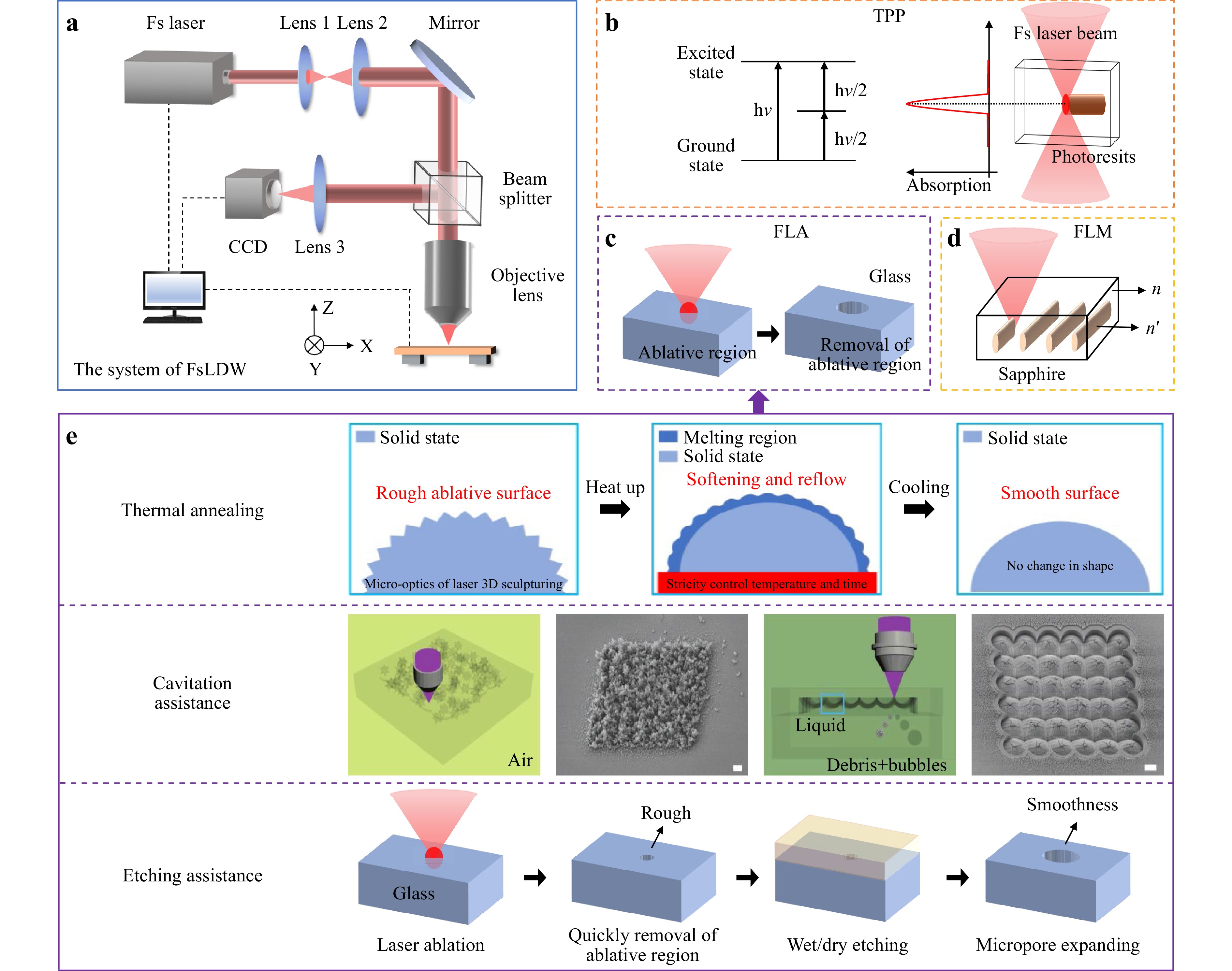
Fig. 1 Diagram of the femtosecond laser system and processing principle. a Diagram of the FsLDW system. The principle of b two-photon polymerization (TPP), c femtosecond laser ablation (FLA) and d femtosecond laser modification (FLM). e Assisted methods for FLA [obtained from ref. 71].
-
TPP is a unique photopolymerization micro-nano fabrication technique that utilizes the nonlinear effect of two-photon absorption to prepare 3D microstructures with characteristic dimensions beyond the diffraction limit64. In the single-photon absorption process, materials can only absorb a single photon with energy larger than their bandgap, achieving a transition from the ground state to the excited state. By contrast, when the incident light has a sufficiently high intensity, such as a femtosecond laser, materials can absorb two or more photons simultaneously to achieve an energy level transition. The energy of the femtosecond laser pulses conformed to a Gaussian distribution, which implies that the energy was the highest at the center of the spot and gradually decreased as the distance from the spot increased (Fig. 1b). Based on this theory, only the energy of a small area around the center of the spot can generate two-photon absorption. Therefore, processing accuracy with a sub-diffraction limit can be obtained using TPP65. In addition, TPP is a typical nonlinear process, and the probability of its occurrence is proportional to the square of the laser power66,67. Two-photon absorption can only be induced when the laser intensity exceeds a specific critical value, that is, the energy threshold. Leveraging this characteristic, the reaction area can be limited very near the focal point inside the material by focusing the femtosecond laser to realize true 3D processing.
-
The FLA is realized using the ultrahigh peak intensity and ultrashort pulse width of a femtosecond laser. For long-pulse lasers (e.g., >1 ns), the processing material has sufficient time to melt within the focused volume after being heated68. Meanwhile, the heat diffuses into the surrounding area, forming a thermal damage zone and resulting in poor processing quality. By contrast, when processing with ultrashort continuous femtosecond laser pulses, the pulse width is considerably shorter than the thermal diffusion time generated by coupling electrons and phonons. Therefore, the femtosecond laser can induce the rapid ionization of materials and produce plasma with high temperature, pressure, and density, thereby realizing the nonthermal ablation of materials and forming an ablation point depression (Fig. 1c). The nonthermal processing characteristic of a femtosecond laser ensures high-precision and high-quality processing of the material surface and maintains the stability of the optical, mechanical, and thermal properties of the material69,70.
To smooth the surface of an ablative machining structure further, combining auxiliary methods is necessary. The technologies of thermal annealing assistance71-74, cavitation assistance, and etching assistance (wet etching and dry etching75,76) are shown in Fig. 1e. Thermal annealing is typically used for amorphous materials such as glass77. Glass has no fixed melting point, and its transformation from solid to liquid occurs within a specific temperature range. By strictly controlling the thermal annealing temperature (≥1100 ℃) and time, only the glass surface is directly melted, and internal softening is minimized. The increase in the molecular kinetic energy on the surface, together with the microflow owing to the surface tension effect, produces a smooth surface similar to a liquid surface. Consequently, the surface quality significantly improved after cooling. The cavitation-assisted FLA is displayed in Fig. 1e (middle). The samples were covered with a liquid-filled recess to form an airtight environment. A femtosecond laser penetrates the material and focuses on the interface between the material and liquid. The ultrahigh peak power at the laser focus causes ablation of the material and cavitation of liquid bubbles78. The cavitation bubbles then pulsate and collapse on the sample surface, applying pressure to the ablative area, which can clean the ablated debris, resulting in a smooth surface79. Etching-assisted technology mainly consists of two steps: First, FLA is used to prepare the structure, and then, a suitable etching solution is selected to etch the processed area, reducing the surface roughness80. The surface roughness of an ablative structure is significantly reduced by using several auxiliary methods.
-
When a femtosecond laser is focused within a densely structured material, certain properties of the material in the focal region change after absorbing the laser energy; this process is defined as the FLM81-83. FLM does not change the shape of the material and is a unique processing mode of the femtosecond laser. After absorbing energy, electrons in the processing area are transferred to the lattice, and different types of modified structures are produced during this process. According to current research, FLM includes changes such as permanent refractive index changes, nonlinear coefficient changes, and fluorescence signal changes84-86. When the laser pulse energy reaches the modification threshold of the material, an isotropic refractive index change is generally formed within the material (Fig. 1d). The refractive indices of most materials increase after modification. When the pulse energy is further increased, a significant birefringence phenomenon occurs in the modified regions of materials such as quartz and borosilicate glass because of the formation of a lamellar nanogrid structure inside the material. The change in the refractive index caused by the FLM can be applied to the processing of 3D microoptical elements. The fabrication of optical devices using nonlinear photonic crystals is an important topic of research. FLM can modulate second-order nonlinear optical coefficients in the 3D space of crystals with excellent nonlinear optical properties (such as lithium niobate) and obtain 3D nonlinear optical elements87,88. Therefore, changes in the fluorescence signals (photochromism or photobleaching) of transparent materials by FLM can be used for 3D optical storage. Compared to traditional surface-embossed elements, 3D optical elements processed inside a hard material by FLM exhibit unique advantages in terms of wear resistance and stability.
-
In addition to selecting appropriate processing methods, other important design factors must be considered, such as strategies for achieving high efficiency, methods for converting data points from 3D models, and materials for microoptical elements. The following section will discuss these three aspects.
-
Generally, FsLDW uses a point-by-point processing method with a very small voxel, which is time-consuming when processing 3D structures with millions of pixels89,90. The single-point scanning mode of femtosecond lasers can no longer satisfy the requirements of efficient processing. Therefore, developing various methods to improve processing efficiency is essential.
-
The energy of the laser focus controls the size of the processing voxels. On the one hand, smaller voxels can be obtained to fabricate high-precision 3D structures by reducing the energy of the femtosecond laser. However, this requires extended processing time. On the other hand, high exposure energy leads to an increase in voxel size, which significantly reduces the processing time. However, this results in high surface roughness. Therefore, by taking advantage of small and large voxels, different voxel sizes can be combined for processing to meet complex requirements. For example, large voxels are used to fabricate a microoptical element base quickly, and small voxels are used to obtain a 3D structure with a smooth surface, as shown in Fig. 2a91. Two-photon grayscale lithography is a voxel modulation method that quickly and accurately modulates the irradiation dose through a single scanning plane92,93. This technique provides the high precision required for high-speed printing and manufacturing complex micropatterned structures.
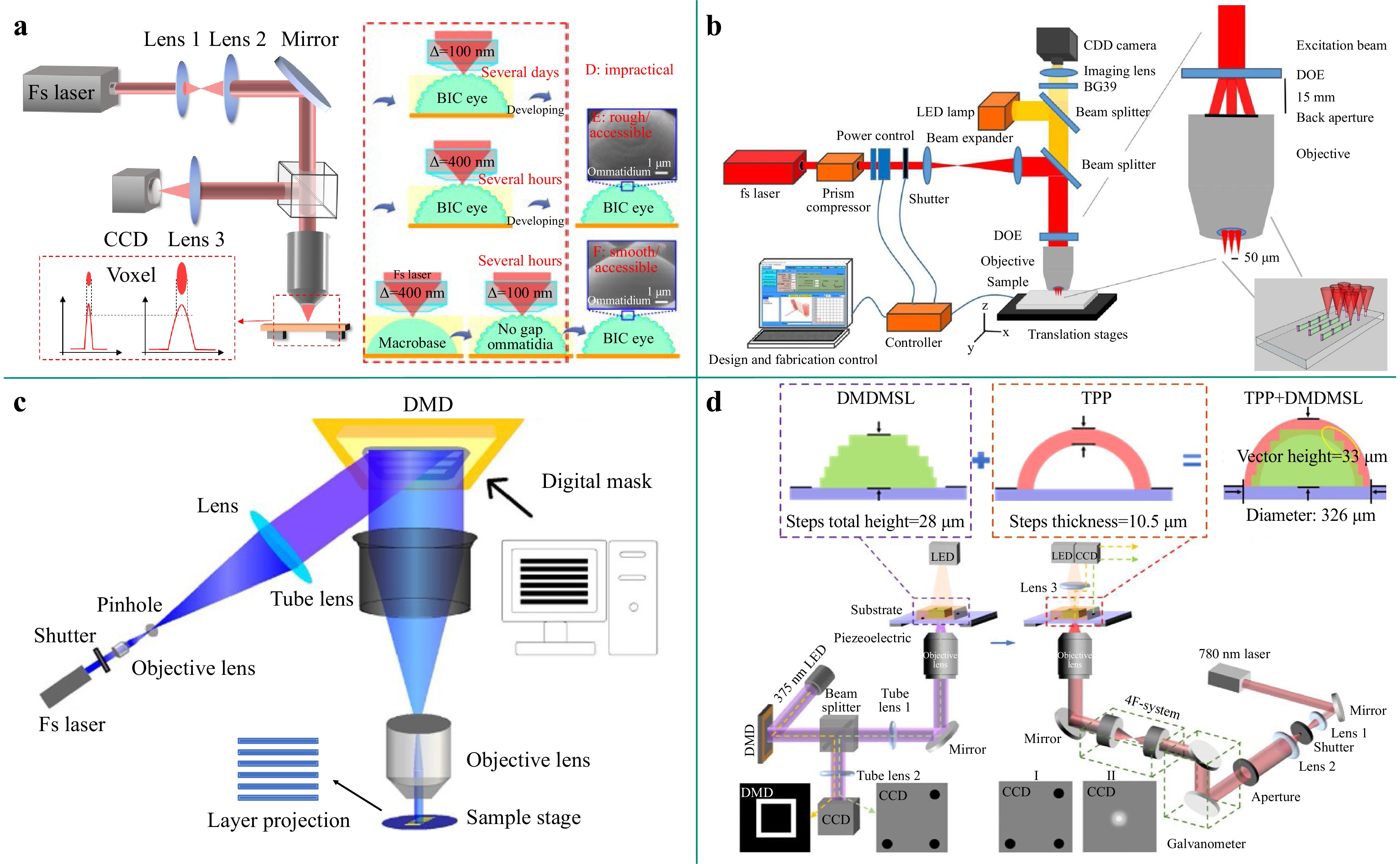
Fig. 2 a Processing method of high-speed voxel-modulation laser scanning (HVLS) [obtained from ref. 91]. b System of multiple-spot parallel processing (MSPP) with diffractive optical elements (DOEs) [obtained from ref. 99]. c Processing system of maskless optical projection nanolithography (MLOP-NL) based on digital mirror device (DMD) [obtained from ref. 102]. d Hybrid 3D printing method and system [obtained from ref. 105].
-
In addition to increasing the voxel size, the processing efficiency can be improved by increasing the number of femtosecond laser spots94-98. For example, Yang et al. established a multifocus TPP system based on a spatial light modulator (SLM)99. In their system, the laser beam completely irradiated the SLM with only phase modulation after passing through the beam expander. When computationally generated holograms (CGH) were loaded onto the SLM, the gray levels on the computational holograms modulated the 0–2π phase shift of the corresponding laser beam. Consequently, the femtosecond laser beam reflected from the SLM is modulated into multiple beams with a specific distribution, and multiple laser beams were subsequently focused on the platform to fabricate the structures. Maibohm et al. used diffractive optical elements (DOEs) to produce nine parallelized multibeamlets. The experimental setup is shown in Fig. 2b96. SLMs (such as microlens arrays (MLA) or DOEs) are introduced into TPP manufacturing systems through which the femtosecond laser beam can be split into tens or even hundreds of light points100,101. These methods enable parallel processing of the femtosecond laser to improve the processing efficiency.
-
Maskless optical projection lithography is a crucial technology in micro- and nanoscale graphics. Combining it with a femtosecond laser changes the point exposure mode to the planar exposure mode, significantly improving the processing efficiency. Liu et al. proposed and demonstrated an MLOP-NL system (Fig. 2c) for efficient cross-scale patterns102. The essential component of this system is a digital mirror device (DMD). The DMD modulates the laser beam by controlling the micromirror array, which produces a target exposure pattern for each layer. The MLOP-NL technology not only dramatically improves efficiency but also provides a powerful tool for fabricating multiscale integrated microsystems. Notably, the diffraction of the incident laser on the DMD and gap between the micromirrors results in significant energy loss, which requires a high laser power.
-
The collaborative use of multiple 3D printing technologies can improve processing efficiency and achieve cross-scale processing103,104. For example, Tan et al. combined the advantage of TPP and DMD micro stereolithography (DMDMSL) (TPP-DMDMSL) for hybrid 3D printing (Fig. 2d)105,106. The TPP system can produce voxels with a diameter of 400 nm; however, its processing efficiency is low. Conversely, the processing speed of the DMDMSL system is fast, but the minimum resolution is only ~1 μm. The two systems were used for different parts of the 3D structures with different precision requirements to balance the processing time and resolution. To fabricate the aspheric lens, the TPP method was used for the high-precision processing of the surface, whereas the internal steps of the lens without high precision were processed using DMDMSL. Because the two systems are independent, they mark the substrate with circular marks to enable the two systems to process on the same substrate. High-precision positioning was performed by identifying circular marks in the CCD. Overall, TPP-DMDMSL combines the high resolution and superior design flexibility of TPP with the rapid processing capabilities of DMDMSL for efficient, high-precision printing. Table 1 provides a comparison of the processing methods used in this study. Notably, the obtained spatial resolution varies depending on the processed material and the projection lens magnification of the femtosecond laser processing system.
Technology Light source Energy intensity Spatial resolution Characteristic Basic methods TPP Fs laser Low 10 nm-μm145 Nonlinear effect Single point scanning, low efficiency FLA Fs laser High 250 nm-μm70 Non-thermal ablation FLM Fs laser Medium ~1 μm85 Processed inside the hard material Highly effective strategies HVLS Fs laser Low 100 nm-400 nm91 Voxel-modulation, bigger voxels enhance efficiency MSPP Fs laser Medium 90 nm-μm263 Multibeam processing, parallelized processing enhance efficiency MLOP-NL Fs laser High 32 nm-μm102 Planar exposure mode besed on DMD High processing efficiency, can achieve cross-scale processing TPP-DMDMSL Fs laser and LED Low 500 nm-μm105 Multiple 3D printing technology synergy Table 1. A comparison of various FsDLW technologies.
-
Before processing, the 3D model must be translated into individual data-point coordinates, each of which is the location of a voxel107,108. During TPP, the femtosecond laser performs point-by-point processing according to the data points, and the processing area is photopolymerized to form a 3D structure. Because of its ablative properties, the data points used for processing in FLA are from structures that need to be removed. For the FLM, the area processed according to the data points was the laser-modified structural area. This section introduces a method for transforming a 3D model into data points. Notably, given the various efficiency improvement methods in section of “Strategies for achieving high efficiency, the methods of transforming the 3D model into data points need to be adjusted accordingly.
-
In general, we convert the entire structure of the printed model into data points. During the conversion, the 3D model must be converted into a layer-by-layer 2D plane structure, where each layer is a single 2D data point (i.e., X and Y coordinate points). We also need to get the $ \text{Z} $ coordinate of each 2D plane structure, which is called slicing. The slicing process generally uses the equal-height slicing method109,110, which refers to an equal distance between each layer of a 3D model. However, for 3D curved microstructures (such as optical lenses and spherical microstructures), the thickness of the slice is a key factor that determines the surface quality. An image of the lens surface obtained by equal-height slicing with a layer spacing $ \text{h} $ of 100 nm is shown in Fig. 3b. Apparent solenoid traces are observed owing to the lateral offset of the voxel position, particularly at the top of the lens. This lateral offset has a significant effect on the roughness of the lens surface. Therefore, equal-height slicing is not an effective method for dealing with 3D microstructures of lenses. An equal-arc slicing method has been proposed to compensate for the large offset of voxels in the equal-height slicing method111-113, which implies that the layer height $ {\Delta }{h = \Delta L}\text{}\text{×}\text{}\text{sinθ} $ is variable. $ {\Delta }\text{h} $ depends on the arc length ${\Delta }\text{L} $ and sloping angle ${θ} $. A microlens with a smooth surface is obtained by selecting an appropriate arc for the isoarc slicing.
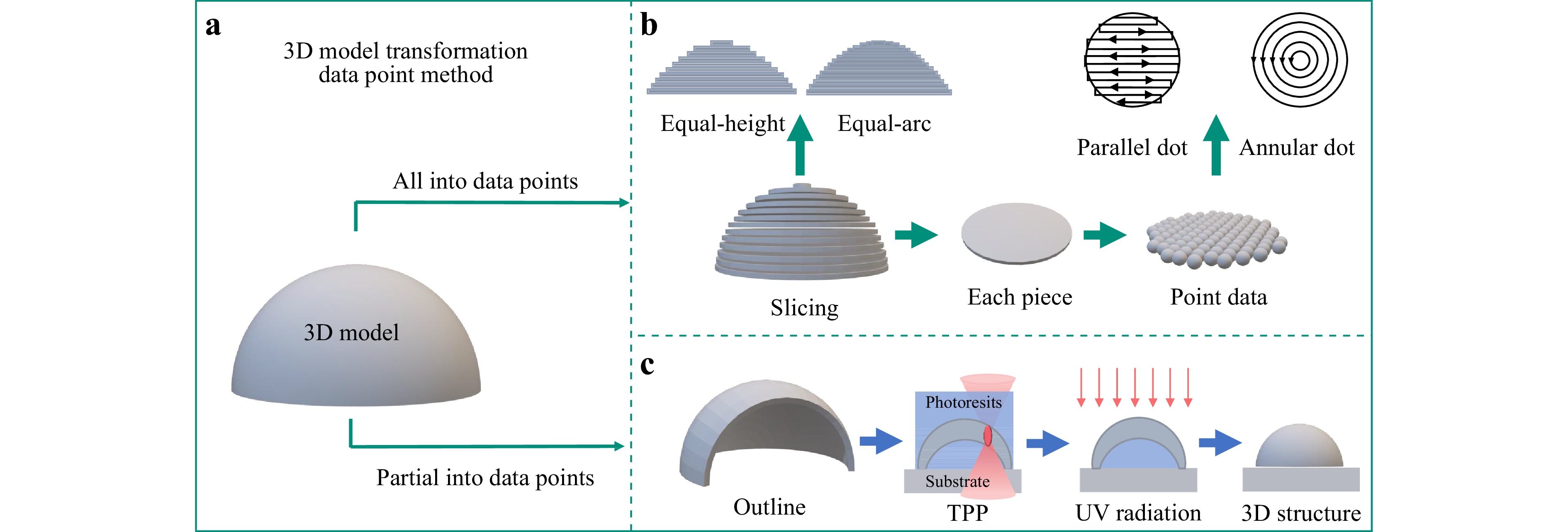
Fig. 3 a 3D model transformation data point method. b All 3D models are converted into data points. c 3D models are converted into data points partially.
Then, we transformed each 2D slice into a series of points containing $ \text{X} $ and $ \text{Y} $ coordinates114,115. The 2D slices are generally transformed into parallel point coordinates that are suitable for most microstructures. However, because each layer of the microlens exhibits a circular structure, the lines formed by the coordinates of parallel points not only distort the outline of the circle but also create some protrusions on the edges of the lens surface. Therefore, to obtain optical elements with smooth edges, annular point coordinates are generally chosen to ensure circular symmetry and radial consistency of the lens.
-
To obtain a reduced number of data points, the 3D model can be partially (i.e., the contour) converted into data points116,117 (Fig. 3c). During TPP, the voxel size can be controlled by changing the laser power or scanning speed to create a shell with sufficient mechanical strength114. The unpolymerized portion of the outer layer of the contour was then removed by developing. Finally, the inner part of the contour is irradiated with UV light to obtain a completely polymerized structure. The fabrication of the shell, development, and post-processing with UV light significantly reduced the processing time. However, the contour scanning method requires a processed material with high mechanical strength. Otherwise, the development causes the collapse of the polymerization contour, resulting in processing failure. For FLA processing, detaching the part outside the target structure is also possible by processing only the contour data points.
Two types of data point conversion methods are available for single-point scanning processing, which are the most basic data point conversion methods. To improve the efficiency of the different processing methods mentioned in section of “Strategies for achieving high efficiency”, we need to improve the data point conversion methods correspondingly. For example, we need to modify the distance between voxels for HVLS. In the case of the MSPP, the SLM needs to be controlled to generate multiple focuses. For the MLOP-NL, the data points must be modified to the plane projection data of the DMD. In the hybrid 3D printing method, models and data points must be split.
-
Materials suitable for optical element processing can also be categorized according to the three optical element processing methods in FsLDWs. The first is photopolymerization materials applicable to TPP, which mainly include polymeric materials and organic-inorganic hybrid materials118. Polymeric materials include resins119-123, polydimethylsiloxane (PDMS)124, and proteins125,126. Organic–inorganic hybrid materials include silicon nanocomposite127-129, sol–gel glass130,131, and polyhedral oligomeric silsesquioxane (POSS) glass materials, which can form glass after heat treatment132,133. Second, hard and brittle materials with excellent stability and optoelectronic properties are suitable for FLA, including crystalline (sapphire and silicon) and noncrystalline (glass) materials. The materials used for FLM include glass, crystalline materials, graphene, and hydrogels, which partially overlap with the materials used for FLA. A partial overlap occurs between photopolymerized and ablative materials, such as certain photoresists and other polymeric materials that can be processed by both photopolymerization and laser ablation. However, the ablation process usually results in high surface roughness, which cannot meet the high-precision requirements of optical elements. By contrast, the structures obtained by photopolymerization exhibit smoother surfaces with smaller voxels134,135. Therefore, overlapping materials are primarily processed using photopolymerization. The classification and corresponding auxiliary processing methods for the processed materials are shown in Fig. 4.
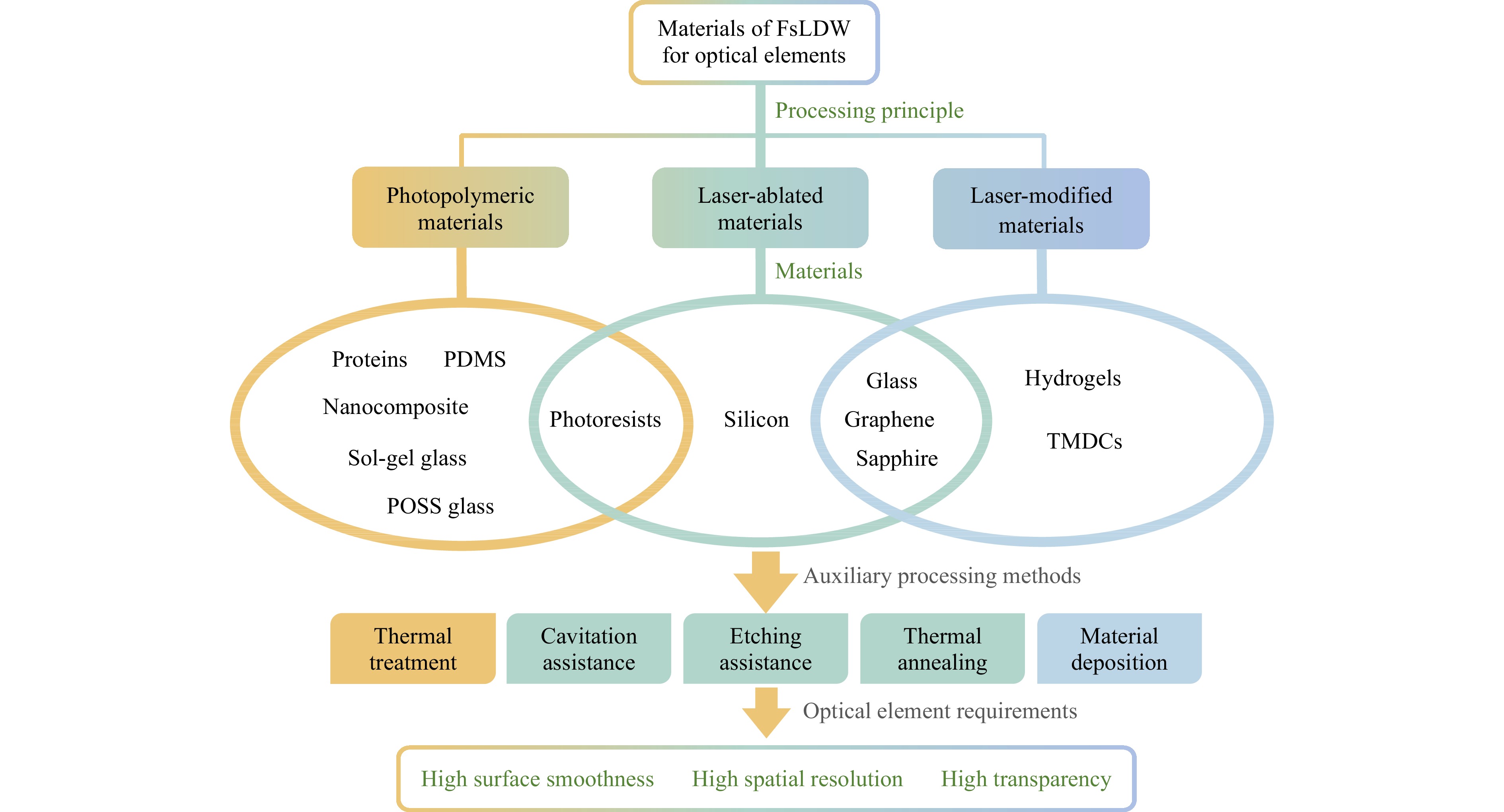
Fig. 4 Various materials for fabricating microoptical elements using FsLDW and their auxiliary processing methods.
-
Various photopolymerization materials are suitable for TPP. Several resin materials can be self-configured, the advantage of which is that the ratio of each part of the material can be adjusted according to the device requirements to obtain the best printing results. In addition, mature commercialized photoresists and other resin materials can be purchased. The commonly used photoresists are the SU-8 series125 (manufacturer Microlithography Chemical) and IP series120. SU-8 is a near-UV photoresist based on an epoxy resin (from the rubber industry), which exhibits excellent imaging properties. Owing to its low absorption in the wavelength range of 365–400 nm, each layer of SU-8 can obtain uniform exposure. Therefore, it can process thick-film structures with vertical sidewalls and high aspect ratios. IP series photoresists have a wide variety of IP series photoresists, mainly IP-S and IP-n162. The optical, mechanical, electronic, and biological properties of these photoresists were engineered to make them suitable for optical, optoelectronic, and biomedical applications.
Commercial bovine serum albumin (BSA, aqueous solution) was used to process the optical microdevices. When methylene blue is used as a photosensitizer, the absorbed laser energy is transferred to ground-state oxygen, forming reactive oxygen species such as singlet oxygen. Singlet oxygen can easily catalyze the inter- or intramolecular covalent crosslinking of oxidizable protein residues (such as Tyr, Trp, and His), forming a 3D protein microhydrogel125,126. After processing, proteins at higher concentrations (400–500 mg/mL) can achieve a more robust mechanical structure. The natural structure of a protein undergoes reversible conformational isomerization at different pH values. Microoptical elements processed with proteins have flexibility and extensibility, as well as good biocompatibility and biodegradability.
PDMS exhibits 100% light transmittance and is an ideal hydrophobic silica gel material for processing optical elements124,136. PDMS is nontoxic, odorless, physiologically inert, chemically stable, electrically insulating, weather-resistant, soft, and can be processed into soft lenses. Moreover, PDMS is highly sensitive to organic solvents, and most organic solvents diffuse into PDMS materials, leading to material expansion. Solvent-tunable PDMS microlenses are fabricated by exploiting the solvent responsiveness.
Some of the aforementioned soft materials have poor robustness and are unsuitable for use in extreme environments (such as strong acids, strong bases, and high temperatures). Hard materials such as quartz glass are the materials of choice for several high-performance elements in optics because of their high optical transparency and high thermal, chemical, and mechanical stability137. Fused silica microstructures are particularly attractive for optical and biomedical applications. Fused silica glass can be fabricated by firing some organic-inorganic hybrid materials. Three major types of organic–inorganic hybrid materials, including silica nanocomposites, sol–gel glass, and POSS glass materials, can be processed into glass by TPP and heat treatment. The first type is a mixture prepared by adding silica nanoparticle fillers to photopolymer precursors127,138,139. Photopolymerization precursors generally consist of two main components: small-molecule polymeric monomers and large-molecule crosslinkers. On the one hand, polymeric monomer solution allows the dispersion of large amounts of silica nanoparticles, while crosslinker can provide more chemical bonds for photopolymerization. By contrast, the polymeric monomers and crosslinkers exhibit different refractive indices. By adjusting the ratio in the solution, the overall refractive index can be made very close to that of silica. This reduces the scattering of light spots during processing, thereby improving the processing resolution. After curing by TPP and thermal degreasing and sintering (>1100 ℃), silica nanocomposites can be transformed into fused silica glass, achieving a resolution of several hundred nanometers and a surface roughness of several nanometers140. Glass ceramics are formed from silica nanocomposites at precisely controlled temperatures (~1200 ℃) during sintering, which exhibit superior optical properties compared to ordinary glass materials, such as better robustness and lower scattering141,142.
Unlike silicon nanocomposites, sol–gel glass materials do not require such high heat treatment temperature130,143,144. The sol–gel method uses inorganic salts containing silica as precursors, which are then gradually gelated through hydrolytic condensation. Finally, sol–gel glass materials (also known as liquid glass) were obtained after post-treatment and drying. Because the inorganic silica filler is introduced at the molecular scale by mixing the precursors, it allows the incorporation of silicon groups to control the homogeneity of the material better; thus, the particle cluster problem does not arise130. In addition, these precursors contain a photopolymerizable fraction (acrylate or epoxy resin). The sol–gel material was photocured using TPP to form a 3D structure. Then, it was degreased and sintered at 600 ℃. 3D structures with glass as the main body can be formed after cooling. Owing to the low heat-treatment temperature, sol–gel materials can be used to fabricate structures on the surface of devices that are not resistant to high temperatures. With the continuous development of sol–gel glass materials, further reducing the processing temperature and broadening the application scenarios is possible145.
Another material that can be converted into fused silica at low temperatures (650 °C) is POSS glass145,146. The POSS glass consists of three components: 89 wt% acrylate-functionalized POSS monomer, 9 wt% trifunctional acrylic monomer, and 2 wt% photoinitiator of the α-aminoketone family. POSS is an organic–inorganic hybrid polymer consisting of a caged silicon–oxygen framework147,148. When sintered into a solid, POSS exhibits a better high-temperature resistance and robustness than most pure organic polymers. Long-armed, branched trifunctional acrylic provides important resilience against cracking, which is the key to printing structures with sufficiently dense silica-oxygen nanoclusters at a low temperature (650 °C). Furthermore, the viscosity of the resin can be regulated by varying the concentration of the trifunctional acrylates. The photoinitiator exhibited a high quantum yield for generating free radicals when excited at the 780 nm wavelength of the TPP system, thereby facilitating efficient polymerization of the materials. Overall, POSS glass materials exhibit excellent optical properties, mechanical elasticity, ease of processing, and high spatial resolution (down to 10 nm), which are suitable for the micro- and nano-3D printing of optical elements.
-
Hard and brittle materials are also known as difficult-to-process materials, and their complex, brittle, and stable characteristics render fine processing much more complicated than that of ordinary materials75,149. Moreover, hard and brittle materials contain many material systems, and materials composed of different atoms exhibit significant differences in their physical and chemical properties. Other micro- and nanoprocessing techniques are challenging to apply to hard, brittle materials. Owing to the instantaneous high-intensity energy of the femtosecond laser, high-precision machining of hard and brittle materials can be achieved using FLA combined with several auxiliary methods in section of "Processing principle of FLA". Graphene oxide150-152, optical glass137,153,154, and crystals (such as sapphire 71,155 and silicon146,156-158) are the most widely used laser-ablative materials. These materials have excellent physical and chemical stabilities, including high hardness, high-temperature resistance, and corrosion resistance, and are widely used in extreme fields, such as the military and aerospace industries. They also have critical applications in microoptics and microelectronics, owing to their broad spectral transmittance, nonlinear optics, and other optoelectronic properties. Their combination of functionality and stability make them ideal materials for preparing micro- and nanooptical devices. For instance, except for diamonds, sapphire is the hardest natural mineral on Earth. Sapphire glass has excellent thermal properties, infrared transmission properties, and good chemical stability. Therefore, it is often used to fabricate optical elements and infrared-transparent optical windows and is widely used in infrared and far-infrared military equipment. Graphene is a novel material composed of carbon atoms arranged in a tightly packed single layer with a 2D honeycomb lattice structure that exhibits exceptional optical, electrical, and mechanical properties. Graphene is one of the most robust materials and is ductile and bendable. It holds significant potential for applications in micro- and nanoprocessing, materials science, energy, and biomedicine.
-
Some laser-ablative materials such as glass, crystals, and graphene oxide82,150 can also be used as laser-modified materials. Glass and crystalline materials exhibit good light transmission, and FLM can change their refractive indices, absorption coefficients, nonlinear optical sensitivities, and crystal structures159. Graphene oxide turns into reduced graphene oxide under laser irradiation, and its optical properties significantly change during this process160. The optical reduction also results in much higher refractive index modulation ($ \text{Δn} $ of ~0.8) than conventional optical materials161. 2D layered materials generally refer to graphene and transition metal dichalcogenides (TMDCs) MX2, where M is a transition metal atom (such as Mo and W), and X is a chalcogen atom (S, Se, or Te)162-165. Nanoparticles can be generated in single-layer TMDC crystals using femtosecond lasers to obtain amplitude or phase modulation by strong scattering of incident light166. 2D layered materials with sufficient phase or amplitude modulation can be processed into ultrathin lenses that can reach the thickness of a single atom167.
In addition to the aforementioned materials, which can be directly fabricated into optical elements after modification, some materials, such as hydrogels, require post-treatment after modification. Femtosecond lasers can alter the polymer network of polyacrylate–polyacrylamide hydrogels in pure water, thereby reducing scaffold density and improving the ability to form hydrogen bonds168. Hydrogels can trap various materials through different interactions, including hydrogen bonds, charge effects, or dense scaffolds169,170. Therefore, various materials, such as metals, 2D materials, molecular crystals, semiconductors, biomaterials, and fluorescent substances, can be assembled onto hydrogels to form 3D structures. Moreover, to achieve processing resolutions below the diffraction limit (20–35 nm), pretuning the properties of the patterned gel before material deposition is necessary.
-
Owing to the aforementioned processing advantages, FsLDW technologies are widely used to fabricate various imaging/nonimaging microoptical elements. Microoptical elements are categorized into refraction, reflection, diffraction, and hybrid-principle microoptical elements according to their control capabilities over light, each of which can be further divided into imaging/nonimaging microoptical elements. In this section, we provide a detailed description of the microoptical elements.
-
Refractive microoptical elements (such as microlenses and arrays) are widely used in various microoptical systems171-173. As an important type of refractive microoptical element, microlenses play an irreplaceable role owing to their small size, light weight, and excellent optical properties, particularly in the fields of beam shaping and imaging174,175. Xu et al. used TPP and SU-8 to process a concave–convex microlens (CCML) consisting of two different high-curvature surfaces176, as shown in Fig. 5a. The CCML provides greater design flexibility and significantly enhances the optical performance, including aberration reduction. Sun et al. used bovine serum albumin (BSA) to process protein microlenses (Fig. 5b)126. When the protein microlens is stimulated by chemical signals, the microstructures exhibit rapid and reversible expansion and contraction. Thus, the focal length of the fabricated microlenses could be regularly and reversibly tuned through pH modulation. Owing to their tunable properties and complete biocompatibility, protein microlenses demonstrate significant potential in optical, electronic, and biomedical applications.
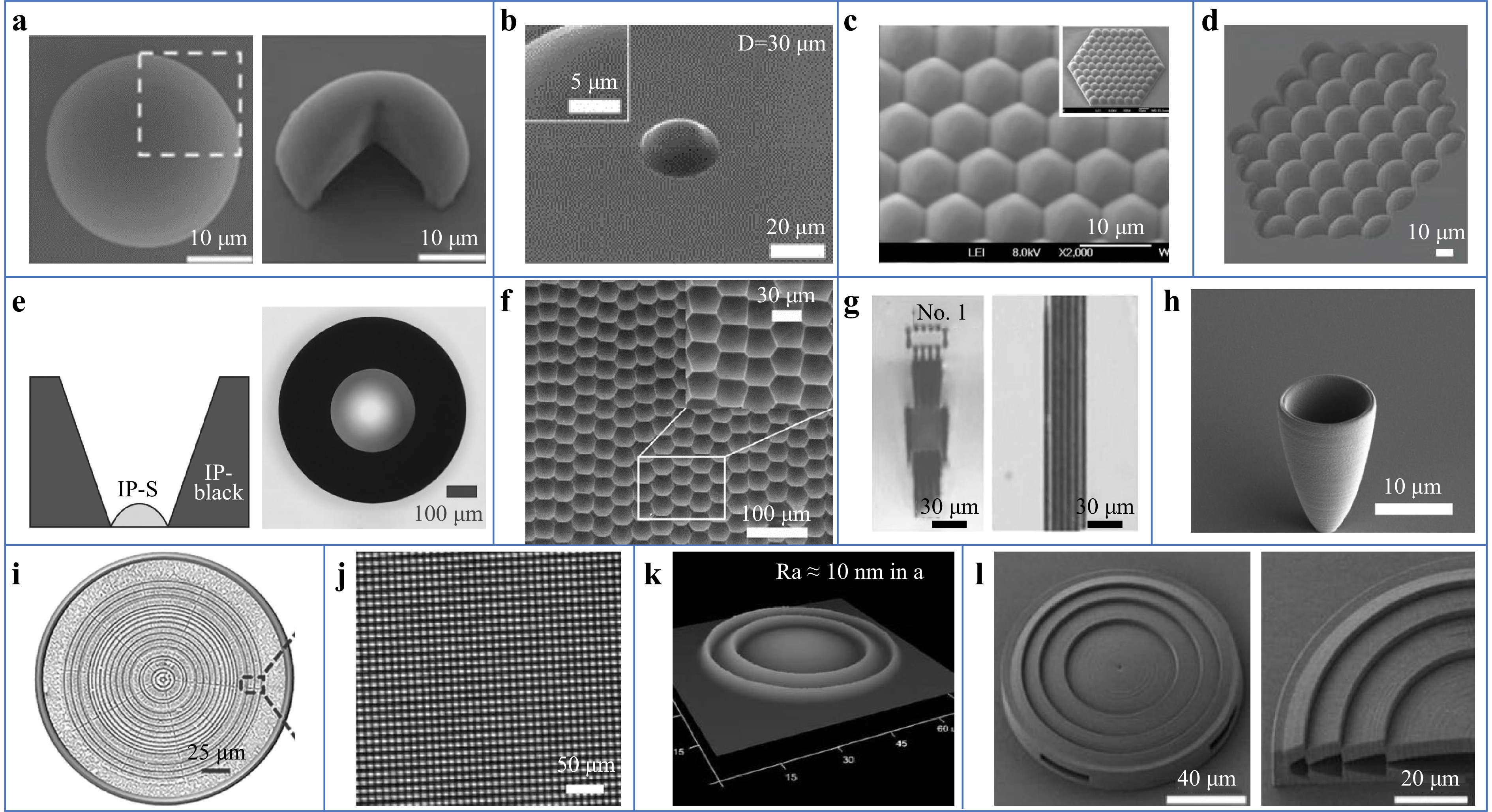
Fig. 5 a–e Refraction in the microoptical elements. a SEM image of concave–convex microlens (CCML) [obtained from ref. 176]. b Protein microlens [obtained from ref. 126]. c High-quality microlens arrays (MLA) with designable Nas [obtained from ref. 111]. d MLA with high numerical aperture (NA) [obtained from ref. 71]. e Prototype IP-Black aperture and lens made from IP-S [obtained from ref. 179]. f–h Reflection micro-optical elements. f Large-area concave all-silicon MLAs [obtained from ref. 157]. g Rectangular depressed-cladding waveguides written by the femtosecond laser in 6H–SiC crystals [obtained from ref. 182]. h 3D microphoton parabolic beam directors [obtained from ref. 183]. i–l Diffractive microoptical elements. i SEM image of the metalens [obtained from ref. 196]. j Custom volume gratings (grids) [obtained from ref. 192]. k Protein hydrogel-based continuous relief harmonic diffraction microlens [obtained from ref. 201]. l Multilayer diffraction structure [obtained from ref. 106].
Close-packed MLA with high NA is suitable for high-resolution imaging177,178. Wu et al. successfully fabricated high-quality MLAs using an equal-arc scanning strategy111 (Fig. 5c). The fill rate of the MLA was ~100%, and the NA was 0.46, which is much higher than the reported value of 0.13. The fabricated MLA exhibits high-resolution imaging capabilities. Hua et al. used FLA- and cavitation-assisted methods to prepare convex MLAs (Fig. 5d) with a fill factor of up to 100% on sapphire crystals, which is difficult to achieve using other techniques71. This technology allows the manufacture of MLAs of arbitrary sizes, curvatures, and surface types.
Schmid et al. described a novel and easy method for creating 3D-printed opaque structures using a highly absorptive photoresist. This technique can be employed for the production of microscopic apertures, contrast enhancement in 3D-printed microoptical elements, and realization of novel optical designs179. The hybrid design shown in Fig. 5e features a solitary IP-S lens and an IP-black diaphragm. The integration of black photoresists enables more complex optical designs and can effectively improve the imaging quality of optical elements.
-
Compared with refractive microoptical elements, reflective microoptical elements have the advantage of inherent achromatic properties180. Three categories of reflective optical elements are processed using FsLDW. The first is an optical element processed using a femtosecond laser, which inherently exhibits a good reflective surface. Deng et al. used a single-pulse femtosecond laser wet etching (SP-FLWE) technique to fabricate large-area concave all-silicon MLAs157 rapidly. This method can produce approximately three million microlenses with parabolic profiles within 1 h (Fig. 5f). In addition, because the microlens height and aperture exhibit an approximately proportional relationship with the laser scanning speed, MLA of different sizes can be easily obtained by varying the laser scanning speed. A reflective homogenizer MLA with a fill factor of 99% was tested using a He–Ne laser. The results reveal that the output beam through the MLA has a uniform light intensity distribution. Because of their transparency in the infrared region, these concave silicon MLAs can be extended to infrared light for homogenization.
The second type is the total internal reflection (TIR) optical element processed using the total reflection principle. Bianchi et al. prepared a microparabolic reflector using a photocured resin consisting of a diacrylate monomer181. The center of the structure was a sphere centered at the focal point of the paraboloid. Because of total internal reflection, the light propagating inside the outer fiber core was reflected by the lateral parabolic surface. In this structure, the reflected light was incident perpendicular to the sphere, minimizing the deflection owing to refraction. In addition to the large NA, parabolic reflectors can also focus independently of the submerged medium because they do not depend on refraction. A waveguide (lightguide) is a reflective microoptical element modulated by the refractive index that utilizes the principle of total internal reflection to guide light along a specific path efficiently. It demonstrates extensive applications in integrated optoelectronic devices. Various waveguide structures based on transparent materials have been prepared using the FsLDW technology, including single-, double-, vertical-dual-line, multiple-line, ridge, and depressed claddings. Zhang et al. prepared double-line and depressed-cladding waveguides in 6H-SiC (silicon carbide) crystals using the FLM (as shown in Fig. 5g)182. The mode distribution could be adjusted by changing the processing parameters of the waveguides. Their study provided a method for manufacturing low-loss waveguides in 6H-SiC crystals, which is important for future SiC-based integrated quantum photonics.
The last category involves the deposition of metals onto the surface of an element to form reflective optical elements. Atwater et al. used a femtosecond laser to produce 3D microphoton parabolic beam directiors183 (Fig. 5h). After coating with 20 nm chromium and 380 nm silver using a plasma sputtering coater, the optical aperture was etched to the bottom of the paraboloid using focused ion beam lithography. Finally, a set of micron-scale silver-coated 3D paraboloid structures was obtained and anchored to the silver-coated substrate at the bottom of the paraboloid. Microphoton parabolic light directors can be used to design the collimating beam of advanced solar cells and LED.
-
Diffractive microoptical elements (DOEs) are divided into harmonic diffractive optical elements (HDOE), single-layer diffractive optical elements (SLDOE), and multilayer diffractive optical elements (MLDOE)184-187. DOEs use the 3D relief structure of their surfaces to modulate and transform the wavefront phase and are characterized by lightness and thinness, design flexibility, free modulation of the incident light, and batch reproducibility122. Compared to conventional refractive and reflective optical elements, DOEs can simplify structures, reduce weight and volume, and improve the imaging quality of conventional optical systems188,189.
Various SLDOEs have been successfully fabricated over the last few years190. Based on BSA and PDMS, Sun et al. fabricated a new soft diffractive microoptical element using the TPP technique, named microscale kinoform phase-type lens (micro-KPL)191. Even in strongly acidic or alkaline environments, micro KPL offers excellent surface quality, precise 3D shape, and unique optical properties. Using sol–gel materials and TPP technology, Hong’s team prepared a single-sided diffraction grating with a linear shrinkage of 17% after heat treatment at 600 ℃130,192. The 3D printing of glass microoptical elements with isotropic shrinkage, micron resolution, low peak-to-valley deviation (<100 nm), and low surface roughness (<6 nm) can be achieved in this manner.
Lin et al. reported a method for converting 2D monolayer materials into ultrathin flat lenses using FLM166. Sufficient phase or amplitude modulation can be obtained by generating a localized scattering medium within a monolayer of material via the FLM. Efficient 3D focusing can be realized through subwavelength resolution and diffraction-limit imaging, which allows diffraction-limit imaging at different magnification rates at different focal locations. Ultrathin lenses with subwavelength thicknesses are promising alternatives to conventional refractive lenses and demonstrate potential applications in miniaturized and compact imaging systems193-195. Wei et al. used the FLA method to demonstrate a broadband zoom graphene metalens with a thickness of 250 nm, which covers the entire visible spectrum (Fig. 5i)196. The fabricated graphene metalens enabled continuous and simultaneous adjustment of the focal length of light with different wavelengths. Laterally stretching the lens, a focal adjustment range of >20% can be achieved for three wavelengths (650, 550, and 450 nm).197,198. Laser-modified hydrogel materials are used to produce volume and subsurface diffraction gratings192. Densification of the hydrogel was achieved by controlling the laser power, speed, and penetration depth, and relevant changes in the local refractive index (RI) were described. Variations in RI facilitated the processing of customized volume gratings (parallel lines, grids, squares, and ring gratings) in the hydrogel (Fig. 5j).
A conventional single-layer DOE can achieve 100% diffraction efficiency only at the designed wavelength. Because of the severe wavelength dependence, the diffraction efficiency decreases substantially with the deviation in the incident wavelength. The HDOE, proposed by Dean Faklis et al., is characterized by the requirement that the optical path length between adjacent surfaces be an integer multiple of the design wavelength λ0199. HDOE can obtain the same focal length at a series of separated wavelengths, effectively eliminating imaging chromatic aberration, and is widely used in infrared imaging systems200. Sun et al. constructed a protein-based harmonic diffraction microlens (PHDM)201, as shown in Fig. 5k. With the excellent 3D morphology provided by the TPP, the PHDM exhibits remarkable harmonic diffraction optical properties and good focusing and imaging performance. Because of the irritability of the protein molecule, the focal length of PHDM can be easily adjusted in a few seconds by changing the pH value (focal length tunability of up to ~20%), resulting in unique pH-responsive behavior and good biocompatibility.
Arieli et al. proposed the design of microstructures with different concave and convex shapes by matching and combining two diffraction elements with different dispersion coefficients, which is defined as MLDOE. Thus, aberrations can be eliminated in a broad spectrum depending on the different phases required for different combinations. Hu et al. fabricated an SU-8 microstructure with an arbitrary continuous surface and high precision using TPP188, as shown in Fig. 5l106. The wideband operating characteristics of MLDOE can achieve an average diffraction efficiency of >84%, which is maintained above 80% over the entire visible band (406–824 nm). With the rapid development of integrated quantum photon technology, the design and preparation strategies for wideband MLDOEs have attracted considerable attention and are widely used.
-
Compared with single diffractive optics, HOE exhibits unique dispersion, excellent thermal properties, monochromatic aberration correction capability, and wavefront correction capability, which can improve the design flexibility and overcome several limitations of conventional optical elements. HOE can be divided into hybrid refractive–diffractive optical elements (HRDOE) and hybrid refraction–reflection optical elements (HRROE). The HRDOE exhibits several advantages over conventional optical elements in improving image quality188, reducing size and cost. Hua et al. designed and fabricated a hybrid diffractive refractive lens (HDRL) using FsLDW202. As shown in Fig. 6a, the diffractive section is an achromatic element with a diameter of 10 mm situated within a Z-cut sapphire substrate, whereas the refractive portion consists of a spherical plano-convex lens. HDRL exhibits superior imaging performance in terms of the modulation transfer function compared to a single spherical lens. Fabricating diffractive elements inside the spherical lens not only further improves the thermal stability of the optical system but also reduces its size and weight. Tian et al. proposed a small and simple optical vortex beam generator called a hybrid refractive–diffractive optical vortex microlens (HOVML)203, as shown in Fig. 6b. A helical dislocation plate was integrated into a normal SU-8-based microlens using TPP. The HOVML generates optical vortex beams using only one refractive–diffractive hybrid microlens. The optical properties of the HOVML simulated in the far field agreed with the experimental results. Moreover, the theoretical conversion efficiency of the HOVML is higher than that of multienergy and amplitude-type diffractive elements owing to its continuous surface structure. Optical vortex beams have promising applications in various fields, such as optical communication, quantum information, and astronomy.
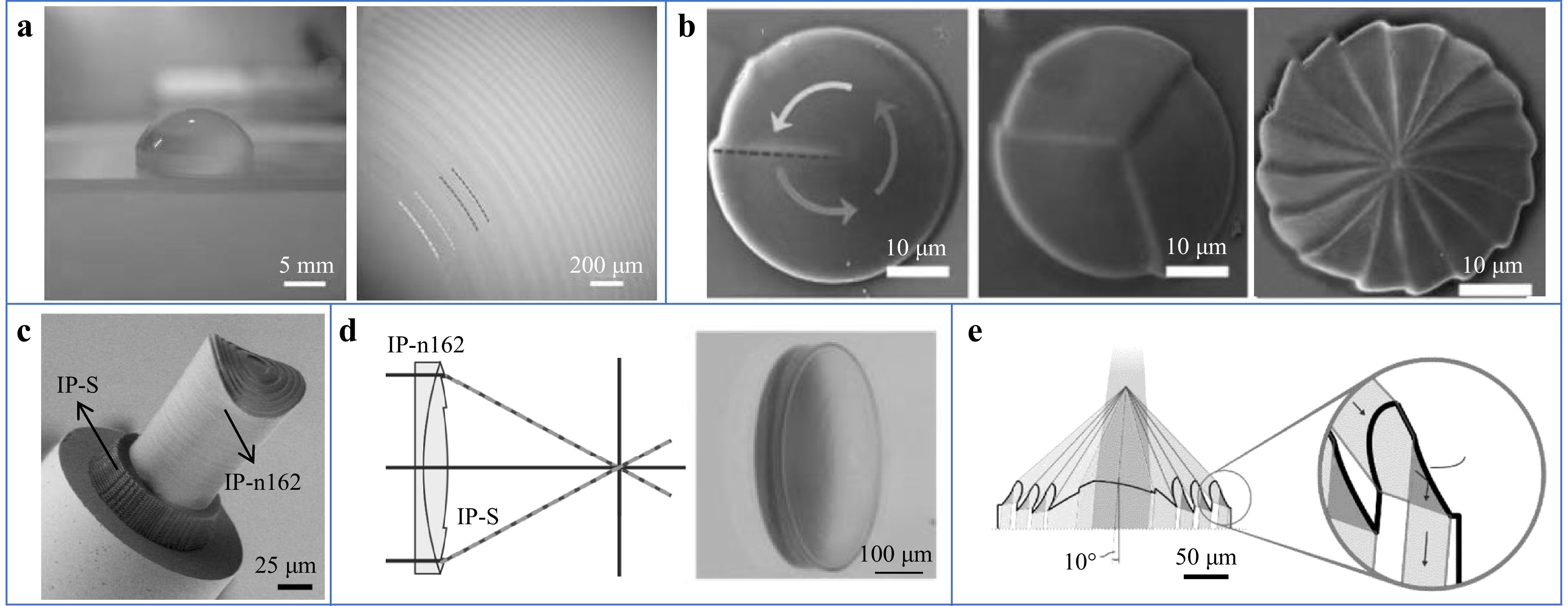
Fig. 6 a Achromatic element inside a Z-cut sapphire wafer [obtained from ref. 202]. b Highly integrated hybrid refractive–diffractive optical vortex microlens (HOVML) [obtained from ref. 203]. c Polarization control and beam shaping on a fiber [obtained from ref. 204]. d Achromatic lens is made of two materials [obtained from ref. 121]. e Hybrid refraction and total internal reflection lenses [obtained from ref. 205].
Multimaterial HRDOE exhibits more abundant functions than single-material elements, such as excellent achromatic properties. Timo et al. processed a hybrid material system using two different photoresists (Fig. 6c)204. They first used IP-Dip to fabricate chiral photonic crystal structures on the end faces of optical fibers as circularly polarized filters. The HRDOE was fabricated using the IP-S, which consisted of saddle-shaped free-form lenses with Fresnel zone plates (FZPs) on top. With photonic crystals and an HRDOE, the system is capable of both polarization control and beam shaping. Michael et al. processed optical elements with excellent achromatic properties using two materials (IP-S and IP-N162), as shown in Fig. 6d121. The apochromat includes a refractive aspherical portion and step portion of the diffractive surface. IP-N162 and IP-S were used to prepare the base and the top of the apochrome, respectively. The apochromatic/achromatic lens exhibits design flexibility and can be used at different wavelengths, such as 500, 600, and 700 nm. Li et al. investigated an HRROE suitable for high-NA side-viewing configurations to capture fluorescent emission light205. In the TIR lens, light undergoes TIR and is directed toward each of its ‘teeth,’ where it is refracted on the second surface (Fig. 6e). Leveraging the degrees of freedom associated with reflection and refraction within a confined space enables an exceptionally compact design.
-
Stereoscopic systems are integrated systems formed by multiple optical elements combined in the horizontal or vertical direction and are widely used in optoelectronics206, biomedicine207-209, robotics, and microfluidics210. The optical elements in a stereo system are connected via auxiliary structures, all of which are processed using a femtosecond laser. This section focuses on the auxiliary structures and several typical imaging/nonimaging applications of stereoscopic systems. Imaging applications include integrated imaging systems, imaging systems combined with microfluidics, and imaging systems for optical storage. Nonimaging applications include optical modulation systems, spectral inspection systems, and waveguide-based photonic chip systems.
-
Processing auxiliary structures is necessary in addition to developing individual optical elements. For example, when processing a system with multiple elements, auxiliary structures are required to connect multiple optical elements (as shown in Figs. 7a−c). These auxiliary structures are processed directly during the fabrication of the optical elements. Thus, they can be used to precisely locate the distance between elements. To facilitate the combination of optical elements and fibers, an auxiliary structure called a fiber chuck was proposed by Parvathi (Fig. 7d)211. One end of the fiber chuck was integrated with optical elements, and the other end was designed as a structure that could be inserted using optical fibers. In addition, another structure in the chuck limits the insertion depth of the optical fiber, reducing manual alignment and distance errors. Auxiliary structures are also suitable for elements that undergo deformation during processing. For example, processing structures based on organic and inorganic hybrid glass materials along with the glass substrate must be heat-treated after TPP, during which the structure shrinks and deforms. Therefore, designing precompensated deformation structures is necessary. As shown in Fig. 7e, the precompensation structure between the optical element and glass substrate prevents distortion of the element. Fig. 7f shows the PDMS-based auxiliary structures with elastic deformation191. Protein optical elements processed on PDMS substrates demonstrate good elasticity and scalability. Auxiliary structures also help improve the imaging quality, such as apertures. Tan et al. designed and processed a simple double-sided microlens system using SU-8 (Fig. 7g)212. They plated an opaque metal film on one side of a glass substrate to form an aperture. By integrating the aperture as an auxiliary structure into the system, excess light can be prevented from entering the lens, effectively improving the imaging quality. Weber et al. produced an aperture in a 3D-printed micrography system using Ag shadow evaporation51. Commercially available rust solutions can oxidize Ag films to produce a low-reflectance layer that can serve as an excellent aperture. The combination of optical and auxiliary structures can expand the number of functions.
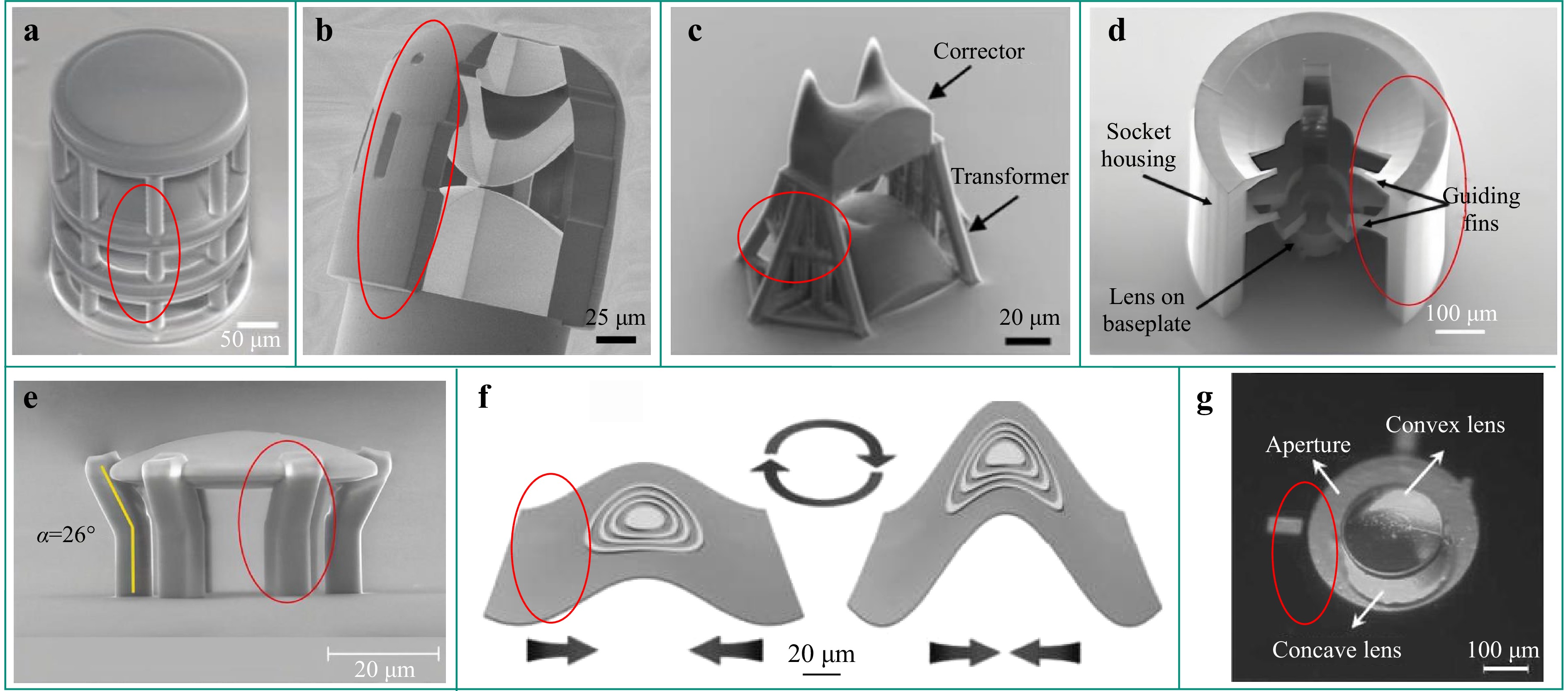
Fig. 7 a−c are the auxiliary structures for connecting multiple optical elements [obtained from ref. 204, 223, 245]. d Auxiliary structure named fiber chuck [obtained from ref. 211]. e Precompensated deformation structures [obtained from ref. 133]. f Flexible auxiliary structure [obtained from ref. 191]. g Aperture in the double-sided optical system [obtained from ref. 212].
-
Optical imaging is the most common application for optical elements. Lens systems can be constructed by combining multiple lenses to achieve more complex imaging213,214. For example, for wide-angle and large field-of-view imaging, multiple lenses with aspherical shapes are necessary to obtain superior optical performance and correct the aberrations215-217. Thiele et al. proposed a stacked imaging system with multiple integrated optical elements218. The system was manufactured in one step by TPP without requiring alignment and assembly of minimal optical elements (<200 μm in diameter and <100 μm in height). The lens system enables submicron-resolution imaging at visible wavelengths and has a field-of-view of up to 60°. The field-dependent optical aberration can be compensated for by increasing the number of refractive interfaces in the lens system. Stacked-lens systems offer excellent optical performance and are compact, at least an order of magnitude smaller than other lens systems. Galvez et al. reported the performance of three closed-focus microendoscopic distal optical systems219 (Fig. 8a). Each system used the same aperture stop placed in front of the distal optical element, and the same fiber bundle, proximal optical system, and camera. The distal optical systems they processed exceeded expectations for the working distance and angular field of view. Several microobjective lenses with different fields of view were printed on the surface of the fiber to achieve a perfect fusion of the optical fiber and objective lens.
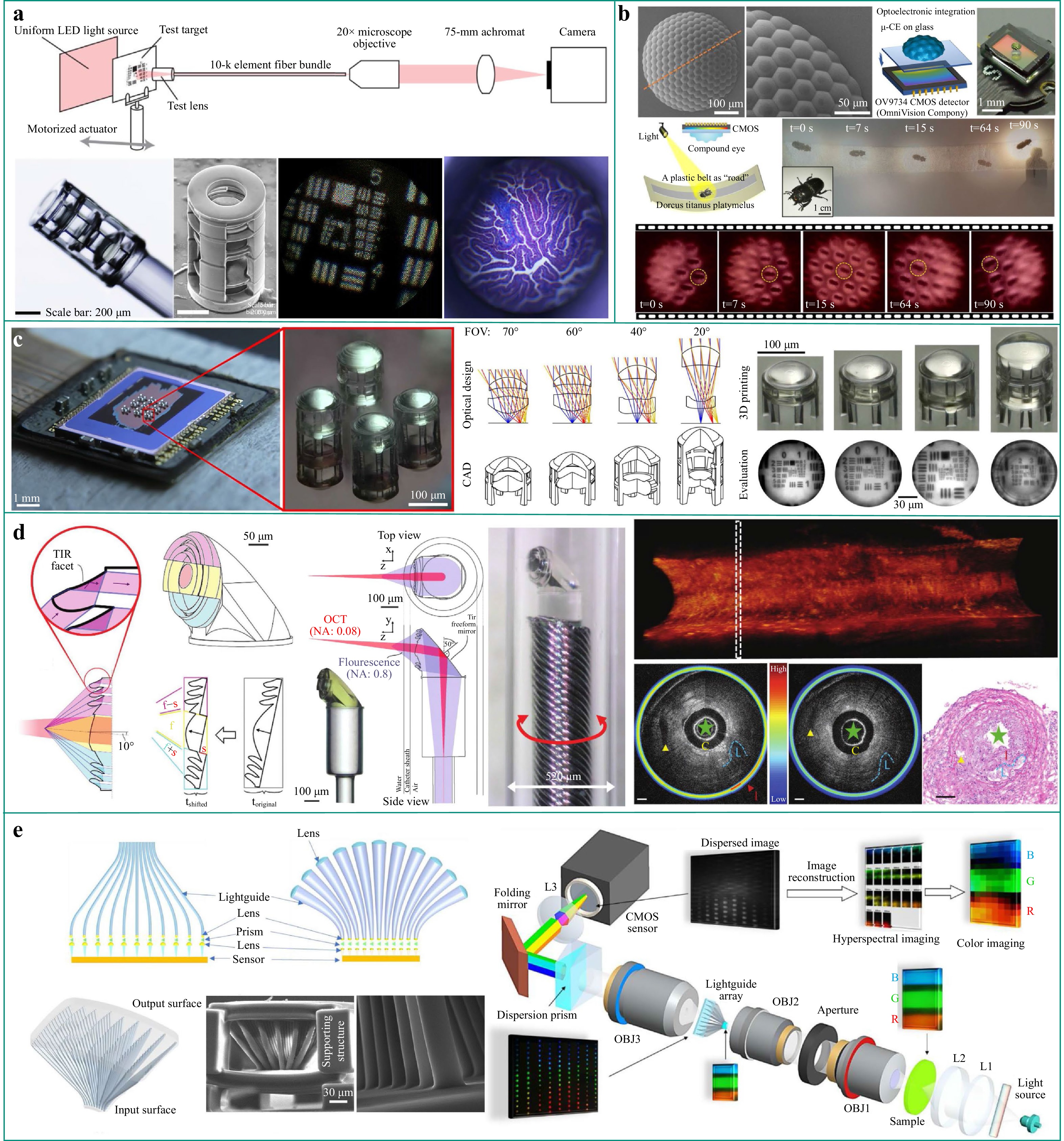
Fig. 8 a Close-focal microendoscopic on an optical fiber [obtained from ref. 219]. b Bionic Compound eyes (CE) camera with an integrated optoelectronic system [obtained from ref. 17]. c 3D-printing different multilens objectives directly onto a complementary metal-oxide semiconductor (CMOS) [obtained from ref. 215]. d Multimodal microendoscopic for fluorescence and optical coherence tomography (OCT) imaging [obtained from ref. 205]. e Lightguide system used for snapshot hyperspectral imaging [obtained from ref. 223].
Compound eyes (CE) is a natural multiaperture optical imaging system that shows significant potential in modern optics220. Hu et al. reported a bionic μ-CE camera with an integrated optoelectronic system (Fig. 8b)17. The contour of each processed eye was designed according to a logarithmic function, which can considerably increase the depth of field and focus range of small eyes. The obtained μ-CEs are integrated with a commercial complementary metal-oxide semiconductor (CMOS) detector to form a μ-CE camera, which enables large field-of-view (90°) imaging, spatial position recognition, and the trajectory monitoring of moving targets. In addition to processing optical elements directly on optical fibers, optical elements can be processed directly on the surfaces of light-emitting diodes and image sensors. Thiele et al. demonstrated a highly miniaturized camera221 that could imitate the natural vision of predators by printing different multilens systems directly on CMOS image sensors215. As shown in Fig. 8c, four lens systems with different focal lengths were combined in a 2 × 2 arrangement to achieve a 70° field of view.
Li et al. used the TPP technique to process a miniaturized endoscope directly on an optical fiber, solving conflicting issues in the design of multimode microendoscopes205, as demonstrated in Fig. 8d. This endoscope included an external lens for achieving high NA (0.8) fluorescence and an internal lens for achieving low NA (0.08) optical coherence tomography (OCT). The lens contains different but connected optical surfaces with a 330 µm diameter for fluorescence and OCT imaging. The microlens can achieve a sensitivity gain of more than 10 times, allowing for in vivo OCT and fluorescence at a lower laser power and fluorescent dye concentration, thus reducing the toxicity of the dye222.
This light-guide system can be used for snapshot hyperspectral imaging. Liang et al. developed a compact high-resolution snapshot hyperspectral imaging (HSHI) system using photoconductive arrays fabricated from a sol–gel glass material (Fig. 8e)223. Optical devices project an object onto the center of the input plane within a processed light-guide array. By arranging the output side of the light-guide array, the spectrum from each light guide can be parsed into the sensor with minimal crosstalk after passing through the collimating element, dispersing optics, and focusing element. The input and output surfaces of the light guide array can be processed into different shapes, such as concave surfaces. Concave surfaces can significantly simplify optical systems by eliminating the need to correct field curvature, which is a major complicating factor in optical design. Therefore, HSHI systems exhibit exceptional compactness and high spatial resolutions.
-
In recent years, integrating imaging microoptical elements with microfluidic chips has attracted wide attention, showing significant potential for applications in optical capture, fluidic lasers, tunable optics, etc.224-226. Lu et al. used TPP to fabricate solvent-tunable PDMS microlenses227. PDMS microlenses exhibit exceptional optical properties attributed to their high-precision and smooth surfaces, as well as their unique solvent-tunable characteristics. The focal length can be changed using different concentrations of organic solvents228. Furthermore, because of the small size of the microlens, the relatively large boundary area promotes solvent diffusion, shortening the response time required for the expansion and contraction of the lens, which can be accomplished within a few seconds. This microoptical element can be flexibly integrated into a microfluidic device, which will provide new functions to common microfluidic chips, such as optical focusing, optical imaging, and in situ monitoring.
Wu et al. integrated flexible 3D polymer micro-optical elements into the channels of microfluidic glass elements229,230, as shown in Fig. 9a. They used wet etching-assisted laser ablation to process the channels inside the glass and SU-8 to process the optical elements (2D FZPs and 3D refraction MLAs) inside the channels. The optical elements in the channel feature multicolor focusing and an enlarged focal length (greater than three times) and are capable of imaging in liquid channels. Processed optofluidic chips can achieve a success rate of up to 90% for uncoupled white blood cell counting. They designed and fabricated an optical fluidic system with two MLAs and a W filter for advanced cell filtration and counting.
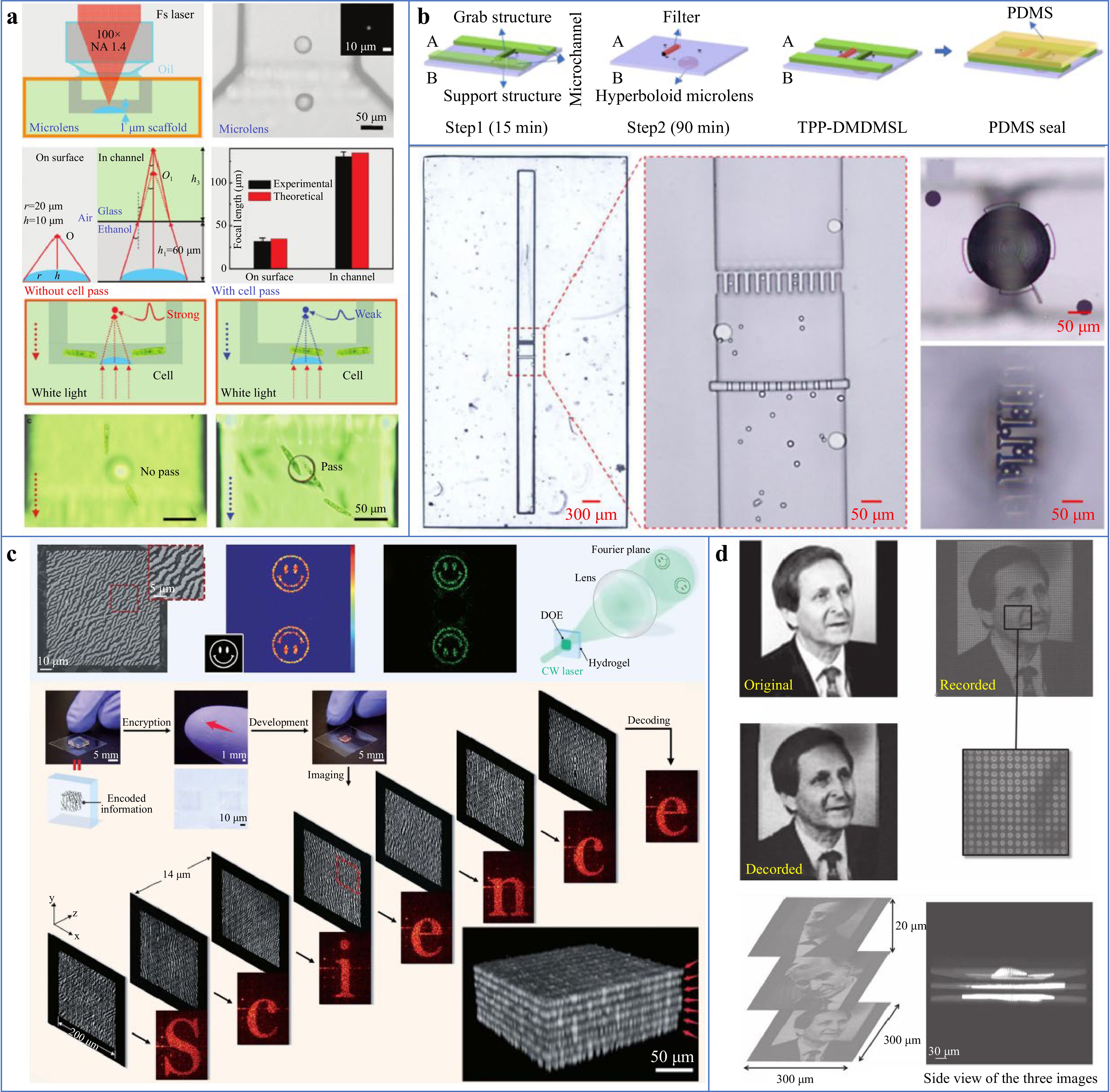
Fig. 9 a Optofluidic chip was used for uncoupled white light cell counting [obtained from ref. 229]. b Multifunctional double-sided microfluidic system [obtained from ref. 105]. c Fabrication of DOE and its applications in 3D optical storage and encryption. Fluorescent images of the decrypted holograms, in which “Science” is decoded [obtained from ref. 170]. d Pictures embedded in the glass were written with a NIR femtosecond laser and read with NUV light [obtained from ref. 231].
Based on hybrid 3D printing technology, Tan et al. designed and processed a multifunctional double-sided microfluidic system using SU-8 and PDMS material105. Fig. 9b shows a schematic of the double-sided microfluidic system, which consists of a microchannel, filtering structure, collection structure, and hyperbolic imaging lens. The microchannels and filter structures were processed using a DMD lithography system, while the hyperbolic lens and collection structures were processed using TPP. After the channel was sealed, the particles flowed into the channel with the liquid, and particles of the required size were collected after passing through the filter and collection structure. Simultaneously, the hyperbolic lens on the other side of the substrate allowed real-time observation of the collection, enabling a multifunctional microfluidic system. Experimental tests showed that the double-sided microfluidic chip offers excellent performance for the filtration of multisized particles and real-time imaging of collected particles.
-
3D imaging systems constructed using femtosecond laser processing can also be used for data storage applications231-233. By processing hydrogels using FLM, Han et al. demonstrated a method for optical storage and encryption of optically written information by physically shrinking 3D nanostructures (Fig. 9c)170. They fabricated a seven-layer structure that encodes the word ‘Science,’ with each layer containing a 200 × 200 pixel hologram. The designed holograms were patterned on a fully expanded gel using the FLM. After the complete acid-induced hydrogel shrinkage, each pixel was reduced to ~150 nm, resulting in a storage density of 20 Tb/cm3. As the feature size of a 3D structure is below the diffraction limit, only translucent rectangles lacking structural details can be observed using an optical microscope. Therefore, the processed pattern is completely invisible, and the information stored in the structure is effectively encrypted. Moreover, the contracted and desiccated hydrogels are chemically stable and endure prolonged storage. The redevelopment of these structures in a 0.5 mM aqueous NaOH solution and deposition with fluorescent materials enable the decryption of stored holograms, which can be read out by confocal microscopy.
Huang et al. used femtosecond laser ablation to store information by writing 3D patterns of perovskite quantum dots (QDs) onto glass materials234. High luminescent CsPbBr3 QDs can be reversibly fabricated or decomposed in situ by FLM or thermal annealing (350 ℃), respectively. This writing and wiping pattern can be repeated for several cycles, and the luminescent QDs are well protected by the inorganic glass substrates. Zinc phosphate glass is a femto-photoluminescent glass containing silver ions. When excited by NUV radiation, no noticeable change is observed in the refractive index; however, it exhibits notable fluorescence and nonlinear optical properties. Royon et al. demonstrated the use of a zinc phosphate glass for 3D optical recordings (Fig. 9d)231. This method provides the advantages required for 3D optical data storage, such as high storage capacity (up to hundreds of TB/cm3), high read speed (500 Mbit/s), no crosstalk, and no photobleaching of fluorescence. Furthermore, the temperature and aging tolerances of zinc phosphate glass have made it suitable for perennial storage for centuries.
-
Beam shaping generally refers to homogenizing an inhomogeneous beam (Gaussian beam, etc.) and forming it into a desired shape, such as a rectangle, hexagon, and circle235-237. Gissibl et al. fabricated phase masks directly on the end surfaces of single-mode fibers using TPP to achieve intensity shaping of the output beam238. Because the intensity-shaping phase mask was fabricated directly on the fiber core, the intensity distribution of the emitted light was highly symmetrical. Thiele et al. used IP-S to fabricate dielectric concentrators on LED chips, providing unprecedented collimation efficiency239,240 (Fig. 10a). They tested LEDs at a forward current of 10 mA and recorded the illumination distribution before and after processing the dielectric concentrator. In the collimation direction, the output light intensity increased by 6.2 times when diameters and lengths were <200 µm, and the emission half-angle decreased by 50%. This method allows for arbitrary geometries within a very small range and is suitable for miniaturizing optical elements241. An integrated single-photon source with a high optical extraction efficiency is a critical structure for applications in quantum communication242. Fischbach et al. achieved a single-photon source with excellent quantum optical properties and high extraction efficiency by directly processing a microobjective lens on a QD microlens243. Compared with structures without a microobjective, the photon-extraction efficiency improved 2.3 times. Meanwhile, excellent single-photon purity was maintained, and the required excitation power was reduced by an order of magnitude. Further optimization of the microlens/microobjective device will significantly enhance its potential as a highly efficient method for achieving fiber-coupled single-photon sources.
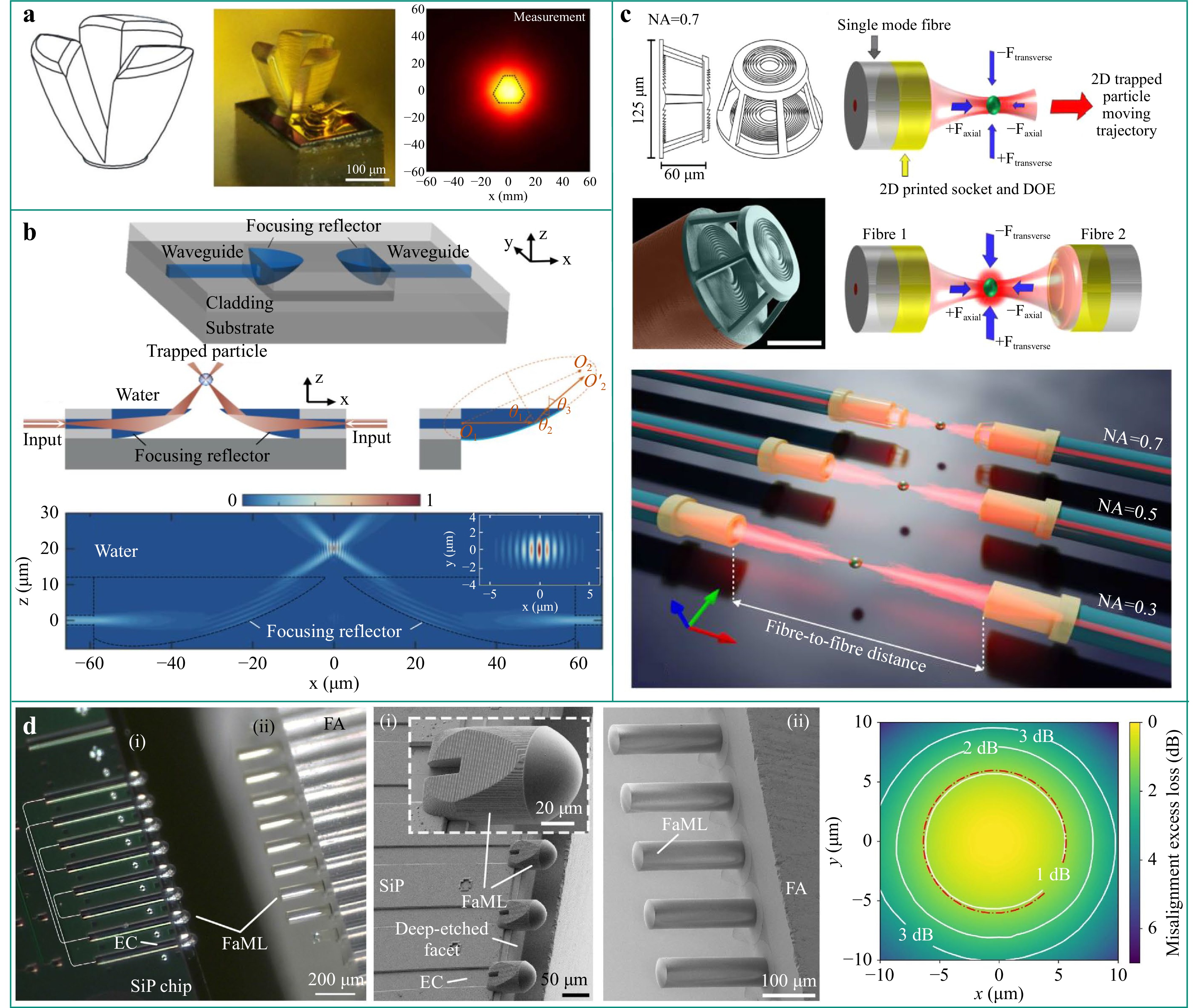
Fig. 10 a Dielectric concentrator on LED chips [obtained from ref. 239]. b On-chip optical tweezers [obtained from ref. 246]. c Efficient optical trapping technique based on reverse transmission fiber [obtained from ref. 247]. d Printing of microlenses on the surface of photonic chips and fibers to collimate and redirect beams. [obtained from ref. 248].
Optical tweezers are formed when the optical field is modulated by an optical vortex, which can be used for particle capture244. Shlomi et al. fabricated a miniature vortex mode sorter that enabled direct integration of the sorter into an optical system245. They proposed a sorter comprising two independent elements and an integrated device. These elements can handle pure vortex beams and mixed vortex beams with topological charges of |L| ≤ 3 and |L| ≤ 2, respectively. The integrated sorters were fabricated via a continuous printing process using IP-Dip. Importantly, the integrated sorter cannot be processed using other methods, such as diamond turning or computer numerical control milling.
Yu et al. demonstrated a new type of on-chip optical tweezer, which is a free-form microoptical element based on waveguide integration246. As shown in Fig. 10b, this design enables the precise positioning of the trap in the 3D region above the chip and easy adjustment of the capture potential energy. In addition, microoptical elements can be seamlessly integrated with on-chip waveguides. This allows the elements to easily access a photonic integrated circuit to endow them with new functions, such as dynamic adjustment and switching of optical traps. Furthermore, freeform reflection or refraction microoptic elements offer excellent optical efficiency (>95% efficiency from the waveguide to the focus spot) and broadband operation. A high efficiency is beneficial for reducing the capture threshold power, whereas a large spectral bandwidth facilitates the preparation of quantum states and fluorescence excitation. Finally, the real-time motion of the captured particles can be monitored by measuring the intensity of the scattered light.
Asa et al. proposed an efficient optical trapping technique based on a reverse transmission fiber that uses a converged fiber with a 3D-printed diffractive Fresnel lens on its surface247. Based on the basic principle of conventional optical trapping, increasing the NA of the focused beam changes the distribution of optical forces, leading to optical trapping in both the lateral and axial directions, as shown in Fig. 10c. Therefore, superimposition of two identical 2D trapping spots can generate a focal region. They fabricated three different Fresnel lenses on the fiber surface, which showed very stable trapping ability for dielectric particles in water. Xu et al. used TPP to fabricate microlenses to assemble advanced photonic systems248. They printed microlenses on the surfaces of photonic chips and fibers, allowing the beam to be shaped by the refractive plane, thus relaxing the axial and lateral alignment tolerances (Fig. 10d). Particularly, the emitted beam can be aligned to relatively large diameters independent of the device-specific mode field. This avoids using expensive active alignment methods and allows discrete optical elements to be placed in the free-space beam path between the photonic integrated circuits. They demonstrated the feasibility and versatility of the method through a series of demonstrations, which is an attractive path for the assembly of advanced photonic systems.
-
Various miniaturized spectrometer concepts have been demonstrated and widely used. Spectrometers are divided into three main categories: direct, computational, and filtering methods. Direct spectrometers processed by Toulouse using the TPP occupied at least two orders of magnitude less space than spectrometers processed using other methods249. Moreover, the spectral bandwidth per resolution of a direct spectrometer can be increased by one to three orders of magnitude. They theoretically evaluated the feasibility of the spectrometer in a miniature volume of 100 × 100 × 300 μm3 and demonstrated it experimentally (Fig. 11a). The resolution of the fabricated spectrometer was 9.2 ± 1.1 nm at 532 nm and 17.8 ± 1.7 nm at 633 nm. This is the first spectrometer to demonstrate a direct spatial-spectral response in this range. Hong et al. demonstrated a compact spectral imaging system using TPP250. The microspectrometer layout with dispersion elements is illustrated in Fig. 11b, comprising a lens equipped with both a grating and a dispersive prism. The dispersive spectral distribution has been accurately captured by the CMOS camera. Overall, the femtosecond laser processing microspectrometer marks an innovation in the 3D printing of microoptics.
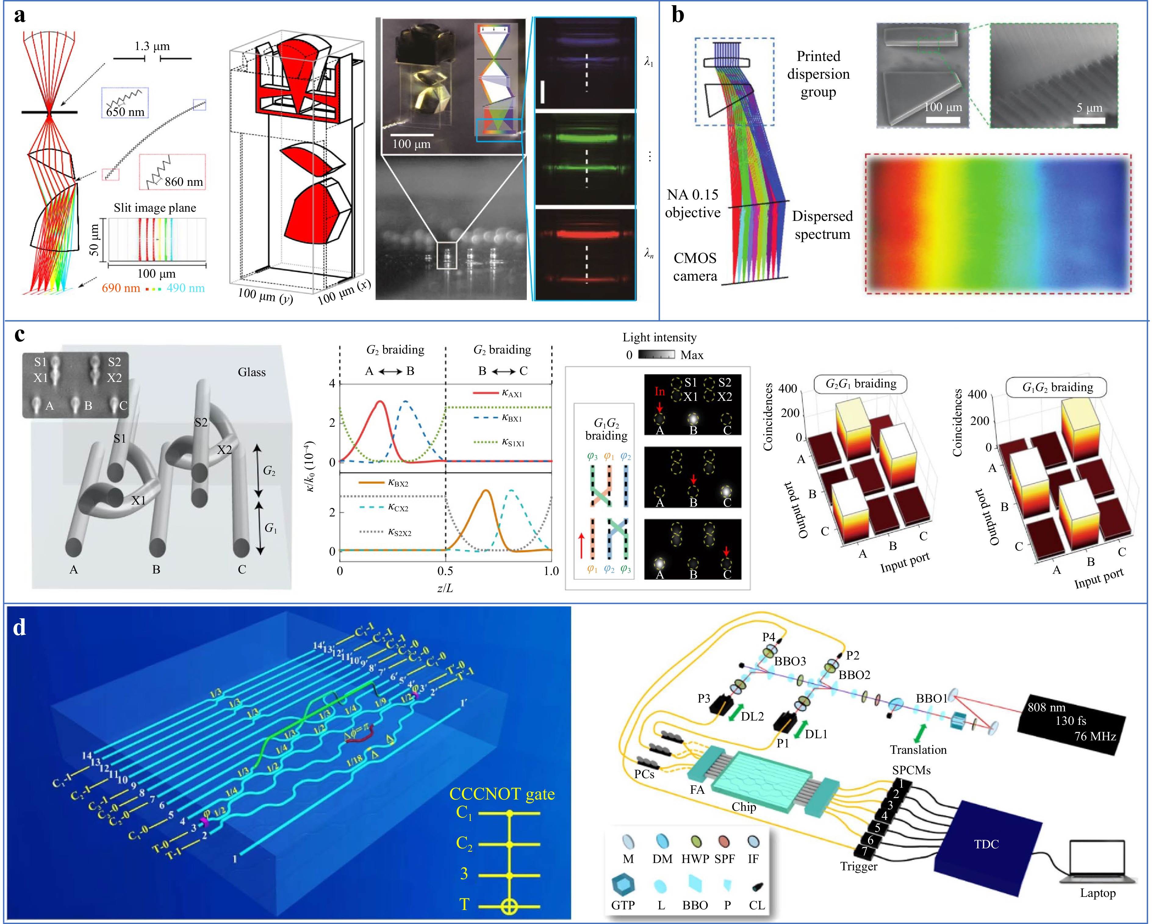
Fig. 11 a Miniature volume direct spectrometer [obtained from ref. 249]. b Micro-spectrometer with a printed dispersive assembly [obtained from ref. 250]. c Non-abelian weaving of multiple photon modes on a photon chip [obtained from ref. 252]. d On-chip path-encoded photonic quantum Toffoli gates [obtained from ref. 253].
-
Today, various physical systems aimed at general-purpose quantum computing are moving toward increasing the number of controllable qubits and enabling large-scale quantum computations. Photons have several unique advantages, such as fast traveling speed, simple single-qubit operation, long coherence time, and multiple degrees of freedom, and are suitable for quantum computing251. Zhang et al. realized the non-Abelian weaving of multiple photon modes on a photon chip252. As shown in Fig. 11c, chiral symmetry was used to ensure the degeneracy of multiple zero modes and drive them in a synchronous adiabatic evolution, thereby generating a unitary geometric phase matrix for the exchange of photon residence positions. Researchers have observed up to five modes of on-chip non-abelian weaving using both classical light and single photons. Quantum logic gates are used to construct quantum circuits in general-purpose quantum computers. Using optimized 3D structures with overpass waveguides to reduce circuit complexity, Li demonstrated on-chip path-encoded photonic quantum Toffoli gates via FLM (Fig. 11d)253. In addition, they performed path encoding of a four-quantum-controlled NOT gate to confirm the scalability of this resource-saving technique.
-
FsLDW demonstrates the ability of true 3D processing to integrate the molding of complex 3D structures and meet the processing accuracy requirements of microoptical components. Therefore, it is a crucial technology for preparing three-dimensional integrated optical systems. This paper reviews the recent developments in FsLDW-enabled imaging/nonimaging optical elements, including processing methods, processable materials, different types of optical elements, and stereoscopic systems. Various optical elements and systems based on FsLDW have been developed, enabling various cutting-edge applications. Nevertheless, FsLDW remains a novel technology, and several important development directions can be speculated.
First, the femtosecond laser processing of stereoscopic systems requires various selectable materials. Polymer resin materials have been widely processed but are commonly hindered by issues such as toxicity and poor robustness. As an alternative, glass materials with high permeability, a broad spectrum, and superior mechanical strength are highly promising for the preparation of microoptical elements254-256. Currently, the sintering temperature of the organic–inorganic hybrid liquid glass material has decreased to 650 °C, enabling the integration of optical elements with specific devices that withstand high treatment temperature257. In addition to the continuously decreasing heat-treatment temperature, various liquid glass materials are becoming more abundant, resulting in more functions. For example, the refractive index of a liquid glass can be adjusted by adding different types of nanoparticles. Glass-ceramic materials have excellent optical properties, such as high transparency, low dispersion, and a high refractive index, and can be applied to optical systems through femtosecond laser processing with further development141. Unlike single-material optical systems, multimaterial optical systems consist of optical elements fabricated using different types of materials. The combination of different materials provides advantages such as a larger refractive index range, lower dispersion, and high nonlinear effects258. In the future, femtosecond lasers are expected to process multiple materials in one system to achieve more complex functions such as a negative refractive index and metalenses.
Second, stereoscopic systems processed by FsLDW usually contain multiple optical elements and couplers connecting the optical elements, significantly increasing the processing complexity and time259,260. Therefore, the development of efficient femtosecond laser processing methods is another important development direction261-263. For example, the HVLS method can improve processing efficiency by using small voxels to process the surface of optical elements and large voxels to process the auxiliary structures between optical elements and structures inside the optical elements.
Therefore, the development of multimaterial and efficient femtosecond laser processing methods will further promote the establishment of multisystem, multidimensional, multiscale, and multifunctional stereo optical systems (Fig. 12). For example, microoptical elements can be directly processed on a fiber to form a stereoscopic integrated system to achieve functionalities such as microimaging and spectral analysis. Traditional lenses usually require a certain thickness to achieve the lens effect, whereas metalenses can achieve super-resolution imaging, ultrathin focusing, reflection elimination, super zoom, and other functions by relying on their nanoscale or submicron structures, thus forming a planar optical system with excellent performance. Moreover, photonic chips with various functions can be constructed by combining and connecting waveguides with different optical elements or detectors, such as bionic vision perception and optical communication modulator248,264,265. In general, to achieve various imaging/nonimaging functions in the extremely small spaces of miniaturized devices in the future, microoptical elements will continue to develop toward the direction of stereoscopic integration266. Further optimization and improvement of FsLDW technologies for the development of multimaterial, cross-scale, multidimensional, multiple systems, and multifunctional optical elements and systems are essential for practical and industrial applications.
-
This work was supported by the National Natural Science Foundation of China (Nos. 62275044, 62205174, 61875036), the Jinan “20 New Colleges and Universities” Innovation Team Introduction Project (202228047).
Imaging/nonimaging microoptical elements and stereoscopic systems based on femtosecond laser direct writing
- Light: Advanced Manufacturing 4, Article number: (2023)
- Received: 08 June 2023
- Revised: 26 October 2023
- Accepted: 30 October 2023 Published online: 31 October 2023
doi: https://doi.org/10.37188/lam.2023.037
Abstract: The development of modern information technology has led to significant demand for microoptical elements with complex surface profiles and nanoscale surface roughness. Therefore, various micro- and nanoprocessing techniques are used to fabricate microoptical elements and systems. Femtosecond laser direct writing (FsLDW) uses ultrafast pulses and the ultraintense instantaneous energy of a femtosecond laser for micro-nano fabrication. FsLDW exhibits various excellent properties, including nonlinear multiphoton absorption, high-precision processing beyond the diffraction limit, and the universality of processable materials, demonstrating its unique advantages and potential applications in three-dimensional (3D) micro-nano manufacturing. FsLDW has demonstrated its value in the fabrication of various microoptical systems. This study details three typical principles of FsLDW, several design considerations to improve processing performance, processable materials, imaging/nonimaging microoptical elements, and their stereoscopic systems. Finally, a summary and perspective on the future research directions for FsLDW-enabled microoptical elements and stereoscopic systems are provided.
Research Summary
Femtosecond lasers: Fabrication of imaging/nonimaging microoptical elements
Femtosecond laser direct writing (FsLDW) exhibits various excellent properties, including high-precision processing beyond the diffraction limit, and the universality of processable materials, demonstrating its unique advantages in 3D micro-nano manufacturing. Liu Hua's team from Northeast Normal University reported the development of FsLDW-enabled microoptical elements and stereoscopic systems, including three typical principles of FsLDW, several design considerations to improve processing performance, processable materials, imaging/nonimaging microoptical elements, and their stereoscopic systems. Finally, the team provided a summary and perspective on the future research directions for FsLDW-enabled microoptical elements and stereoscopic systems.
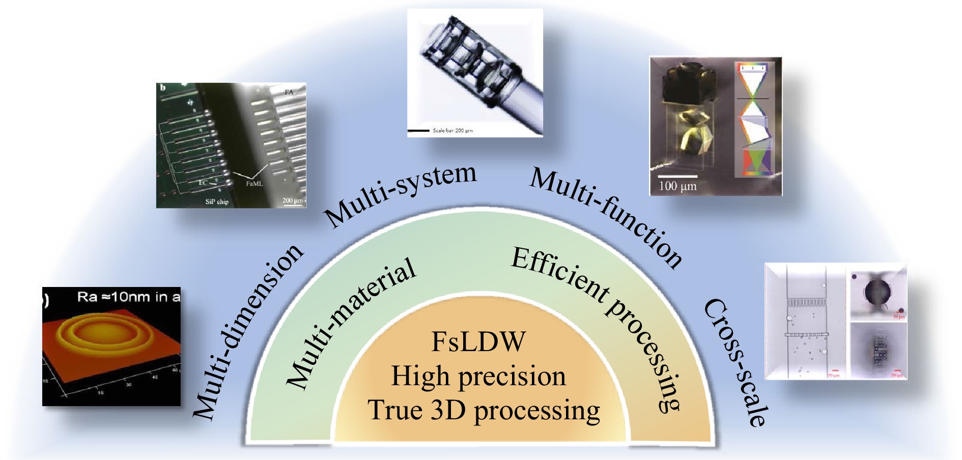
Rights and permissions
Open Access This article is licensed under a Creative Commons Attribution 4.0 International License, which permits use, sharing, adaptation, distribution and reproduction in any medium or format, as long as you give appropriate credit to the original author(s) and the source, provide a link to the Creative Commons license, and indicate if changes were made. The images or other third party material in this article are included in the article′s Creative Commons license, unless indicated otherwise in a credit line to the material. If material is not included in the article′s Creative Commons license and your intended use is not permitted by statutory regulation or exceeds the permitted use, you will need to obtain permission directly from the copyright holder. To view a copy of this license, visit http://creativecommons.org/licenses/by/4.0/.

 DownLoad: