


HTML
-
In the semiconductor industry, optical wafer metrology is a key to the manufacturing process of integrated circuits. A crucial step during fabrication is measuring the overlay, which is the lateral misalignment of a newly patterned layer with respect to the previous layer in a multilayer stacked wafer. This so-called overlay metrology is of importance for controlling the fabrication process and the early detection of problematic wafers1. To determine the overlay, dedicated metrology targets are measured using a diffraction-based overlay (DBO) technique. Here the intensity difference between $ +1^{\mathrm{st}} $ and $ -1^{\mathrm{st}} $ diffraction orders, coming from two biased overlapping gratings, scales linearly with the overlay error2−5. Currently, optical overlay metrology techniques, such as DBO, face significant challenges. First, requirements on precision approaches sub-nanometre levels5 which requires intensity level measurements in DBO with a relative precision of the order of 0.01%6. Next, the size of metrology targets is approximately 8 × 8 μm27 and these targets are placed in an environment of surrounding structures. Correctly measuring intensity levels in these small structures without suffering from optical crosstalk from surrounding structures requires imaging optics with a high numerical aperture (NA) and very low aberration levels. Finally, a wide wavelength range is desirable due to the large variety of materials that are encountered in modern chip manufacturing. Some materials are transparent at short wavelengths (≈ 400 nm) but other materials like amorphous Carbon8 only become transparent at longer wavelengths (> 1000 nm). To effectively manage these materials, an overlay metrology tool should preferably cover a very wide wavelength range from visible (VIS) to near-infrared (NIR) wavelengths. Recently, we presented off-axis dark-field digital holographic microscopy (df-DHM) as a promising new technique to address the growing challenges of overlay metrology in semiconductor industry6,9−14. DHM distinguishes itself from other microscopy techniques by digitally recording the object as a hologram via interference of the object wave with a tilted reference wave at a well-chosen angle with respect to each other. The complex object image can be derived directly from the hologram using fast Fourier transform (FFT) techniques15. The retrieved complex field gives access to amplitude and phase information which allows to correct imperfections in the imaging system16−18.
Dark-field and multi-wavelength DHM has already been described19−24 for various imaging applications like detecting sub-wavelength particles with large contrast19,20, contrast enhancement in biological imaging21, speckle-reduction23 and improved surface profiling24.
Herein, we present an off-axis df-DHM as an overlay metrology tool that can image a wide wavelength range, from VIS to NIR wavelengths. The novel aberration correction capabilities of df-DHM reported in this study offer high imaging quality over a large field of view using a relatively simple custom-made high NA imaging lens. High-NA imaging, in combination with simple optics, introduces field position-dependent or non-isoplanatic aberrations in the imaging system. In this study, we describe a fast computational correction method that allows us to correct non-isoplanatic aberrations computationally with DHM and present the experimental results over a wide wavelength range from VIS to NIR. Wafer metrology is a new field that combines digital post-processing algorithms for non-isoplanatic aberration correction with custom-made optical design approaches. In astronomy, this technique was adopted a few years ago25,26. However, in the context of astronomy the aberration corrections have been applied to incoherent systems whereas we are working with a coherent imaging system. Moreover, in astronomy, the throughput is irrelevant, whereas in the semiconductor industry, high throughput is a key indicator of a good metrology tool. In the next section, we present the processing steps and algorithms of the aberration correction method. In the Results section, we present additional experimental results obtained using aberration correction theory. Finally, we conclude by summarising our findings.
-
The resolution of an imaging system improves when the NA of lenses increases. Therefore, a high-NA lens is required to create sharp images of small overlay metrology targets. Moreover, a high NA allows us to capture diffraction orders from metrology gratings over a wide range of pitches and wavelengths, thereby enabling robust overlay metrology2,27. In this study, a 0.8-NA, two-element imaging lens was used. The drawback of a high NA in combination with only two uncoated lens elements is field position-dependent aberrations. Each object point within the field-of-view (FoV) experiences different aberrations. Such field position-dependent aberrations are also called non-isoplanatic aberrations, spatially varying blur, or 4D aberrations, wherein two dimensions are in the image plane and two dimensions are in the pupil plane28.
These non-isoplanatic aberrations can be corrected computationally because DHM retrieves the phase and amplitude information of the object via the sidebands of the Fourier transform of the hologram. These sidebands represent the interference between the object wave and the reference wave. Using computational techniques, we can easily correct field position-independent aberrations or isoplanatic aberrations, such as spherical aberrations, with a simple deconvolution, which is performed as a multiplication in the Fourier space11. Such deconvolution is computationally inexpensive. Non-isoplanatic aberrations can be corrected by applying deconvolution per object point for a given area of the considered FoV, which is computationally expensive. To make non-isoplanatic aberration correction efficient, we focused on a certain class of field-dependent aberrations that can be easily corrected via pupil distortion. This leads to a correction method based on the following three steps:
1. Isoplanatic aberration correction
2. Pupil distortion correction
3. Singular value decomposition (SVD) correction
The SVD-based method can correct all arbitrary field position-dependent aberrations. However, its computational expense scales with the extent to which aberrations vary as a function of the field position. Therefore, for speed and computational expense, it is important to first correct the aberrations as much as possible using deconvolution and pupil distortion. The aberration correction steps are described in detail in this section. Before proceeding with the correction procedure, the lens design is discussed.
-
Our imaging lens is the result of a co-optimization between an optical design and signal-processing algorithms25,26. The lens has been co-designed with as few lens elements as possible and only allows aberrations that are easy to correct computationally using the algorithms reported in this paper.
The custom-made imaging lens was manufactured by Anteryon (
www.anteryon.com ). It has an NA of 0.8 and consists of two uncoated lens elements, one of which is a plano-asphere, as shown in Fig. 1.
Fig. 1 Schematic illustration of the two-element high-NA lens.
The lens is manufactured using a replication process29,30 and is fixed in a holder on which the reference beam mirrors are integrated such that the angle between the reference and object beam is optimised (Fig. 6b). The combination of a high NA and only two lens elements yielded high field position-dependent aberrations, indicating that each field position yielded a different point spread function (PSF) in the image plane.
The lens was designed such that the aberrations correctable via pupil distortion, such as linear coma, have limited restrictions. All other field position-dependent aberrations, such as astigmatism, were minimised. This lens design allows the correction of non-isoplanatic aberration with low computational effort.
-
In general, an imaging system is characterised by its PSFs, which are images of a single point source in an object, as shown in Fig. 2a. An optical system with a perfect imaging lens results in an ideal spherical wavefront and a diffraction-limited PSF, i.e. an Airy Disk, as shown in Fig. 2b. However, a non-ideal lens deforms the wavefront, resulting in an aberrated PSF, as shown Fig. 2c.

Fig. 2 Imaging system characterized by its point-spread function (PSF). a Schematic representation of a point scatterer illuminating the imaging lens with spherical waves. b An aberration free imaging lens results in an ideal spherical wavefront and a diffraction-limited PSF in the image plane. c A non-ideal lens deforms the wavefront resulting in an aberrated PSF presented for the case of spherical aberrations.
The mathematical relation between the object field $ o(\vec{H}) $ and the image field $ i(\vec{H}) $ is given by
$$ \begin{array}{*{20}{l}} i(\vec{H}) = FT^{-1}\left[ \tilde{A} (\vec{\rho}) \int e^{i \tilde{W}(\vec{\rho},\vec{H})} e^{i \vec{\rho} \cdot \vec{H}} o(\vec{H}) d\vec{H}\right], \end{array} $$ (1) where $ FT $ denotes a 2D Fourier Transform, $ \vec{H} $ denotes the coordinate vector in the object plane, $ \vec{\rho} $ is the vector in Fourier space of the exit pupil plane, $ \tilde{A} $ is the aperture function, $ \tilde{W} $ is the non-isoplanatic aberration function and ~ denotes a function in pupil space. The non-isoplanatic aberration function $ \tilde{W} $ from Eq. 1 can be described with three terms,
$$ \begin{array}{*{20}{l}} \tilde{W}(\vec{\rho},\vec{H}) = \tilde{W}_{iso}(\vec{\rho})+ \tilde{f}(\vec{\rho}) \, \vec{H}\cdot\vec{\rho} + \delta \tilde{W} (\vec{\rho},\vec{H}). \end{array} $$ (2) Each term of Eq. 2 is corrected in one of the three aberration correction steps. The first term is corrected in the isoplanatic aberration correction step. The pupil distortion correction step corrects the second term of Eq. 2. Finally, during the SVD correction, the third aberration term, which comprises all the remaining aberrations given by $ \delta \tilde{W} $, will be corrected.
-
In the case of isoplanatic aberrations, the PSF deformation is constant over the FoV, i.e. field position-independent. Previously, we demonstrated the computational correction of isoplanatic aberrations via a single deconvolution of one PSF in the context of overlay metrology, as this was allowed for the lower NA lens used at a substantially smaller wavelength range11. In this method, a nano-sized point scatterer is imaged in the centre of the FoV, resulting in the retrieval of the wavefront aberration of the imaging lens. As the first correction step, deconvolution is applied to a measured image field by multiplying the field with the conjugate wavefront aberration in the Fourier space for a PSF, preferably selected at a location in the FoV close to the nodal point. The nodal point is the point of the optical system for which an incoming ray leaves the system with the same direction. For a curved surface, such as the imaging lens, the nodal point is located at the centre of the curvature of the surface.
For the correction of the isoplanatic aberration, the aberrated complex-valued image field $ i(\vec{H}) $ is retrieved from the camera in real space given by
$$ \begin{array}{*{20}{l}} i(\vec{H}) = h(\vec{H}) * o(\vec{H}), \end{array} $$ (3) where $ h(\vec{H}) $ represents the selected 2D PSF close to the nodal point in field space. By performing a 2D Fourier transform, we back-propagate the aberrated image field to the exit pupil in pupil space given by
$$ \begin{array}{*{20}{l}} \tilde{i}(\vec{\rho}) = \tilde{h}(\vec{\rho})\cdot\tilde{o}(\vec{\rho}). \end{array} $$ (4) In pupil space, a deconvolution multiplication is performed on the aberrated image field $ \tilde{i}(\vec{\rho}) $ with the complex conjugate of the retrieved transfer function $ \tilde{h}(\vec{\rho})^* $ to correct for the isoplanatic part $ \tilde{W}_{iso} $ of the aberration function in Eq. 2. This results in the following Wiener deconvolution, yielding the isoplanatic-aberration corrected object field in pupil space
$$ \tilde{o}_{c1}(\vec{\rho}) = \frac{\tilde{h}(\vec{\rho})^*}{|\tilde{h}(\vec{\rho})|^2 + \epsilon} \cdot\tilde{i}(\vec{\rho}), $$ (5) where $ \epsilon $ is a non-zero positive value that mitigates the amplification of noise. Performing an inverse Fourier transform results in the isoplanatic-aberration corrected object field in field space, given by $ o_{c1}(\vec{H}) $. In the following part, the remaining non-isoplanatic correction steps will be explained.
-
As mentioned previously, non-isoplanatic aberrations can be corrected by applying deconvolution per object point. This method is computationally expensive because the computational expense scales with the degree of nonisoplanatism. This is not the case for pupil distortion. Pupil distortion represents non-isoplanatic aberrations that can be efficiently computationally corrected via coordinate remapping.
As shown in Fig. 3, we computationally correct the pupil distortion by remapping the coordinates of the aberrated pupil plane. First, the isoplanatic corrected object field in field space $ o_{c1}(\vec{H}) $ is moved to the pupil field by Fourier transform, resulting in $ \tilde{o}_{c1}(\vec{\rho}) $. Then, in pupil space, the distortion is corrected by remapping the coordinates $ \vec{\rho} $ of the distorted pupil field $ e^{i f (\vec{\rho})\vec{H} \cdot \vec{\rho}} $ to the coordinates $ \vec{\rho}' $ of the undistorted pupil field, where $ f (\vec{\rho}) $ represents the distortion strength. This distortion correction method can be shown in detail using coma aberrations as an example of pupil distortion. The wavefront deformation for low-order coma ($ W_{131} $) is absent at the nodal point close to the centre of the FoV, and increases linearly with the field coordinate $ \vec{H} $ inside the FoV according to28,
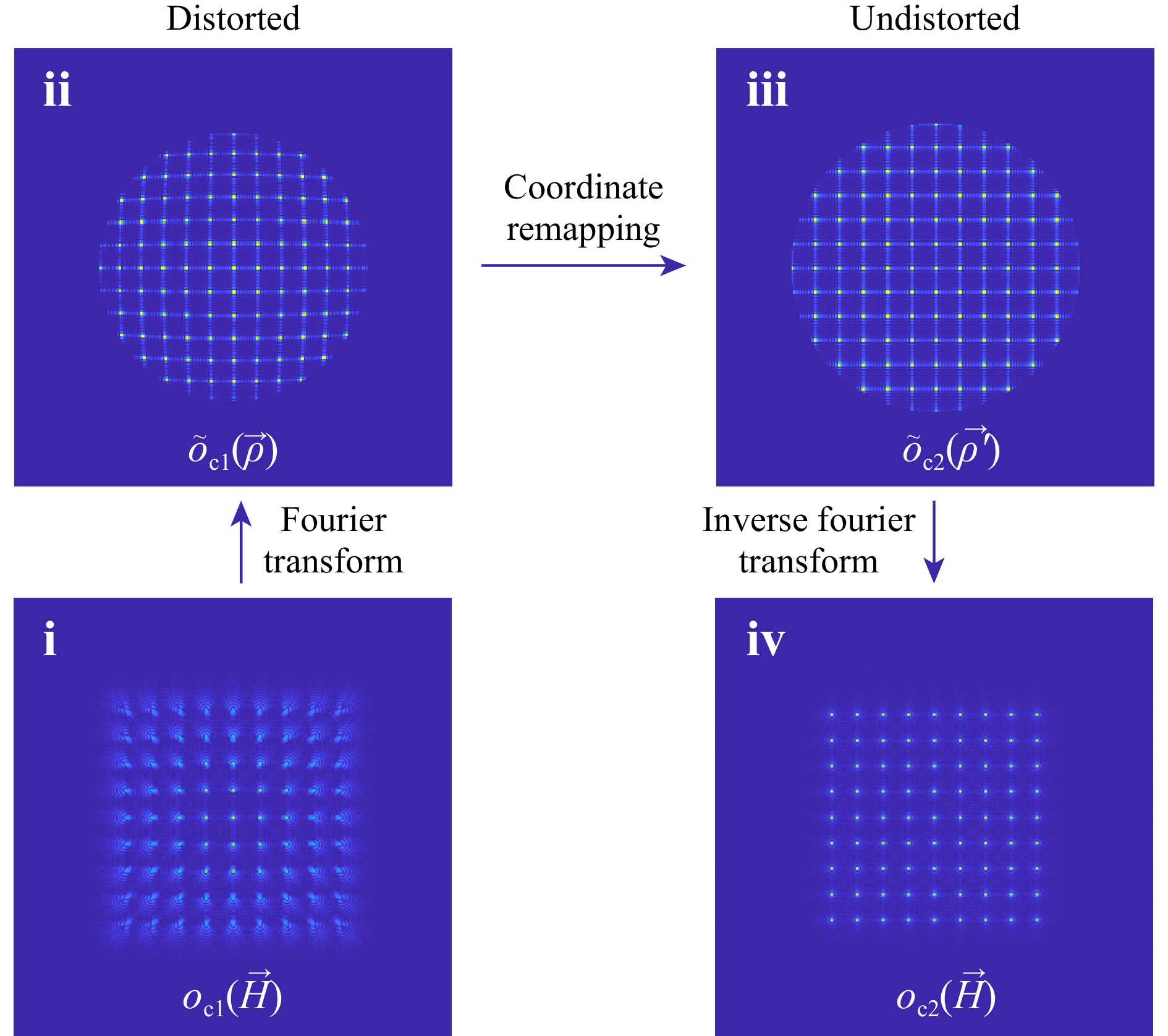
Fig. 3 Simulated pupil distortion correction approach with the corresponding fields where (i)-(iv) indicates the sequential order of steps taken during the pupil distortion correction. (i) aberrated amplitude image simulated nano-hole test grid with arbitrary dimensions. (ii) Fourier transform of distorted image plane (i). (iii) Pupil plane after remapping of the pupil plane coordinates. (iv) Retrieved undistorded amplitude of the simulated test grid after pupil distortion correction.
$$ \begin{array}{*{20}{l}} f(\vec{\rho}) = W_{131} (\vec{\rho} \cdot \vec{\rho}). \end{array} $$ (6) In combination with the phase of the regular factor in the Fourier transform relation given by $ (\vec{H}\cdot\vec{\rho}) $, one can rewrite Eq. 6 as,
$$ \begin{array}{*{20}{l}} (\vec{H}\cdot\vec{\rho}) + f(\vec{\rho})(\vec{H}\cdot\vec{\rho}) = (\vec{H}\cdot\vec{\rho})(1+W_{131}\vec{\rho^2} ). \end{array} $$ (7) After the correction, the coordinates correspond to the undistorted coordinates $ \vec{\rho'} $ given by,
$$ \begin{array}{*{20}{l}} (\vec{H}\cdot\vec{\rho})(1+W_{131}\vec{\rho^2} ) \Rightarrow (\vec{H}\cdot\vec{\rho'}). \end{array} $$ (8) Therefore, the pupil coordinate remapping for only coma aberration $ W_{131} $ is given by
$$ \begin{array}{*{20}{l}} \vec{\rho}(1+W_{131}\vec{\rho^2} ) \Rightarrow \vec{\rho'}, \end{array} $$ (9) where the factor $ W_{131} $ defines the distortion strength. This pupil coordinates remapping results in a distortion-corrected object field in pupil space given by $ \tilde{o}_{c2}(\vec{\rho}') $. Then, performing an inverse Fourier transform results in the isoplanatic aberration and distortion-corrected intermediate object field in field space, given by $ o_{c2}(\vec{H}) $. This method is computationally efficient since it only contains two simple Fourier Transforms independent of the amount of pupil distortion.
-
Next, to correct for remaining small residual aberrations, a more general correction method based on SVD is applied. The non-isoplanatic aberrated image, Eq. 10, can be described as a linear system with a 4D-PSF matrix denoted $ H_{4\mathrm{D}} $ between the object $ o $ and the image $ i $,
$$ \begin{array}{*{20}{l}} i = H_{4\mathrm{D}} \cdot o. \end{array} $$ (10) Since direct inversion is computationally very inefficient due to the large size of $ H_{4\mathrm{D}} $, we assume that in a small region around a certain image point the PSF is approximately constant. This way, we can locally correct the image by applying a deconvolution with the PSF at that point. In order to apply $ H_{4\mathrm{D}} $ and its inverse in a computationally efficient manner, we introduce an SVD-based deconvolution. The local deconvolution kernels for the 2D-PSFs, which remain after the first two correction steps, for all object points are reshaped into 1D columns, and are put in the transfer matrix $ C $ which has the following SVD-decomposition
$$ \begin{array}{*{20}{l}} C = U \cdot S \cdot V^T, \end{array} $$ (11) where $ U $ is a matrix with its columns comprising the modal isoplanatic 2D-deconvolution kernels denoted by $ U = d_k(\vec{H}) $, where $ k $ denotes the column index of matrix $ U $. The second part of Eq. 11 is a 2D matrix describing the 2D modal weight factors, which represents the non-isoplanatism, $ S \cdot V^T = w_k(\vec{H}) $, where $ k $ represents the row index of matrix $ SV^T $. The aberration-corrected object-field is now obtained by performing the SVD-based deconvolution for 4D aberrations given by
$$ o_{c3}(\vec{H}) = \sum\limits_{k=1}^{k_{max}} d_k(\vec{H}) * [w_k(\vec{H})\cdot o_{c2}(\vec{H})], $$ (12) where $ k_{max} $ denotes the number of used SVD-modes. By applying this SVD-theory one could describe each PSF in the FoV as a sum of PSF modes with a corresponding weight factor, as shown in a simulated example in Fig. 4b. The singular value represents the contribution of a certain PSF mode to the measured PSFs in the FoV, as illustrated in Fig. 4c. The computational load of the SVD increases with the number of PSF modes defined as $ k_{max} $ and equals $ (k_{max}+1) $ times a 2D-FFT. In this study, the singular value as function of mode number $ k $ decays exponentially, as shown in Fig. 4d. Therefore, a value of 10 is chosen for $ k_{max} $. The overall aberration correction theory is translated into an algorithm, and the flowchart is presented in Fig. 4a. The algorithm is split into a calibration part and a correction part, which will be discussed in the Experimental results section.

Fig. 4 Supporting algorithm diagrams a Algorithm flowchart of non-isoplanatic aberration calibration and correction. b Simulated example of PSF modes and their corresponding weights. c Diagram of the singular value as function of mode number $ k $ from b. d Experimentally obtained singular values as function of the mode number $ k $ with $ k_{max} $ = 10 indicated with the red line.
-
Off-axis df-DHM is a coherence imaging system in which the diffracted field from an object interferes with a tilted reference field resulting in an interference pattern at the image sensor called a digital hologram15. In our df-DHM concept, for the application of overlay metrology, both the $ +1^{\mathrm{st}} $ and $ -1^{\mathrm{st}} $ diffraction orders are measured simultaneously by illuminating an overlapping grating pair under an oblique angle and interfering the diffracted fields with their corresponding off-axis reference fields (Fig. 5a). The resulting digital hologram intensity pattern consists of two overlapping interference patterns (Fig. 5b). Using a 2D FFT, we computationally propagate from the image plane to the pupil plane and obtain an angular spectrum with a baseband and four sidebands. The baseband is always placed at the centre of the Fourier transform of the hologram and does not contain any information about the phase of the object or angle of the reference wave. The sidebands encode all sample information, both in amplitude and phase. Due to a well-chosen off-axis configuration of the reference beam, the $ +1^{\mathrm{st}} $ and $ -1^{\mathrm{st}} $ diffraction order sidebands and their complex conjugates are fully-separated from the baseband (Fig. 5c)6,31. One of the sidebands is spatially filtered using a circular numerical filter which matches with the exit pupil of the objective lens and translated to the centre of the pupil plane (Fig. 5d). Finally, an inverse FFT is performed on the translated sideband, which retrieves the object fields of either the $ +1^{\mathrm{st}} $ and $ -1^{\mathrm{st}} $ diffraction orders depending on the selected sideband. The absolute value of the complex object field provides the amplitude information, and the argument of the reconstructed field provides the phase information (Fig. 5e). The retrieved amplitudes of the $ +1^{\mathrm{st}} $ and $ -1^{\mathrm{st}} $ diffraction order images, schematically illustrated in the retrieved amplitude of Fig. 5e, can be used for DBO metrology on dedicated metrology targets that consist of overlapping biased gratings as shown in Fig. 8. Further details on DBO and these overlapping gratings are provided in2,6,27.

Fig. 5 Schematic illustration of off-axis holographic recording and processing concept. a Schematics of the dark-field off-axis digital holography microscopy concept. b Recorded digital hologram with two overlapping interference patterns of the $ +1^{\mathrm{st}} $ and $ -1^{\mathrm{st}} $ diffraction orders. c The angular spectrum of the digital hologram retrieved by performing an 2D-FFT back-propagating to the pupil plane. d Selecting the sidebands and translating them to the centre of the pupil plane. e Reconstructed object fields via inverse FFT of the selected sideband, resulting in the retrieval of the object amplitude and phase information.
-
The experimental data presented in this study were obtained using a breadboard setup of the df-DHM concept. A schematic representation of the setup is given in Fig. 6, similar to the setup described in Ref. 6. The df-DHM consists of a fibre-coupled supercontinuum white light source (Leukos Rock 400) combined with a dichroic mirror with a 950-nm cutoff wavelength to split the wavelength range into two different parts. One covers the VIS regime, and the second covers the NIR wavelength range, as indicated in Fig. 6a in green and red, respectively. First, the broadband output from the supercontinuum source is spectrally filtered by an acousto-optic tunable filter (AOTF) with a bandwidth $ \Delta \lambda $ in the range of 4 nm to 8 nm and covers the VIS wavelength range of 400 - 700 nm. For the longer wavelengths in the NIR regime, a filter wheel containing interference filters is used. The filters cover 1064 nm and a range of 1100 - 1600 nm in steps of 100 nm with a bandwidth varying from 10 nm to 12 nm. After tuning the wavelength, the beam intensity is split using a 90:10 beamsplitter for the VIS regime and a 70:30 beamsplitter for the NIR regime, to create an illumination and reference beam respectively. Thereafter, a non-polarizing 50:50 beamsplitter is used in both paths for parallel acquisition of the $ +1^{\mathrm{st}} $ and $ -1^{\mathrm{st}} $ diffraction orders. The coherence length is of the order of 100 μm, hence the optical path length difference between the $ +1^{\mathrm{st}} $ and $ -1^{\mathrm{st}} $ illumination paths is set much longer than the coherence length (a few centimetres), so that there is no interference between them.

Fig. 6 A schematic representation of the experimental setup. a The beamsplitter part of the setup consists of two parallel beam paths. The supercontinuum source is split via a dichroic mirror with a cut-off wavelength of 950 nm in two beams. One for the visible (VIS) regime (400-700 nm), where the wavelength is tuned using an AOTF and the other beam for the near-infrared (NIR) (1064-1600 nm) tuning the wavelength with an interference filter. Each beam is split into a reference and illumination beam using a 90:10 and 70:30 beamsplitter for the VIS and NIR regime respectively. Afterward, 50:50 beamsplitters split the beam into two illumination and two reference beams. The two reference beam fibers are placed on a translation stage to create two delay lines. The beams are guided via polarization maintaining single mode fibres to the sensor head. b The illumination beams coming from the fibres are collimated by an objective and are diffracted on the sample under an angle of 70°. The imaging lens captures both the $ +1^{\mathrm{st}} $ and $ -1^{\mathrm{st}} $ diffraction orders. Each diverging reference beams is redirected via a mirror to the image sensor.
The beams are then coupled into polarizing-maintaining single mode (PM-SM) fibres to transmit light from the beamsplitter part in Fig. 6a to the sensor head, as shown Fig. 6b. The in-coupling sides of the reference fibers are placed on translation stages to act as a delay line to match the path difference between every object and reference beam pair. In the sensor head (Fig. 6b) the output of the SM illumination fibres is focused using a pair of lenses and redirected using a silver mirror to illuminate the target from opposite directions at an incident angle of approximately 70° with respect to the normal plane of the sample. Light diffracted from the sample is then captured by the custom made Anteryon lens (NA = 0.8 and design wavelength 650 nm) and imaged on the camera. The reference fiber outputs do not have collimating optics; therefore, the diverging beams from the fibre tips propagate in free space to the image sensor after being reflected from the two built-in mirrors on the lens holder, as shown in Fig. 6b. At the camera level, the diffracted beams interfere coherently with their corresponding reference beams, resulting in a digital hologram. The camera used for the VIS regime is the Basler acA4112-8gm with a 12 Mpixel CMOS image sensor and 3.45 μm pixel size. For the NIR regime the camera Aval ABA-013VIR-GE with Sony IMX990 sensor is used, with a pixel size of 5 μm.
-
In this section, we present an experimental demonstration of the non-isoplanatic lens aberration calibration and correction. First, the calibration procedure of the 4D PSFs with a specific calibration sample and the corresponding results are presented. Next, we present the non-isoplanatic aberration correction for dedicated overlay target images.
-
Calibration of the field position-dependent aberrations is required to perform the non-isoplanatic aberration correction described in the Theory section. The calibration sample consists of a 2D grid of nanoholes. The nanoholes were fabricated on a Si wafer with a SiN etching layer using E-beam lithography. Each nanohole, having a cylindrical shape with a diameter and depth of 100 nm, acts as a point scatterer by diffracting spherical waves. During calibration, the complex-valued image field of a nanohole grid is measured to determine the local PSF and thereby the aberrations at different object-field positions. Thus, the nanoholes probe the spatial variation of the 4D aberrations via multiple local PSFs. An example of a measured 70 × 70 μm calibration grid with a pitch of 7 μm is given in Fig. 7a. This calibration grid is measured using a wavelength of 532 nm.

Fig. 7 Retrieved amplitude of a measured nanohole-calibration grid. a 70 × 70 μm nano-hole calibration grid with a pitch of 7 μm at a measurement wavelength of 532 nm. b Magnified image of inset (i) where the PSF has high field position-dependent aberration levels. c Magnified image of inset (ii) where the PSF mainly suffers from isoplanatic aberrations.
From the measured field position-dependent PSFs presented in Fig. 7, it is clear that the aberrations contain a high amount of linear coma that increases towards the edges of the FoV, as indicated by the enlarged section in Fig. 7b. The tails of the PSFs point towards the nodal point of the optical system, shown in Fig. 7c. In our approach, there is a close cross-link between the correction and calibration of the aberrations. Because the calibration data and the target data follow the same processing steps, any uncertainty in the calibration grid centred at the nodal point is resolved. The center of the calibration grid therefore only needs to be roughly at the position of the nodal point.
-
The calibration measurement presented in the previous section is used to perform computational correction following the three correction steps described in the Theory section. The purpose of the df-DHM setup is to measure overlay on dedicated overlay targets with different pitches. A test wafer with dedicated targets is used to verify the performance of the proposed correction approach. Each target consists of four overlapping grating pairs, as shown in Fig. 8. The gratings in the bottom layer are etched in Si with an etch depth of 90 nm. The top layer gratings are lithographically made in a resist layer with a thickness of 90 nm. The square overlapping gratings have a size of either 5 μm, 8 μm or 10 μm and have a programmed overlay bias d of 20 nm.

Fig. 8 Schematic illustration of a dedicated overlay target with biased gratings.
A raw amplitude image of these overlay targets, retrieved from a single measured hologram without applying any lens aberration correction, is shown in Fig. 9a. In this image, overlay targets with sizes of 10 μm, 16 μm and 20 μm and varying pitches in the range of 400 nm to 900 nm are shown.

Fig. 9 Experimental results of the aberration correction method for the VIS wavelength regime. a Retrieved amplitude image from a measured hologram of biased overlay gratings with sizes of 10 μm, 16 μm and 20 μm and varying pitches in the range of 400 nm to 900 nm. No lens-aberration correction has been applied to this image. The measurement has been performed at wavelength of $ \lambda $ = 532 nm and a bandwidth $ \Delta \lambda $ = 1 nm over a FoV of 140 × 100 μm2. b Field-position-dependent aberration corrected retrieved amplitude image from a measured hologram of biased overlay gratings. c Magnified image of the aberrated 400 nm pitch targets, inset (i) and magnified image of the aberration corrected 400 nm pitch targets, inset (ii). d Cross sections of the aberrated targets c (i), aberration corrected targets c (ii) and simulated targets without any aberrations.
Fig. 9 is measured at a wavelength of $ \lambda $ = 532 nm and a bandwidth $ \Delta \lambda $ = 1 nm. The aberrations are relatively low in the centre of the FoV. The 4D aberrations increase as one moves further towards the edges of the FoV. In particular, the small 10 × 10 μm2 sized overlay targets are significantly affected by the field position-dependent lens aberrations. After correcting the field position-dependent aberrations we obtain the retrieved amplitude images presented in Fig. 9b. Notably, for the overlay targets with a large pitch (pitch: 700,800, and 900 nm) relative to the measurement wavelength of 532 nm, the second diffraction order is captured by the imaging lens as well. This results in an interference pattern between the first and second diffraction orders on top of the homogeneous amplitude distribution of the first diffraction order. Fig. 9d shows the vertical cross-sections of magnified insets (i) and (ii) of Fig. 9c. By comparing the uncorrected normalised amplitude (black) and aberration-corrected normalised amplitude (red) with the unaberrated simulated normalised amplitude (blue), it can be concluded that the aberration correction defines the target area more as a homogeneous square amplitude. Nevertheless, after aberration correction, there is still a deviation left with respect to the unaberrated simulated targets. The root cause of the residual error is discussed in the following section.
-
As presented in the previous section, residual aberrations remained after applying the aberration correction scheme. The wavefront error primarily results in the broadening of the PSF, which reduces its peak intensity. The quality of optical image formation can be properly quantified using the Strehl ratio S, originally introduced in astronomy by Karl Strehl32. The Strehl ratio is defined as the ratio of the peak intensity in the aberrated PSF to the peak intensity of a diffraction limited PSF33
$$ S = \frac{I_{PS F \text{, measured}}}{I_{PS F \text{, diffraction-limited}}}, $$ (13) where $ I_{PSF} $ is the maximum intensity of the PSF. A perfectly unaberrated optical system results in a Strehl ratio of 1.
To calculate the Strehl ratio of our df-DHM setup, we performed aberration correction on the nanohole calibration grid, as shown in Fig. 10.

Fig. 10 Non-isoplanatic aberration corrected PSF amplitude images measured at a wavelength of 532 nm compared to a simulated diffraction limited PSF. a Uncorrected amplitude image of nanohole calibration grid over the entire FoV. b Magnified amplitude image of inset (i) from a. The columns from left to right decreases the aberration levels via the earlier described correction steps and their corresponding cross sections through the peak intensity (1-4). Compared to the simulated diffraction limited PSF (5).
Fig. 10a shows the uncorrected amplitude image of the nanohole calibration grid measured at a wavelength of 532 nm. We calculated the Strehl ratio of a PSF which suffers from field position-dependent aberration, as indicated by (i). A magnified image of this PSF after each correction step and its corresponding cross-section are presented in Fig. 10b (1-4). Fig. 10b (5) shows the simulated diffraction limited PSF. The calculated corresponding Strehl ratios after each aberration correction step are listed in Table 1.
Processing step Strehl ratio Uncorrected 0.094 Isoplanatic correction 0.169 Pupil distortion correction 0.792 SVD correction 0.810 Table 1. Strehl ratio after each aberration correction step
After a full aberration correction procedure the Strehl ratio equals $ S $ = 0.810. The difference with a perfect Strehl ratio of 1 can be explained according to the following limitations of the aberration correction method:
1. Sample surface roughness: The SVD step mainly suffers from sample surface roughness. The roughness of the sample surface adds noise to the SVD method because the PSFs are measured on a calibration grid sample.
2. Lens surface roughness: Similar to the sample surface roughness, the lens surface roughness also adds noise to the aberration correction, resulting in an image that is not perfectly corrected.
3. PSF cropping: Sample surface and lens roughness broadens the PSF significantly. During the SVD correction step, every PSF is cropped around a certain radius. Cropping, in combination with roughness, introduces errors by truncating the PSF.
4. Maximum SVD modes: The number of used SVD modes to describe the field position-dependent PSFs involves a tradeoff between processing time and accuracy. Therefore, limiting the number of SVD modes used contributes to the overall residual aberrations.
Even though the above-mentioned limitations contribute to a residual aberration in the aberration corrected image, a Strehl ratio $ S \geq $ 0.8 generally corresponds to the diffraction-limited performance of the imaging system34.
-
Continuous developments in the semiconductor industry have led to the use of new materials that are almost opaque at VIS wavelengths and become more transparent at NIR wavelengths. One example is Ruthenium in the direct metal etch-processing steps35. However, our df-DHM concept can image NIR wavelengths; here, we demonstrate the aberration correction capabilities at a NIR wavelength. In Fig. 11, we present an aberration correction measurement on overlay targets using a wavelength of 1300 nm. Fig. 11a shows the retrieved amplitude from a hologram measured at a wavelength of $ \lambda $ = 1300 nm with a bandwidth of $ \Delta\lambda $ = 12 nm. The pitch of the upper two overlay targets is 900 nm and that in the bottom three targets is 760 nm. Moreover, there is a small dust particle visible underneath the top right overlay target. It is important to note the FoV of the NIR camera with the Sony IMX990 sensor is 4.5 times smaller than the FoV of the VIS camera with the 12 Mpixel CMOS image sensor. As a result, the field position-dependent aberrations in the NIR measurements are less significant at the edges of the FoV compared to the VIS measurements. Fig. 11b shows the field position-dependent aberration-corrected retrieved amplitude. In particular, the highly aberrated overlay targets with a pitch of 760 nm (bottom row), of which the $ 1^{\mathrm{st}} $ diffraction order goes through the edge of image lens pupil, improve significantly after correction. Finally, in Fig. 11c, the cross section (i) and (ii) are compared to a simulated target without any aberrations. The cross sections show a significant improvement after aberration correction.

Fig. 11 Experimental results of the aberration correction for the NIR wavelength regime. a A retrieved amplitude image of biased overlay targets with sizes of 10 $ \mu $m, 16 $ \mu $m and 20 $ \mu $m and varying pitches of 900 nm (top two targets) and 760 nm (bottom three targets). No lens-aberration correction has been applied to this image. b A field-position-dependent aberration corrected retrieved amplitude image of the same biased overlay targets. The measurement has been performed with a wavelength of $ \lambda $ = 1300 nm and a bandwidth $ \Delta \lambda $ = 12 nm. c Cross sections of the aberrated targets b (i), aberration corrected targets b (ii) and simulated targets without any aberrations.
In this study, the experimental results at a measurement wavelength of 532 nm and 1300 nm are presented in detail. To demonstrate that this aberration correction method also has good performance between the two wavelengths, aberration correction was performed at wavelengths of 632 nm and 1064 nm. This results in the four Strehl ratios presented in Table 2, calculated for the PSFs at the edge of the FoV.
Wavelength (nm) Strehl ratio 532 0.810 632 0.852 1064 0.756 1300 0.732 Table 2. Calculated Strehl ratio for different measurement wavelengths
The highest Strehl ratio is achieved at a wavelength of 632 nm, which is closest to the objective design wavelength of 650 nm.
-
In conclusion, we demonstrated that in our df-DHM concept, where we retrieve the full complex field, we are able to correct the non-isoplanatic lens aberrations in a computationally efficient manner through the co-design of a dedicated imaging lens and a three-step algorithmic approach.
We first presented an uncoated 0.8-NA imaging lens that is designed to allow an optimal correction of the isoplanatic (field position-independent) aberrations and pupil distortion (linear coma) and minimises the remaining non-isoplanatic aberrations such as field position-dependent astigmatism. Thereafter, we mathematically explained the three-step aberration correction procedure. Subsequently, we presented the experimental results of a calibration measurement in which non-isoplanatic lens aberrations are spatially probed using a grid of nanoholes, which act as point scatterers.
Next, using the measured aberration calibration, we demonstrated the correction capabilities of our three-step procedure in combination with the dedicated lens design. In the VIS regime at a wavelength of $ \lambda $ = 532 nm and a bandwidth $ \Delta \lambda $ = 1 nm the non-isoplanatic aberrations over a FoV of 140 × 100 μ2 were corrected on several different overlay targets with various grating pitches. Additionally, we demonstrated the aberration correction capabilities of our df-DHM setup in the NIR regime at a wavelength of 1300 nm.
Therefore, using a custom-designed high-NA objective lens consisting of only two uncoated lens elements, we experimentally demonstrated these computational aberration correction methods over an extended wavelength range, proving the potential of df-DHM as a future wide-wavelength-range overlay metrology tool. Further studies on demonstrating and quantifying the benefits of overlay metrology over an extended wavelength range using the methods presented in this study and in Ref. 27 will be undertaken in the future.
-
Near Infrared camera
The NIR camera used in this study is shortly discussed in the section Experimental setup. The AVAL ABA-013VIR-GE camera with a Sony IMX990 sensor has an image resolution of 1280 × 1024 with 5 μm pixel size. The camera has a wide spectral sensitivity from 400 nm to 1600 nm, a full-well capacity of approximately 150 ke and a read noise of approximately 150 e. In weak light conditions, the conversion of photons into electrons may contain high noise levels compared to the information in the signal. Noise sources in image sensors can generally be described by Fixed Pattern Noise (FPN) and random noise. Fixed pattern noise can be divided into dark signal non-uniformity (DSNU) and photo response non-uniformity (PRNU)36. Our NIR camera is mainly dominated by PRNU. Therefore, a PRNU characterization has been performed to investigate the influence of this noise on image quality and the correction capabilities.
In our setup, we have estimated the PRNU by measuring 500 images of the reference beam only, where the reference beam fills up the entire sensor homogeneously. After averaging the 500 frames, a central region of interest has an average pixel value of 3721.5 bit counts and a 1$ \sigma $ standard deviation of 37.6 bit counts. This gives a photo response non-uniformity $ PRNU = 37.6\; /\; 3721.5 = 1 \% $.
To estimate the other noise contributions we calculate the shot noise and read noise for this camera. The 500 images were taken at 91% full well capacity of the camera, resulting in 136500 measured electrons. The total amount of detected photo-electrons in 500 images is $ 500 \cdot 136500 = 68,250,000 $ electrons. One camera image has a nominal read noise of approximately 150 electrons, which gives a total read noise in 500 accumulated images of about 3354 electrons. The shot noise equals $ \sqrt{68,250,000} = 8261 $ electrons. This results in a total estimated relative noise of,
$$ \frac{\sqrt{\text{shotnoise}^2 + \text{readnoise}^2}}{\text{full well} (500)} \cdot 100 = 0.0132 \% , $$ (14) which is far below the $ 1 $% PRNU. We can conclude that the noise is dominated by the PRNU. In the results presented in this paper we eliminated this PRNU by measuring a reference image of the homogeneous reference beam only and subtracting this from the raw hologram before processing the data.
Computing environment
The PC used in this study has a Intel Core i7-1185G7 CPU with 16 GB memory. The processing time for aberration calibration and correction using 800 × 800 pixel images of the cropped sidebands is given in Table 3.
Processing step Calibration (s) Correction (s) Raw object field 1.3 1.3 Deconvolution 19.2 0.01 Distortion 82.0 0.5 SVD 266.4 0.3 Total 368.8 2.2 Table 3. Processing time for calibration and correction method
Processing the raw object field required the longest computational time during the correction procedure. In this step, we extracted the complex field from the hologram prior to calibration or aberration correction. This requires a large portion of computational time because it includes averaging over 50 measurements. Averaging can only be performed after the FFT step because of the global phase shift between measurements.
-
We would like to thank Perry van Schaijk and Robin Buijs, both part of ASML Research, Marco Konijnenburg, Head Software Engineering group of AMOLF/ARCNL, and Bartjan Spaanderman, technician of Computational Imaging group of the ARCNL for their support and valuable contribution to this project. This work has been carried out at ARCNL, a public-private partnership of UvA, VU, NWO and ASML.

 DownLoad: