


Holographic displays have the promise to be the ultimate 3D display technology, able to account for all visual cues. Recent advances in photonics and electronics gave rise to high-resolution holographic display prototypes, indicating that they may become widely available in the near future. One major challenge in driving those display systems is computational: computer generated holography (CGH) consists of numerically simulating diffraction, which is very computationally intensive. Our goal in this paper is to give a broad overview of the state-of-the-art in CGH. We make a classification of modern CGH algorithms, we describe different algorithmic CGH acceleration techniques, discuss the latest dedicated hardware solutions and indicate how to evaluate the perceptual quality of CGH. We summarize our findings, discuss remaining challenges and make projections on the future of CGH.
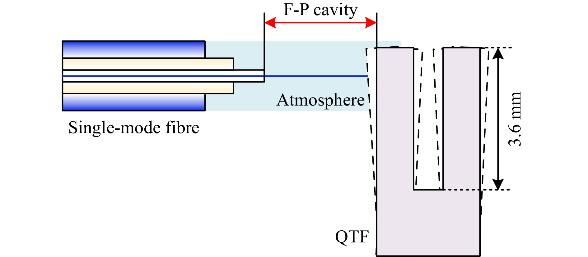
Fabry–Perot (F–P)-based phase demodulation of heterodyne light-induced thermoelastic spectroscopy (H-LITES) was demonstrated for the first time in this study. The vibration of a quartz tuning fork (QTF) was detected using the F–P interference principle instead of an electrical signal through the piezoelectric effect of the QTF in traditional LITES to avoid thermal noise. Given that an Fabry–Perot interferometer (FPI) is vulnerable to disturbances, a phase demodulation method that has been demonstrated theoretically and experimentally to be an effective solution for instability was used in H-LITES. The sensitivity of the F–P phase demodulation method based on the H-LITES sensor was not associated with the wavelength or power of the probe laser. Thus, stabilising the quadrature working point (Q-point) was no longer necessary. This new method of phase demodulation is structurally simple and was found to be resistant to interference from light sources and the surroundings using the LITES technique.

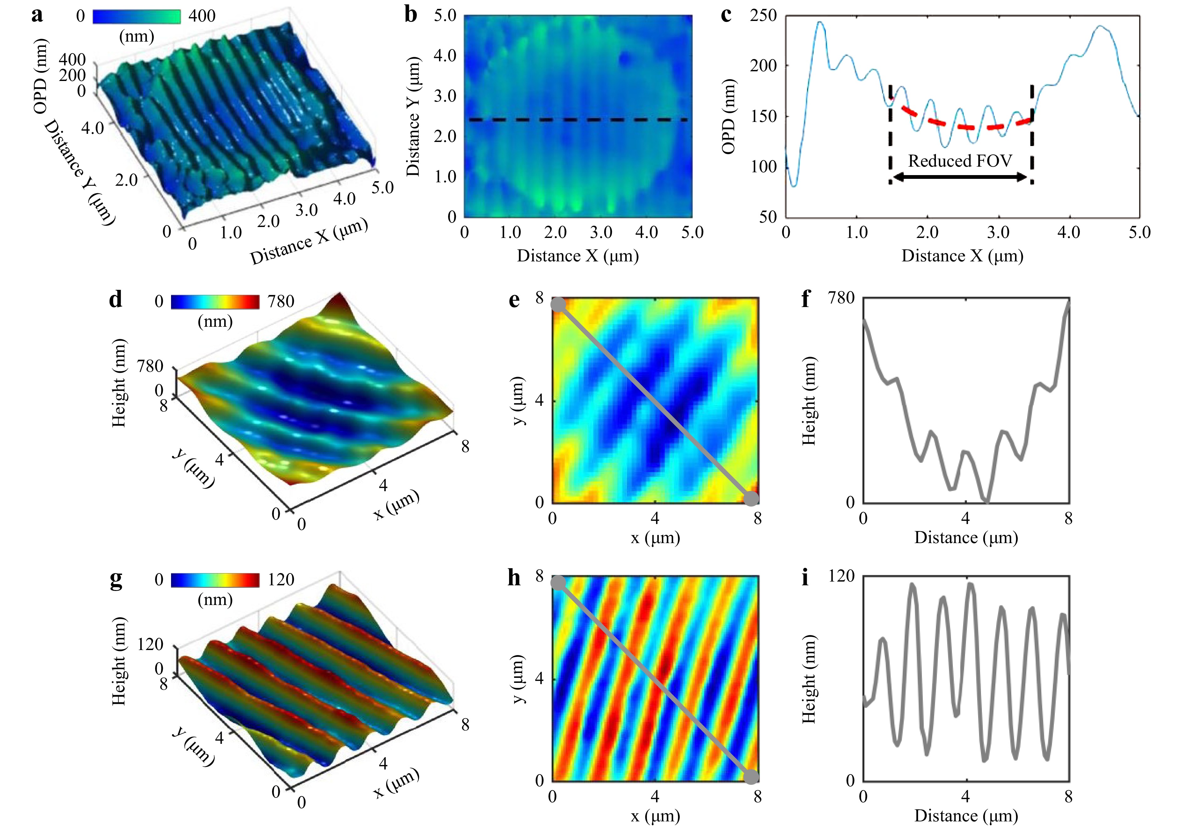
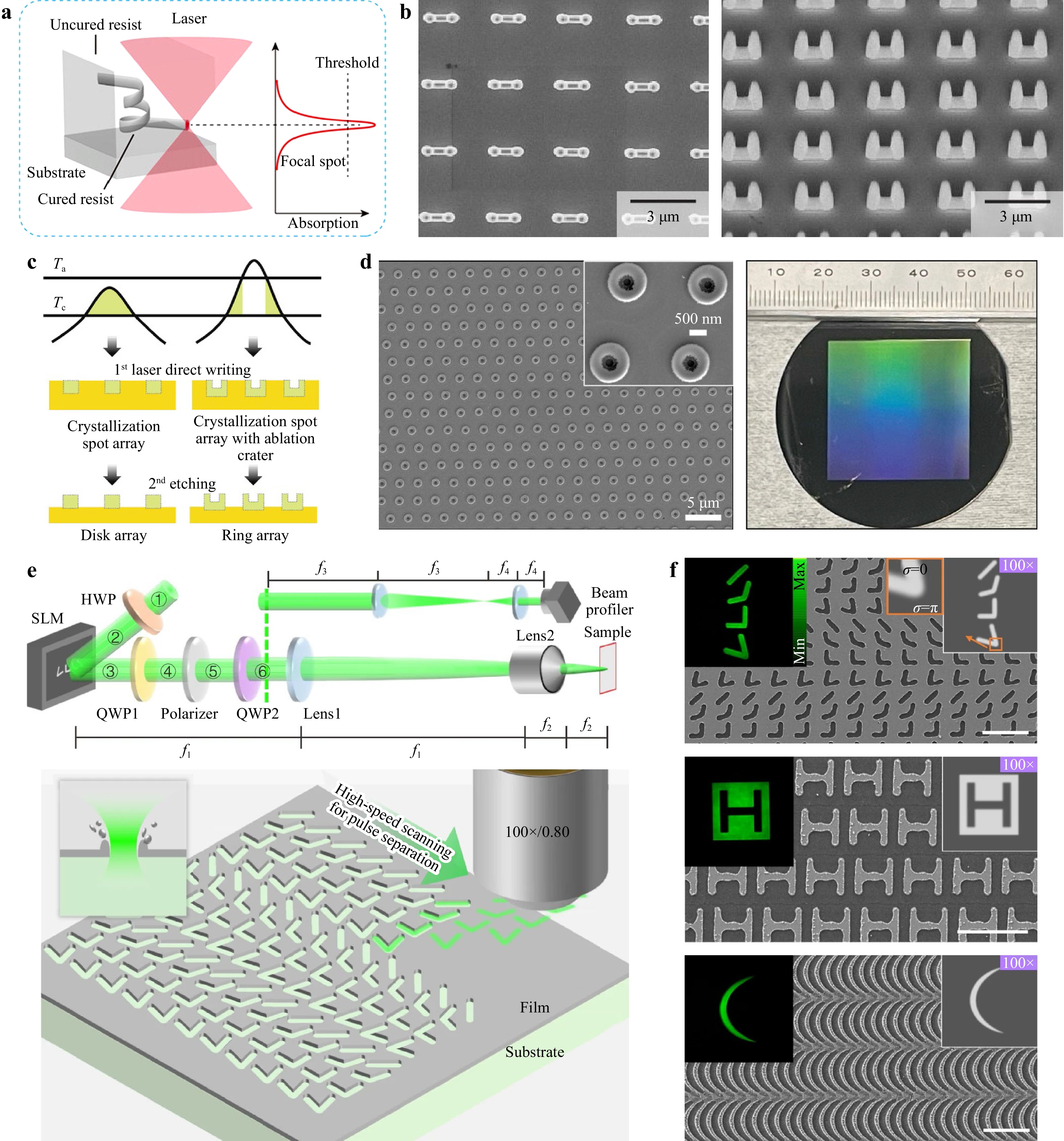
Organic proteins are attractive owing to their unique optical properties, remarkable mechanical characteristics, and biocompatibility. Manufacturing multifunctional structures on organic protein films is essential for practical applications; however, the controllable fabrication of specific structures remains challenging. Herein, we propose a strategy for creating specific structures on silk film surfaces by modulating the bulging and ablation of organic materials. Unique surface morphologies such as bulges and craters with continuously varying diameters were generated based on the controlled ultrafast laser-induced crystal-form transition and plasma ablation of the silk protein. Owing to the anisotropic optical properties of the bulge/crater structures with different periods, the fabricated organic films can be used for large-scale inkless color printing. By simultaneously engineering bulge/crater structures, we designed and demonstrated organic film-based optical functional devices that achieves holographic imaging and optical focusing. This study provides a promising strategy for the fabrication of multifunctional micro/nanostructures that can broaden the potential applications of organic materials.

We describe how a direct combination of an axicon and a lens can represent a simple and efficient beam-shaping solution for laser material processing applications. We produce high-angle pseudo-Bessel micro-beams at 1550 nm, which would be difficult to produce by other methods. Combined with appropriate stretching of femtosecond pulses, we access optimized conditions inside semiconductors allowing us to develop high-aspect-ratio refractive-index writing methods. Using ultrafast microscopy techniques, we characterize the delivered local intensities and the triggered ionization dynamics inside silicon with 200-fs and 50-ps pulses. While similar plasma densities are produced in both cases, we show that repeated picosecond irradiation induces permanent modifications spontaneously growing shot-after-shot in the direction of the laser beam from front-surface damage to the back side of irradiated silicon wafers. The conditions for direct microexplosion and microchannel drilling similar to those today demonstrated for dielectrics still remain inaccessible. Nonetheless, this work evidences higher energy densities than those previously achieved in semiconductors and a novel percussion writing modality to create structures in silicon with aspect ratios exceeding
700 without any motion of the beam. The estimated transient change of conductivity and measured ionization fronts at near luminal speed along the observed microplasma channels support the vision of vertical electrical connections optically controllable at GHz repetition rates. The permanent silicon modifications obtained by percussion writing are light-guiding structures according to a measured positive refractive index change exceeding
. These findings open the door to unique monolithic solutions for electrical and optical through-silicon-vias which are key elements for vertical interconnections in 3D chip stacks.

Mode-division multiplexing technology has been proposed as a crucial technique for enhancing communication capacity and alleviating growing communication demands. Optical switching, which is an essential component of optical communication systems, enables information exchange between channels. However, existing optical switching solutions are inadequate for addressing flexible information exchange among the mode channels. In this study, we introduced a flexible mode switching system in a multimode fibre based on an optical neural network chip. This system utilised the flexibility of on-chip optical neural networks along with an all-fibre orbital angular momentum (OAM) mode multiplexer-demultiplexer to achieve mode switching among the three OAM modes within a multimode fibre. The system adopted an improved gradient descent algorithm to achieve training for arbitrary 3×3 exchange matrices and ensured maximum crosstalk of less than -18.7 dB, thus enabling arbitrary inter-mode channel information exchange. The proposed optical-neural-network-based mode-switching system was experimentally validated by successfully transmitting different modulation formats across various modes. This innovative solution holds promise for providing effective optical switching in practical multimode communication networks.

Dwell time plays a vital role in determining the accuracy and convergence of the computer-controlled optical surfacing process. However, optimizing dwell time presents a challenge due to its ill-posed nature, resulting in non-unique solutions. To address this issue, several well-known methods have emerged, including the iterative, Bayesian, Fourier transform, and matrix-form methods. Despite their independent development, these methods share common objectives, such as minimizing residual errors, ensuring dwell time's positivity and smoothness, minimizing total processing time, and enabling flexible dwell positions. This paper aims to comprehensively review the existing dwell time optimization methods, explore their interrelationships, provide insights for their effective implementations, evaluate their performances, and ultimately propose a unified dwell time optimization methodology.

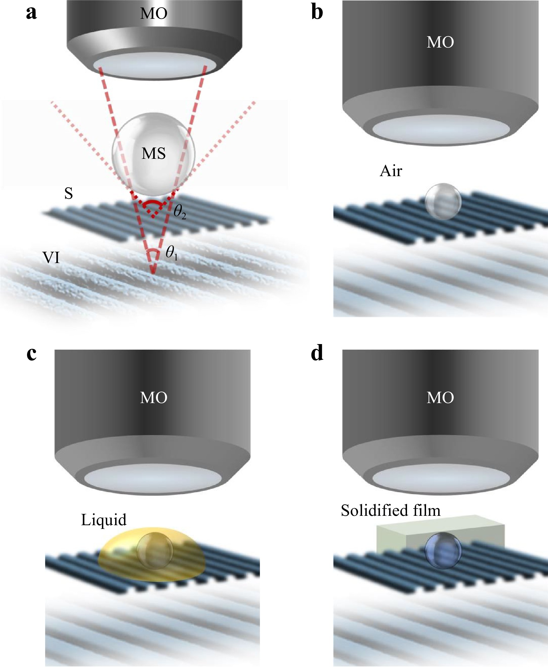
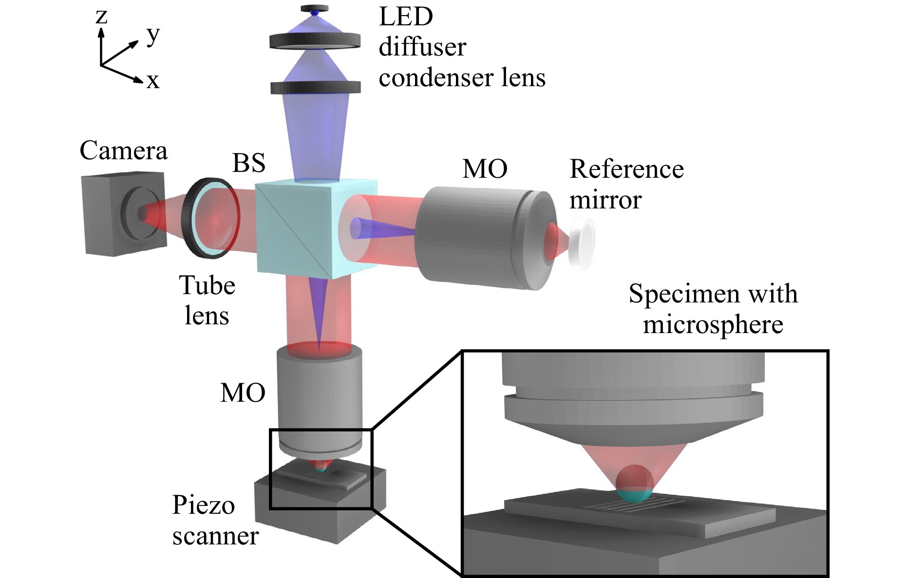
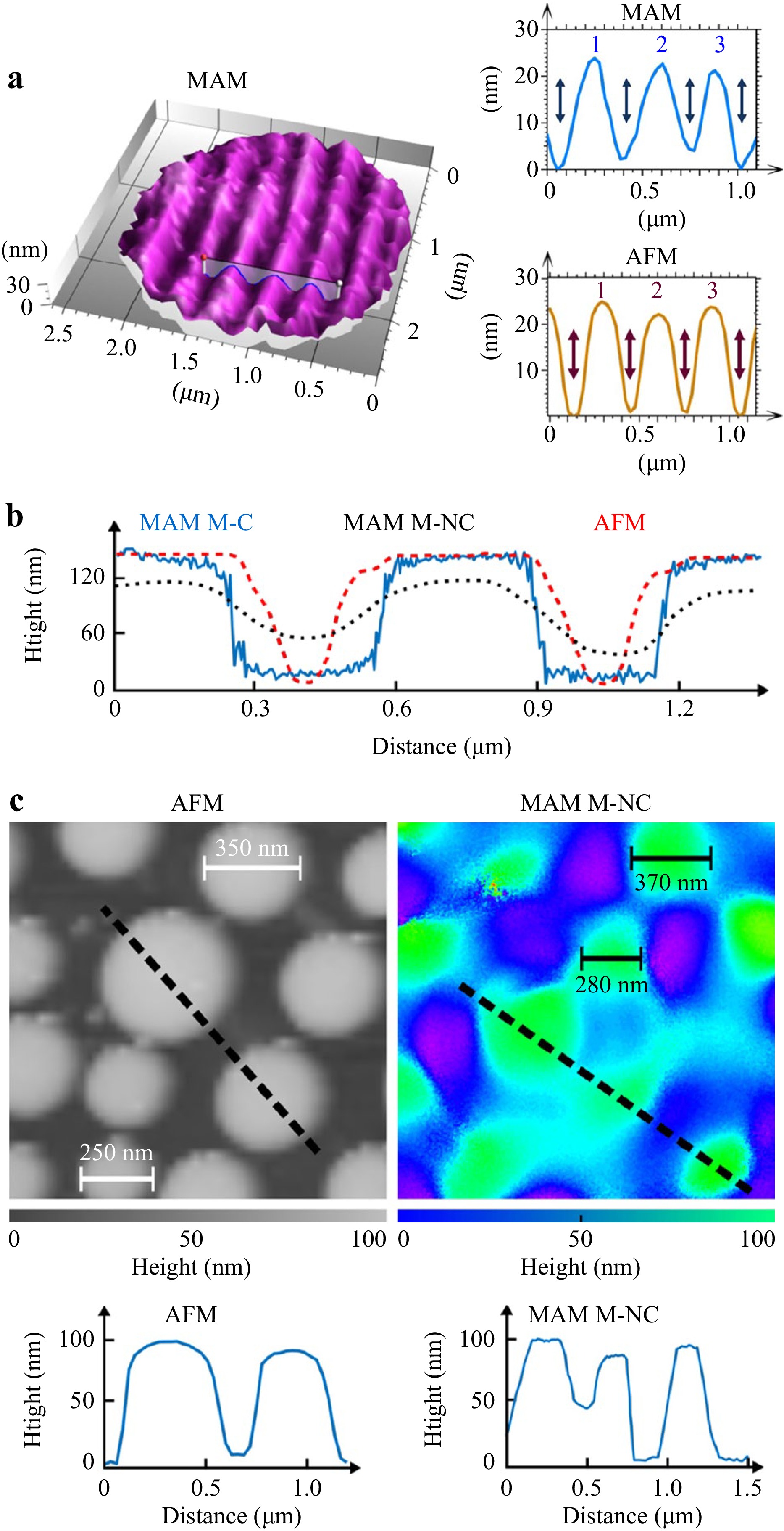
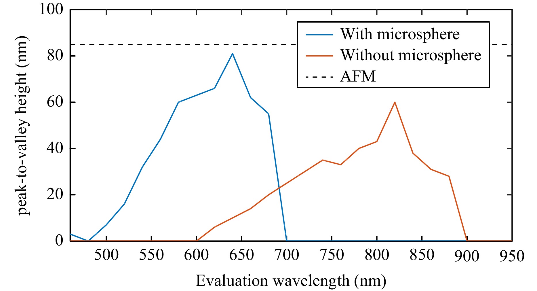
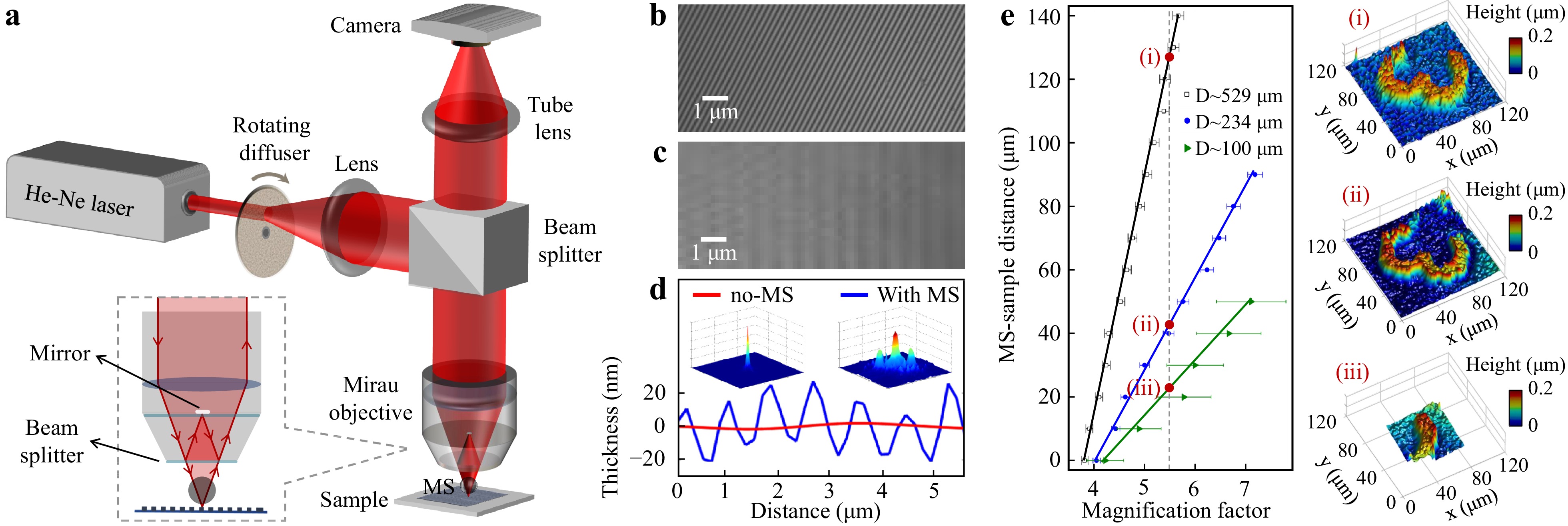
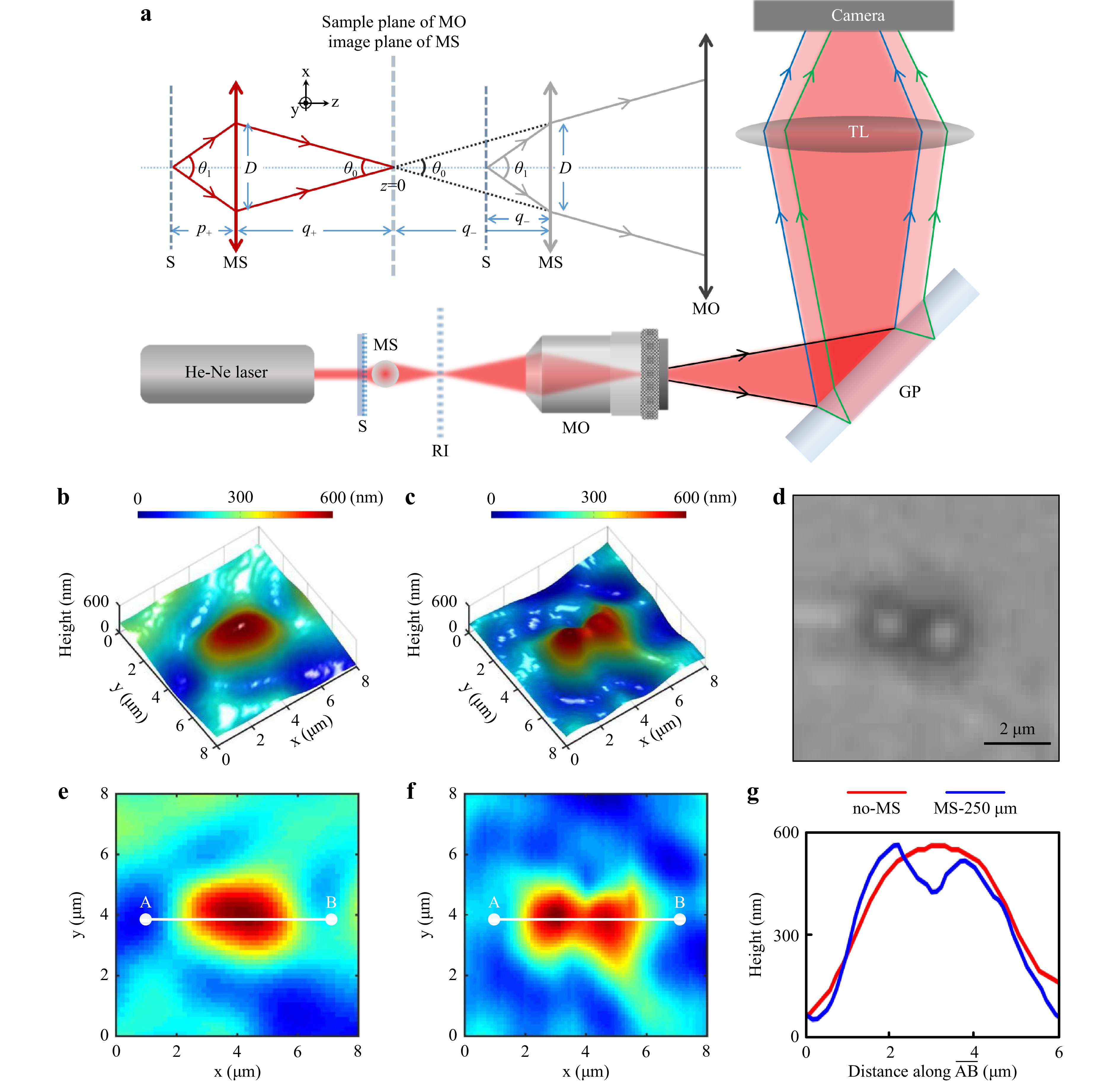
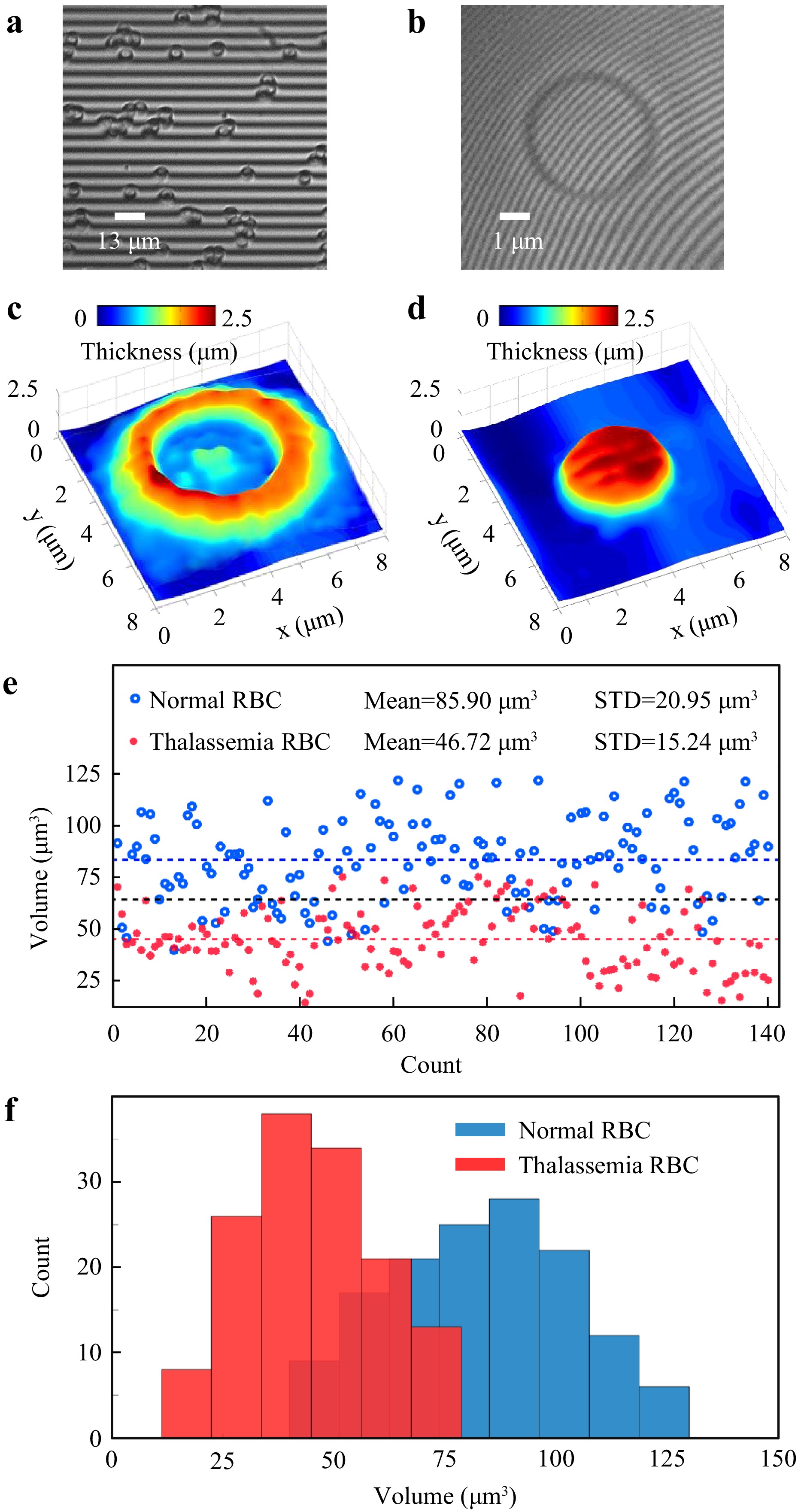
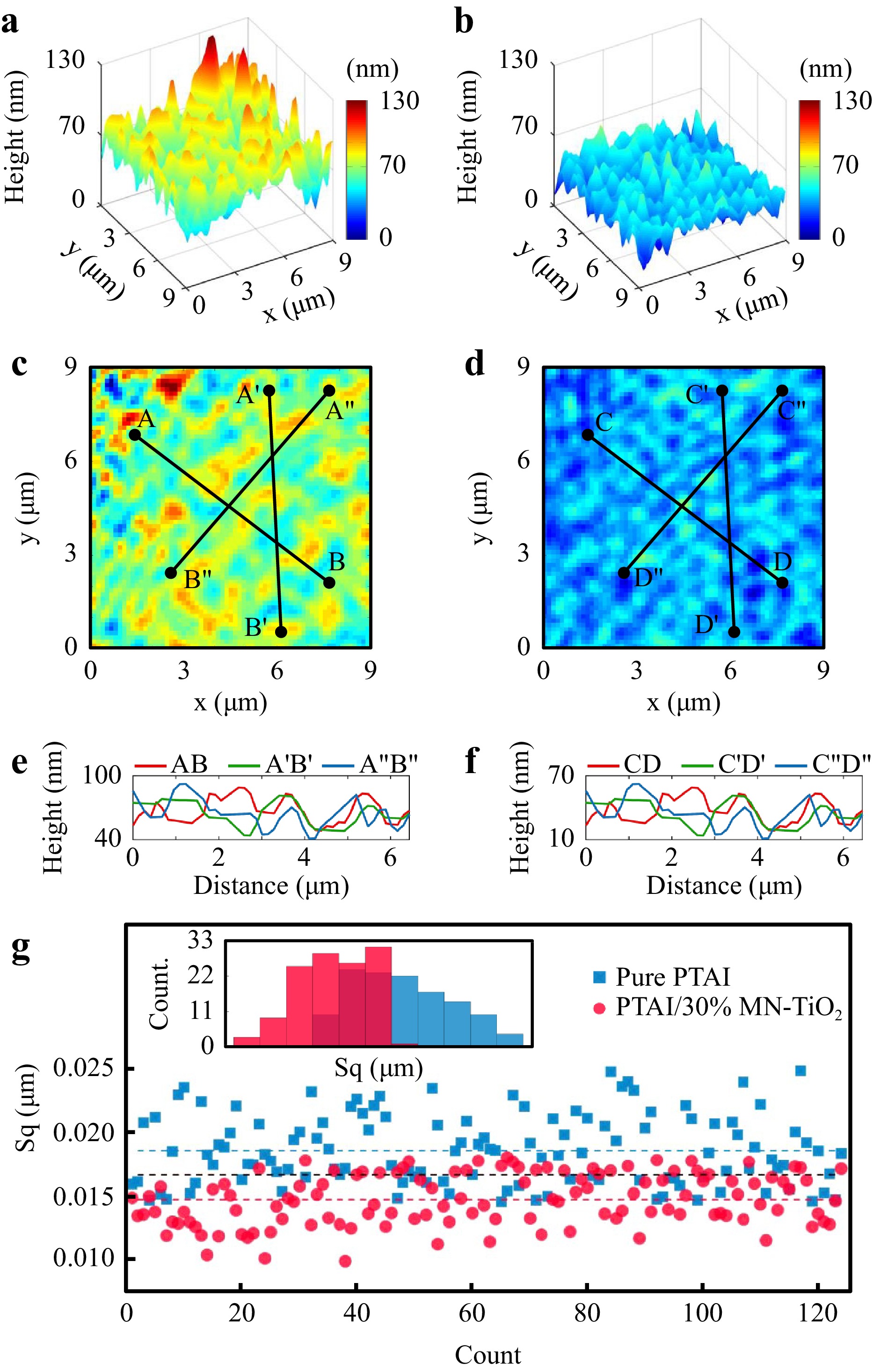
Although optical microscopy is a widely used technique across various multidisciplinary fields for inspecting small-scale objects, surfaces or organisms, it faces a significant limitation: the lateral resolution of optical microscopes is fundamentally constrained by light diffraction. Dielectric micro-spheres, however, offer a promising solution to this issue as they are capable of significantly enhancing lateral resolution through extraordinary phenomena, such as a photonic nanojet. Building upon the potential of dielectric micro-spheres, this paper introduces a novel approach for fabricating 3D micro-devices designed to enhance lateral resolution in optical microscopy. The proposed 3D micro-device comprises a modified coverslip and a micro-sphere, facilitating easy handling and integration into any existing optical microscope. To manufacture the device, two advanced femtosecond laser techniques are employed: femtosecond laser ablation and multi-photon lithography. Femtosecond laser ablation was employed to create a micro-hole in the coverslip, which allows light to be focused through this aperture. Multi-photon lithography was used to fabricate a micro-sphere with a diameter of 20 µm, along with a cantilever that positions the above the processed micro-hole and connect it with the coverslip. In this context, advanced processing strategies for multi-photon lithography to produce a micro-sphere with superior surface roughness and almost perfect geometry (λ/8) from a Zr-based hybrid photoresist are demonstrated. The performance of the micro-device was evaluated using Mirau-type coherence scanning interferometry in conjunction with white light illumination at a central wavelength of 600 nm and a calibration grid (Λ = 0.28 µm, h > 50 nm). Here, the 3D micro-device proved to be capable of enhancing lateral resolution beyond the limits achievable with conventional lenses or microscope objectives when used in air. Simultaneously, it maintained the high axial resolution characteristic of Mirau-type coherence scanning interferometry. The results and optical properties of the micro-sphere were analyzed and further discussed through simulations.

Optical micro/nanofibers (MNFs) taper-drawn from silica fibers possess intriguing optical and mechanical properties. Recently, MNF array or MNFs with identical geometries have been attracting more and more attention, however, current fabrication technique can draw only one MNF at a time, with a low drawing speed (typically 0.1 mm/s) and a complicated process for high-precision control, making it inefficient in fabricating multiple MNFs. Here, we propose a parallel-fabrication approach to simultaneously drawing multiple (up to 20) MNFs with almost identical geometries. For fiber diameter larger than 500 nm, measured optical transmittances of all as-drawn MNFs exceed 96.7% at 1550-nm wavelength, with a diameter deviation within 5%. Our results pave a way towards high-yield fabrication of MNFs that may find applications from MNF-based optical sensors, optical manipulation to fiber-to-chip interconnection.

Microring resonators have been widely used to fabricate passive optical devices such as wavelength division multiplexers, differentiators, and integrators. Research on terahertz (THz) components has been accelerated by these photonics technologies, and compact and integrated time-domain differentiator that enable low-loss, high-speed THz signal processing, and can be packaged for THz applications are necessary. In this study, an on-chip THz temporal differentiator based on all-silicon photonic technology was developed. This device primarily consisted of a microring waveguide resonator and was packaged with standard waveguide compatibility. The device performed time-domain differentiation on input signals at a frequency of 405.45 GHz and an insertion loss and a working bandwidth of 2.5 dB and 0.36 GHz, respectively. The differentiator handled various periodic waveforms. The device performed as an edge detector, which detected step-like edges in high-speed input signals through differential effects. This development holds significant promise for future THz data processing technologies and THz communication systems.

Achieving a high sensitivity for practical applications has always been one of the main developmental directions for wearable flexible pressure sensors. This paper introduces a laser speckle grayscale lithography system and a novel method for fabricating random conical array microstructures using grainy laser speckle patterns. Its feasibility is attributed to the autocorrelation function of the laser speckle intensity, which adheres to a first-order Bessel function of the first kind. Through objective speckle size and exposure dose manipulations, we developed a microstructured photoresist with various micromorphologies. These microstructures were used to form polydimethylsiloxane microstructured electrodes that were used in flexible capacitive pressure sensors. These sensors exhibited an ultra-high sensitivity: 19.76 kPa-1 for the low-pressure range of 0–100 Pa. Their minimum detection threshold was 1.9 Pa, and they maintained stability and resilience over 10,000 test cycles. These sensors proved to be adept at capturing physiological signals and providing tactile feedback, thereby emphasizing their practical value.

The mode-division multiplexing technique combined with a few-mode erbium-doped fiber amplifier (FM-EDFA) demonstrates significant potential for solving the capacity limitation of standard single-mode fiber (SSMF) transmission systems. However, the differential mode gain (DMG) arising in the FM-EDFA fundamentally limits its transmission capacity and length. Herein, an innovative DMG equalization strategy using femtosecond laser micromachining to adjust the refractive index (RI) is presented. Variable mode-dependent attenuations can be achieved according to the DMG profile of the FM-EDFA, enabling DMG equalization. To validate the proposed strategy, DMG equalization of the commonly used FM-EDFA configuration was investigated. Simulation results revealed that by optimizing both the length and RI modulation depth of the femtosecond laser-tailoring area, the maximum DMG (DMGmax) among the three linear-polarized (LP) mode-group was mitigated from 10 dB to 1.52 dB, whereas the average DMG (DMGave) over the C-band was reduced from 8.95 dB to 0.78 dB. Finally, a 2-LP mode-group DMG equalizer was experimentally demonstrated, resulting in a reduction of the DMGmax from 2.09 dB to 0.46 dB, and a reduction of DMGave over the C band from 1.64 dB to 0.26 dB, with only a 1.8-dB insertion loss. Moreover, a maximum range of variable DMG equalization was achieved with 5.4 dB, satisfying the requirements of the most commonly used 2-LP mode-group amplification scenarios.

Minimally invasive endoscopy offers a high potential for biomedical imaging applications. However, conventional fiberoptic endoscopes require lens systems which are not suitable for real-time 3D imaging. Instead, a diffuser is utilized for passively encoding incoherent 3D objects into 2D speckle patterns. Neural networks are employed for fast computational image reconstruction beyond the optical memory effect. In this paper, we demonstrate single-shot 3D incoherent fiber imaging with keyhole access at video rate. Applying the diffuser fiber endoscope for fluorescence imaging is promising for in vivo deep brain diagnostics with cellular resolution.

Speckle patterns generated by the intermodal interference of multimode fibers enable accurate broadband wavelength measurements. However, the measurement speed is limited by the frame rate of the camera that captures the patterns. We propose a compact and cost-effective ultrafast wavemeter based on multimode and multicore fibers, which employs spectral–spatial–temporal mapping. The speckle patterns generated by multimode fibers enable spectral-to-spatial mapping, which is then sampled by a multicore fiber into a pulse sequence to implement spatial-to-temporal mapping. A high-speed single-pixel photodetector is employed to capture the pulse sequence, which is analysed using a multilayer perceptron to estimate the wavelength. The feasibility of the proposed wavelength estimation method is experimentally verified, achieving a measurement rate of 100 MHz with a resolution of 2.7 pm in a 1 nm operation bandwidth.
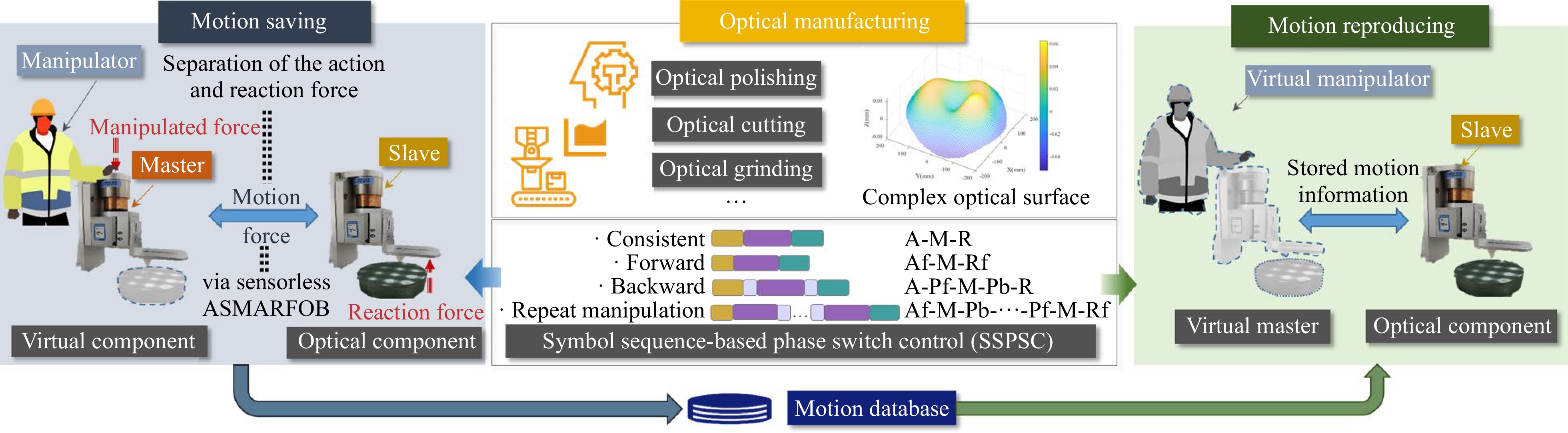
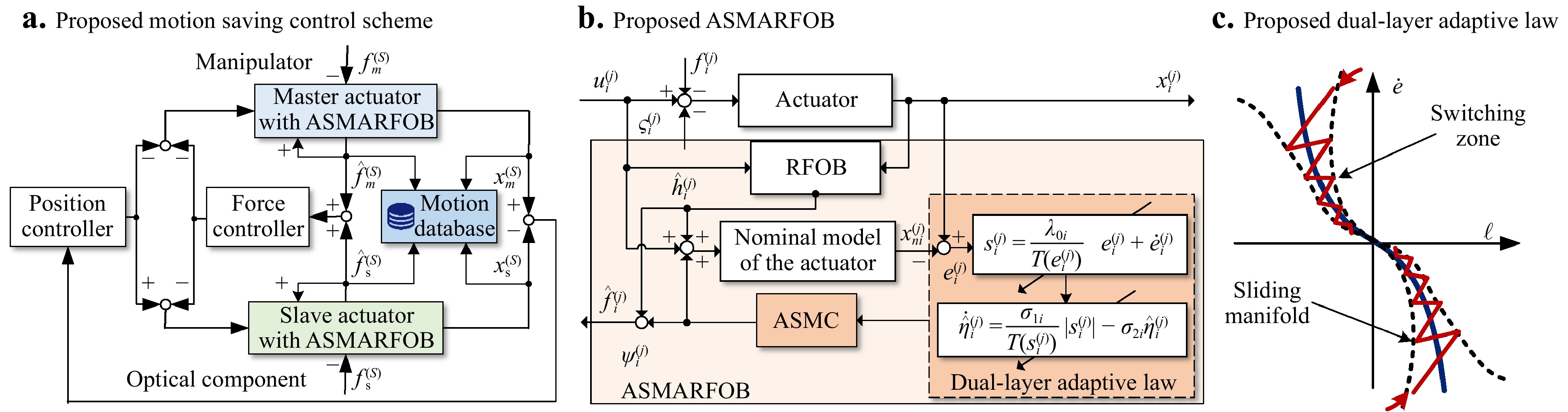
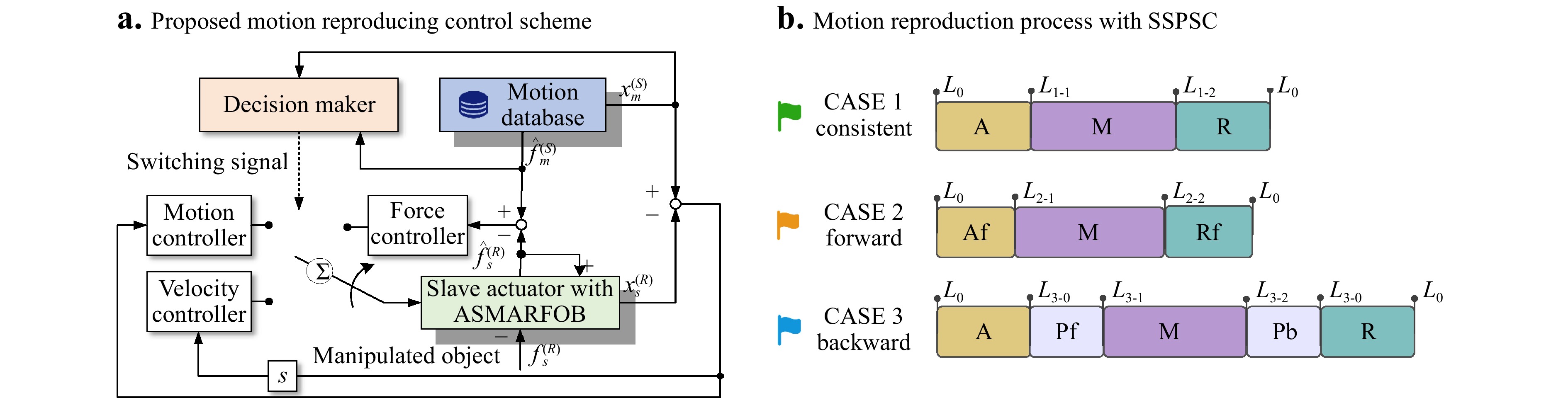
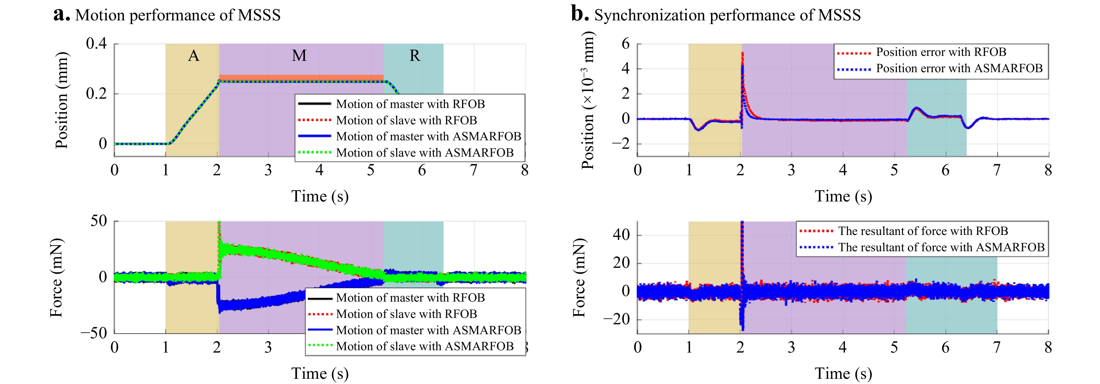
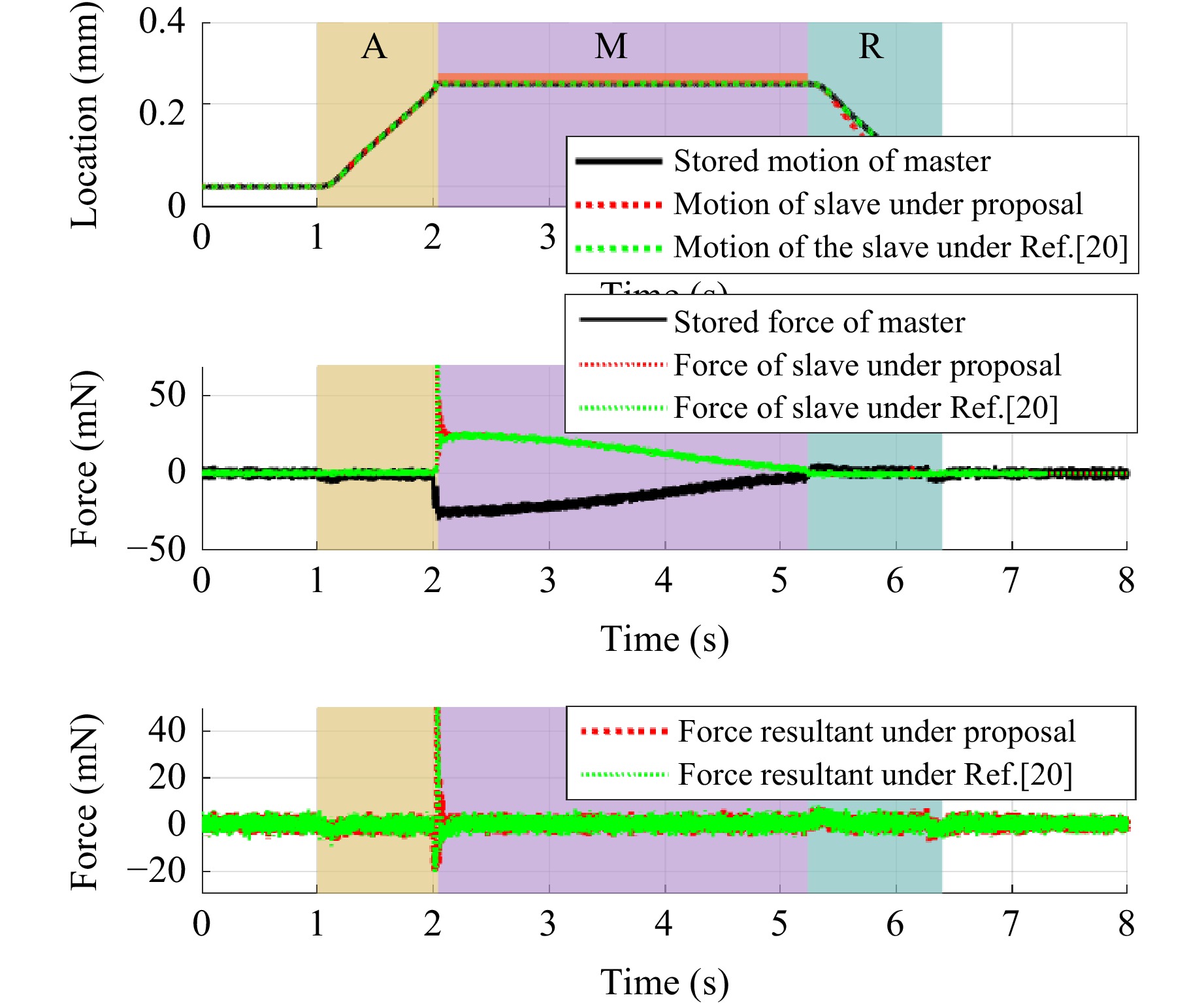
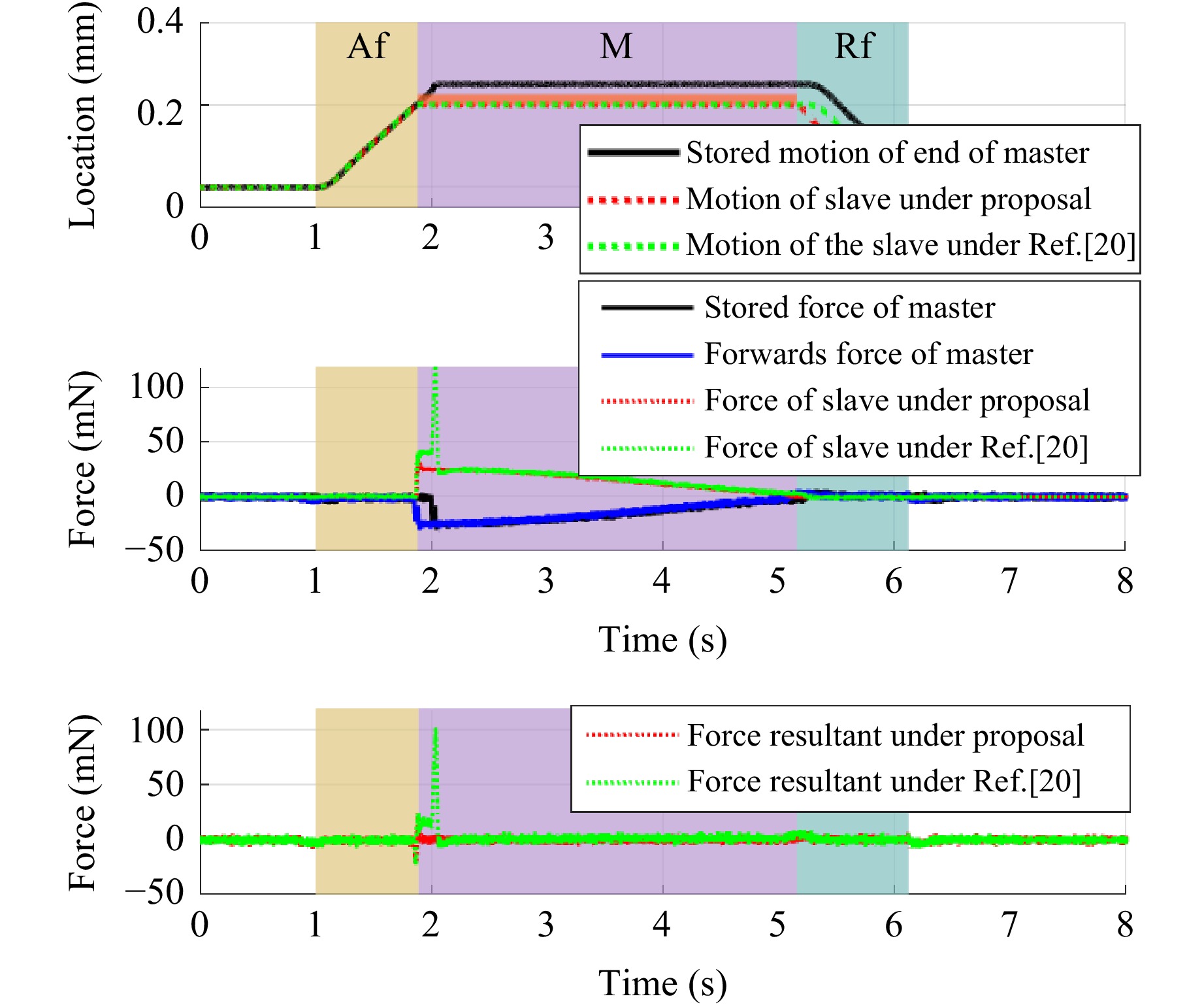
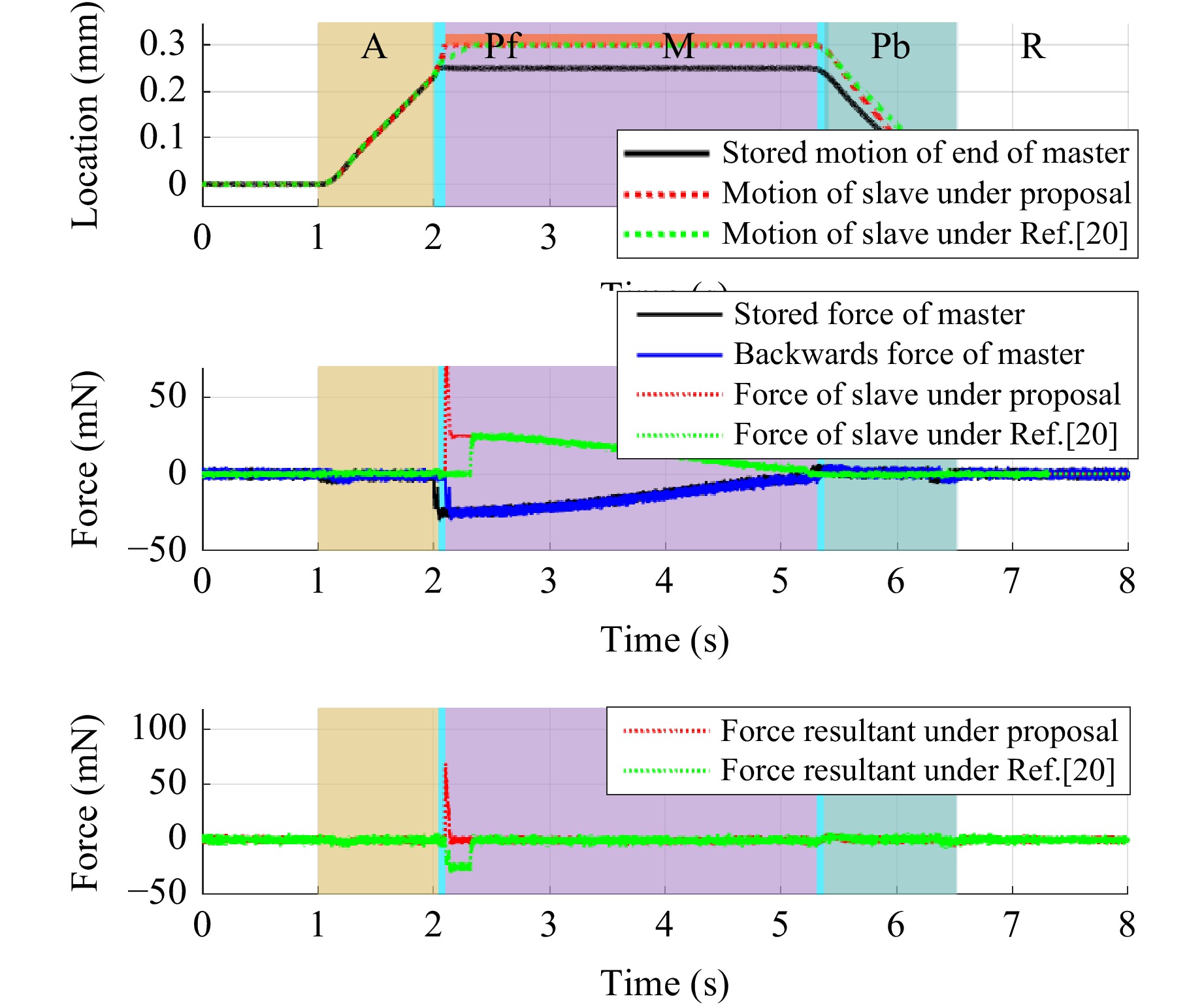
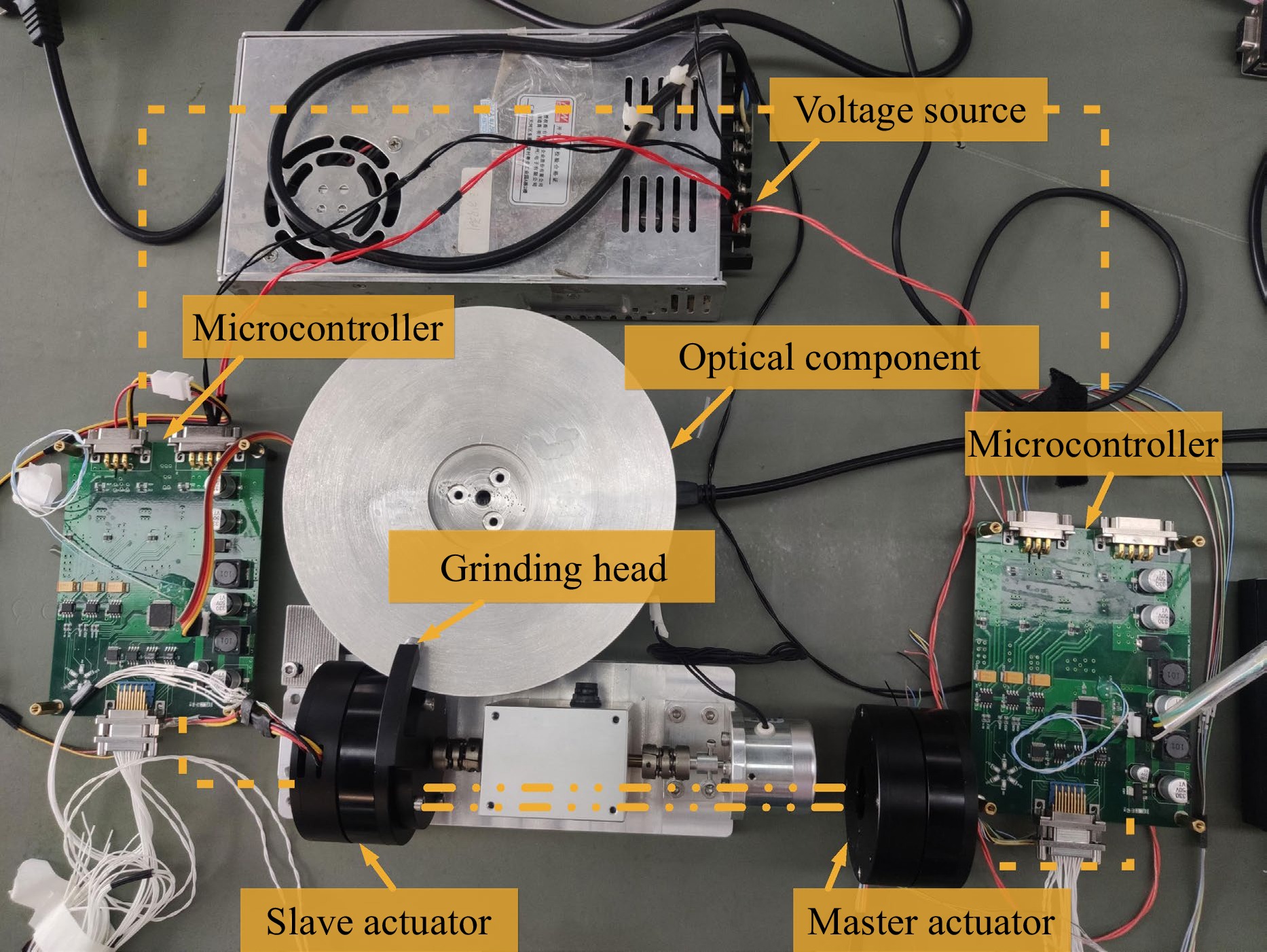
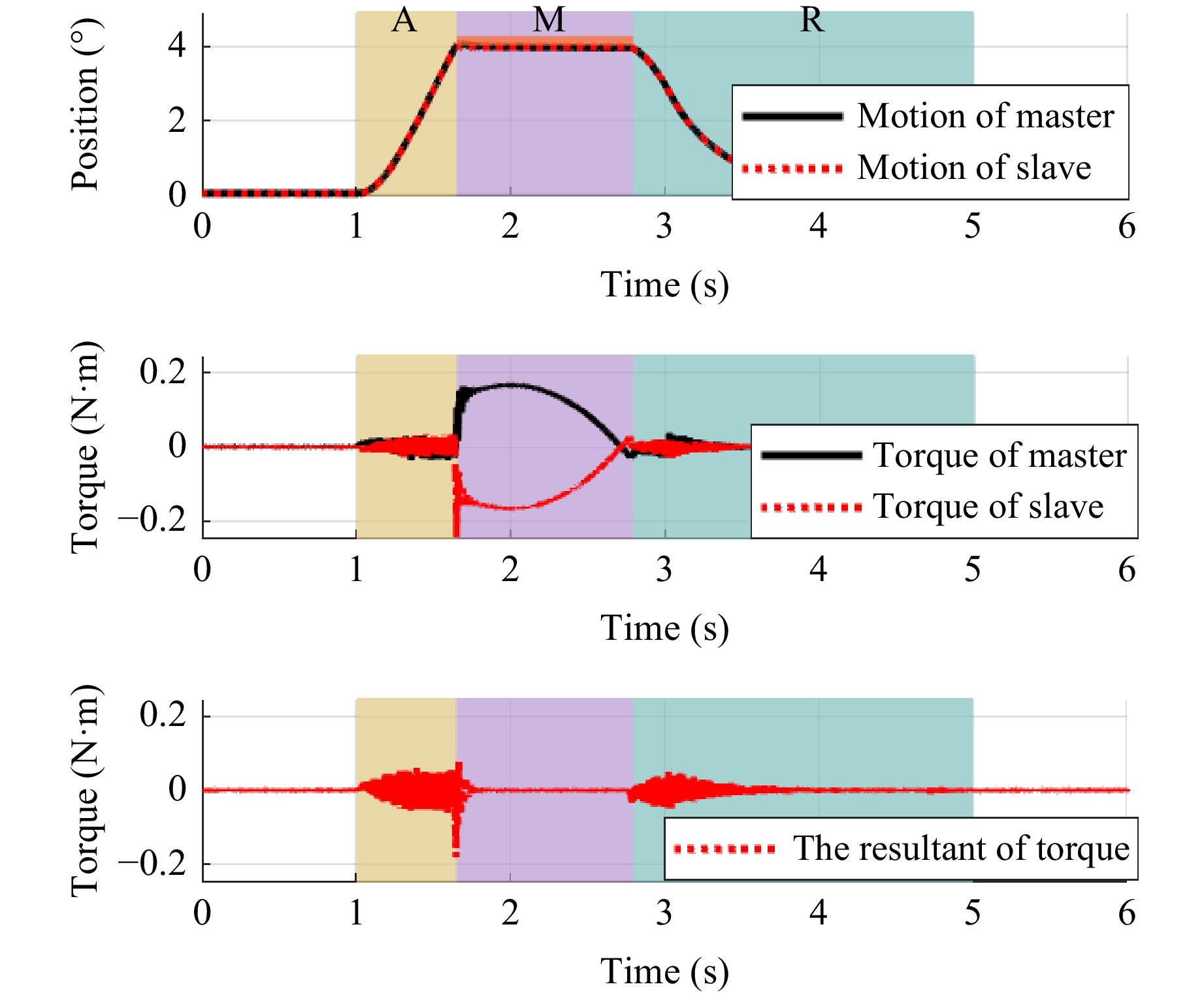
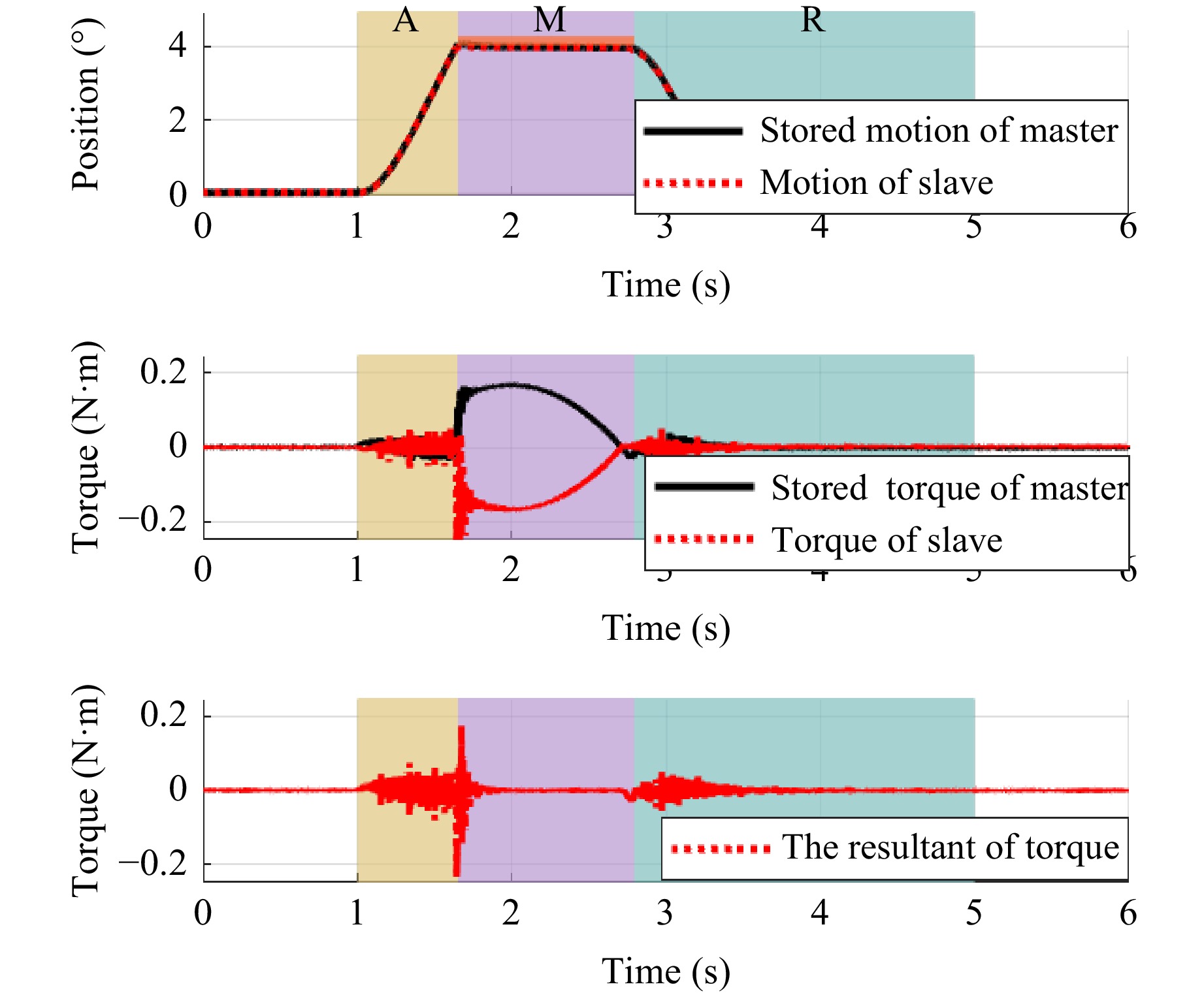
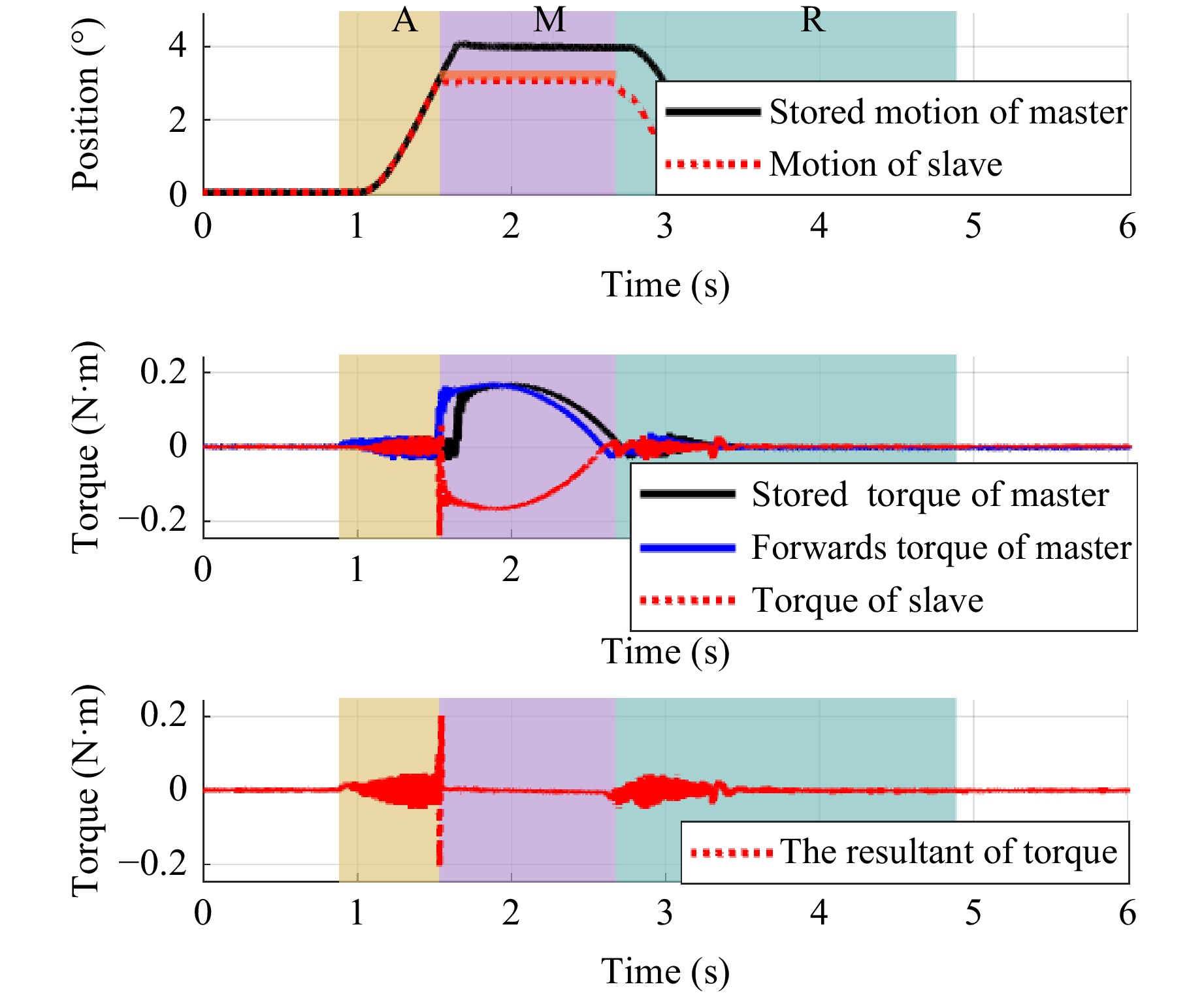
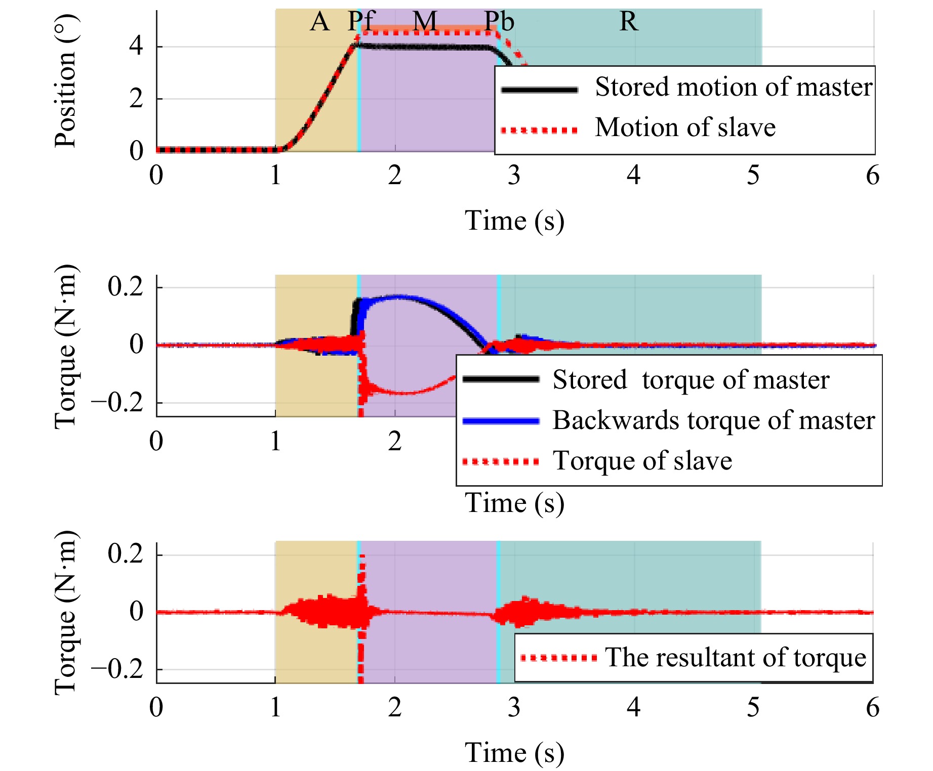
Implementation of robot-based motion control in optical machining demonstrably enhances the machining quality. The introduction of motion-copying method enables learning and replicating manipulation from experienced technicians. Nevertheless, the location uncertainties of objects and frequent switching of manipulated spaces in practical applications impose constraints on their further advancement. To address this issue, a motion-copying system with a symbol-sequence-based phase switch control (SSPSC) scheme was developed by transferring the operating skills and intelligence of technicians to mechanisms. The manipulation process is decomposed, symbolised, rearranged, and reproduced according to the manufacturing characteristics regardless of the change in object location. A force-sensorless adaptive sliding-mode-assisted reaction force observer (ASMARFOB), wherein a novel dual-layer adaptive law was designed for high-performance fine force sensing, was established. The uniformly ultimate boundedness (UUB) of the ASMARFOB is guaranteed based on the Lyapunov stability theory, and the switching stability of the SSPSC was examined. Validation simulations and experiments demonstrated that the proposed method enables better motion reproduction with high consistency and adaptability. The findings of this study can provide effective theoretical and practical guidance for high-precision intelligent optical manufacturing.
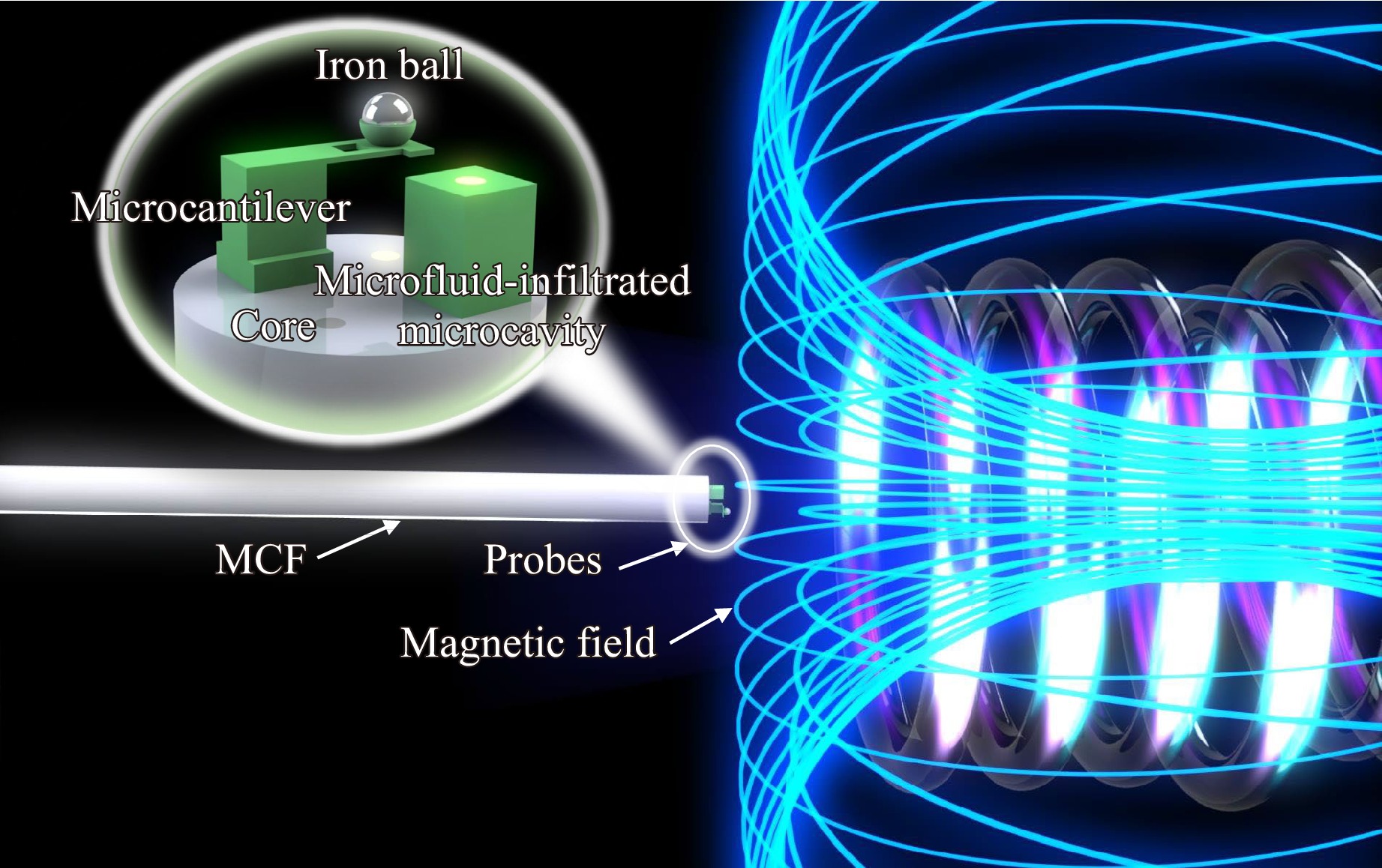
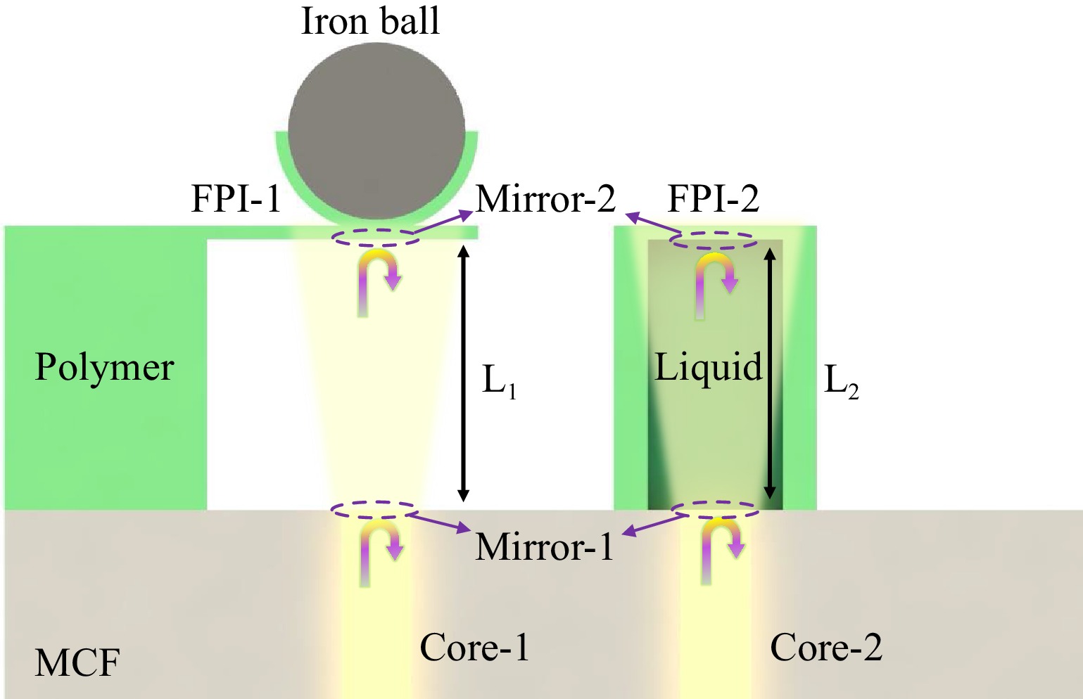
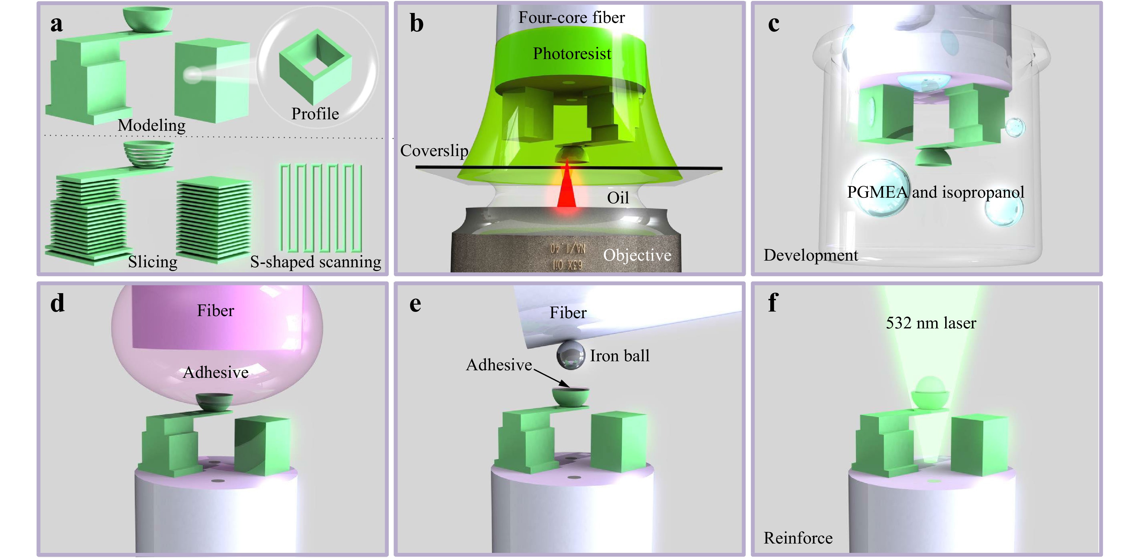
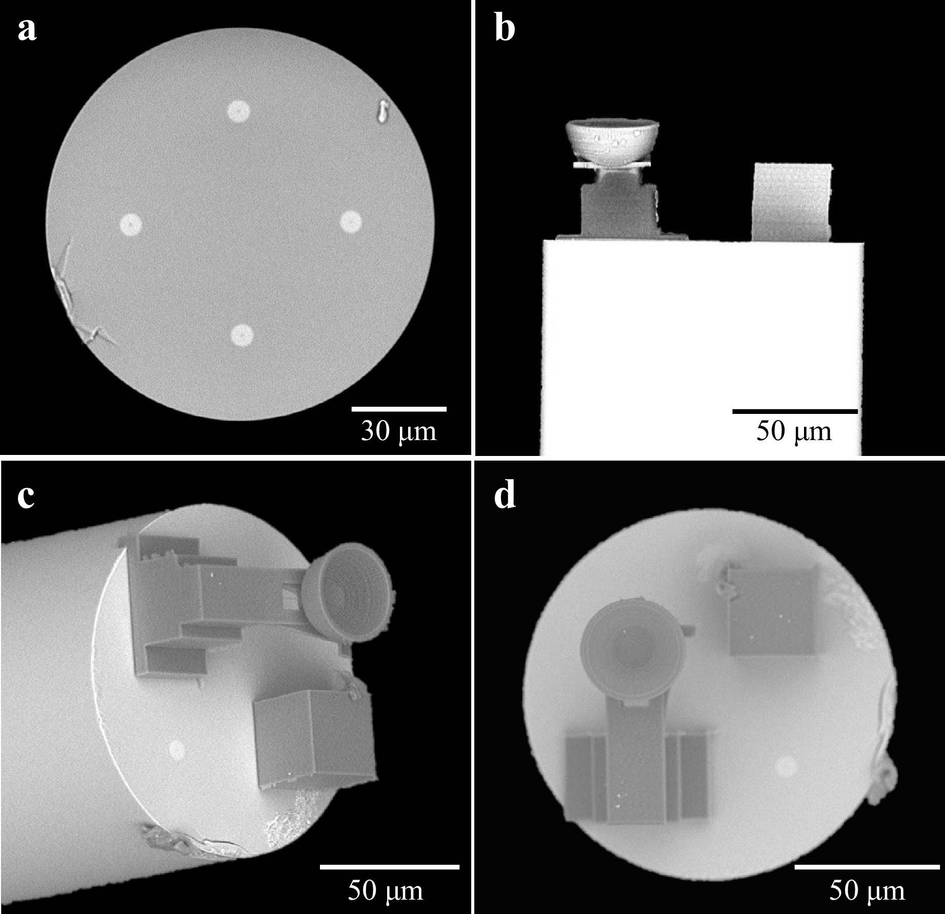
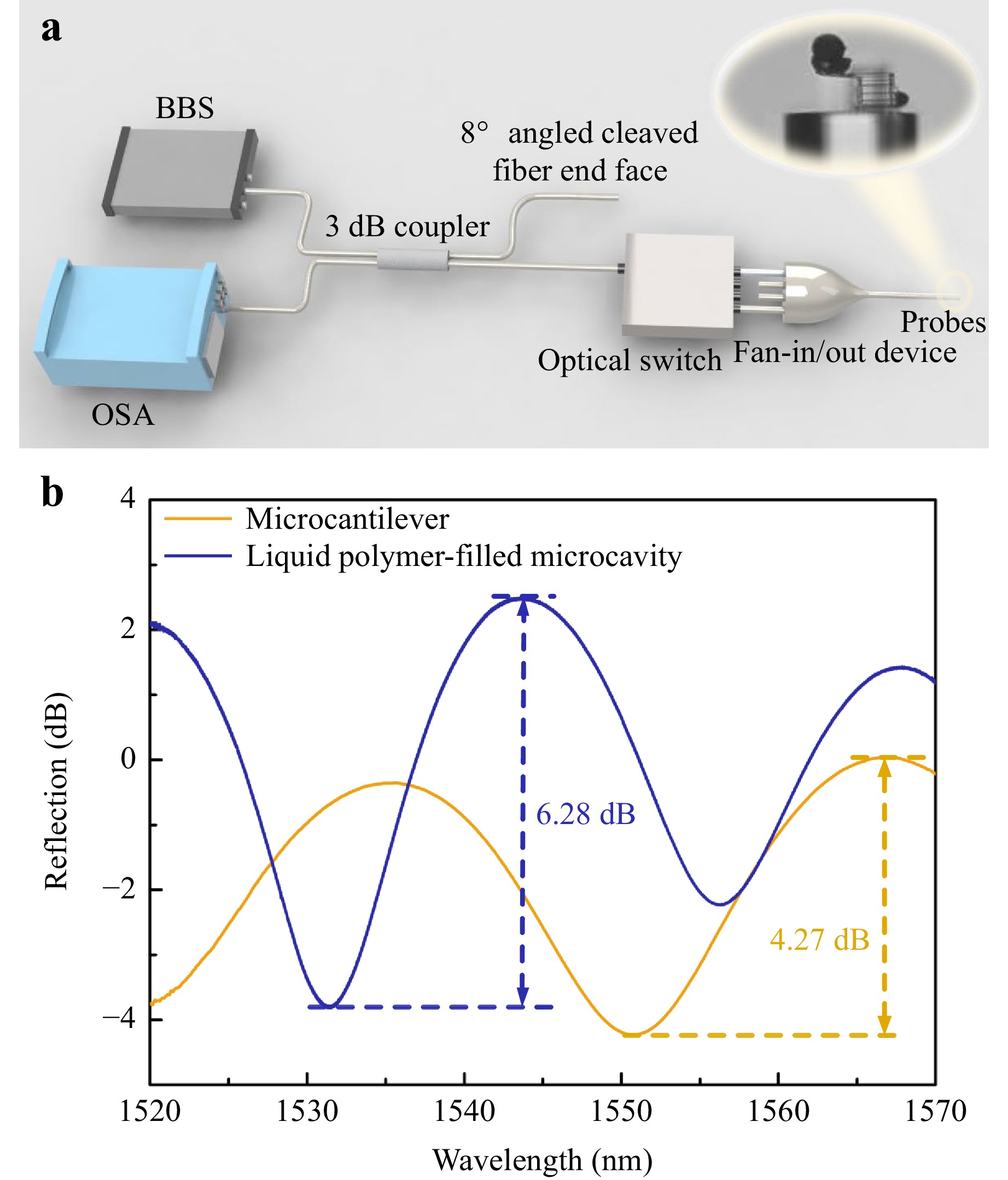
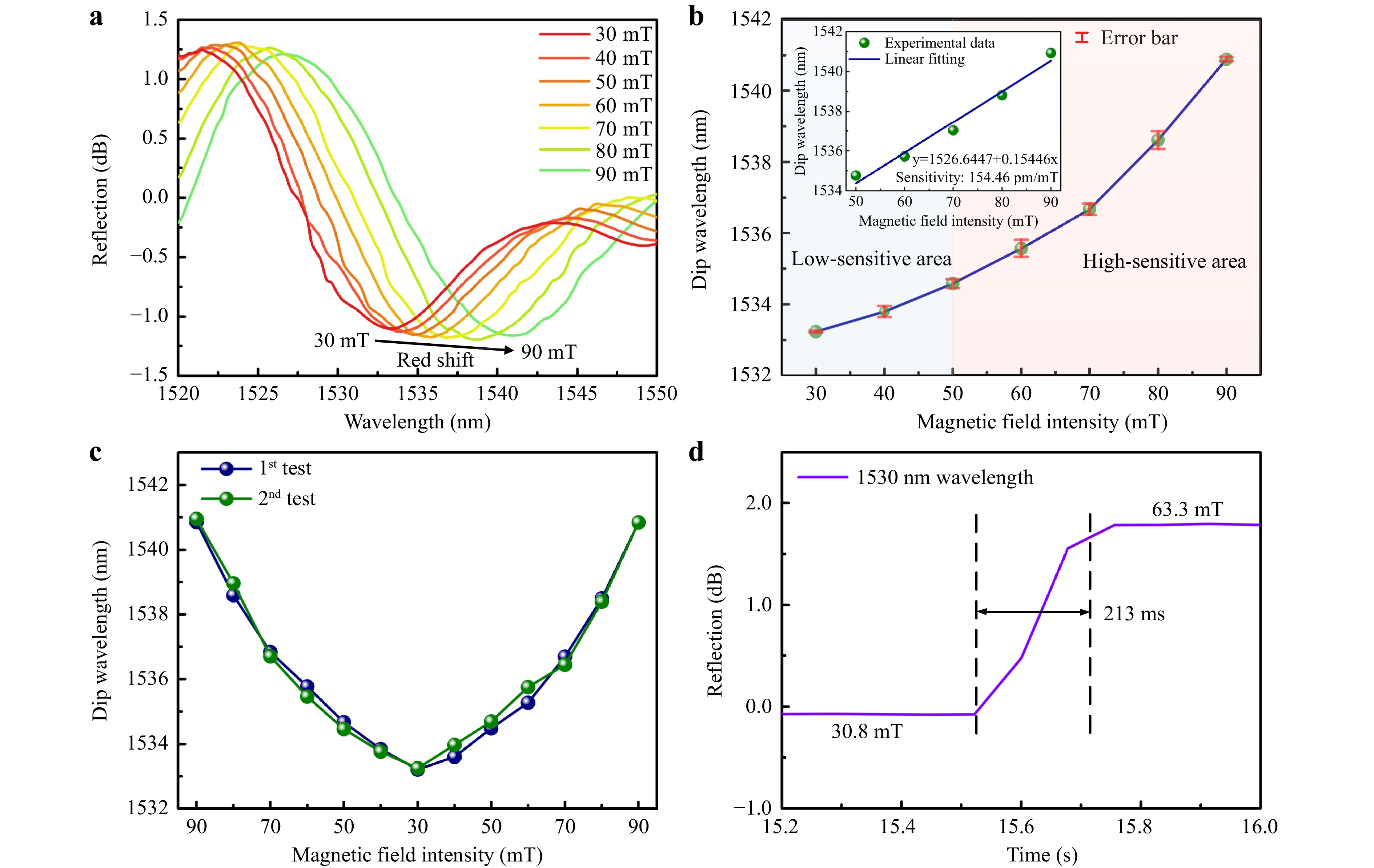
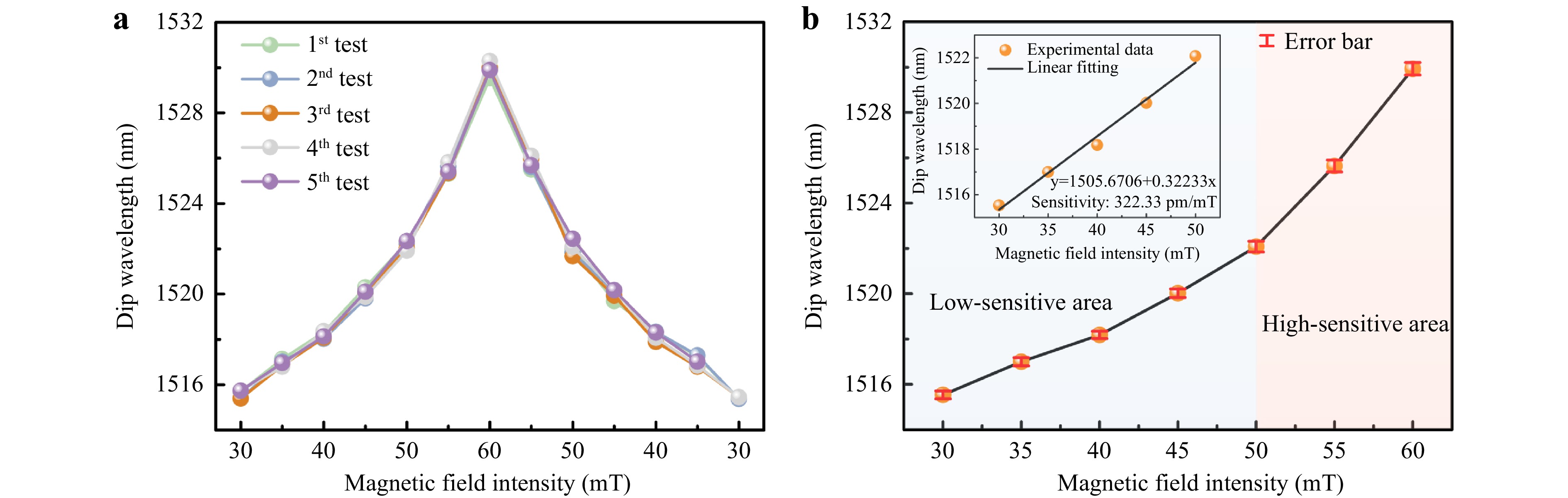
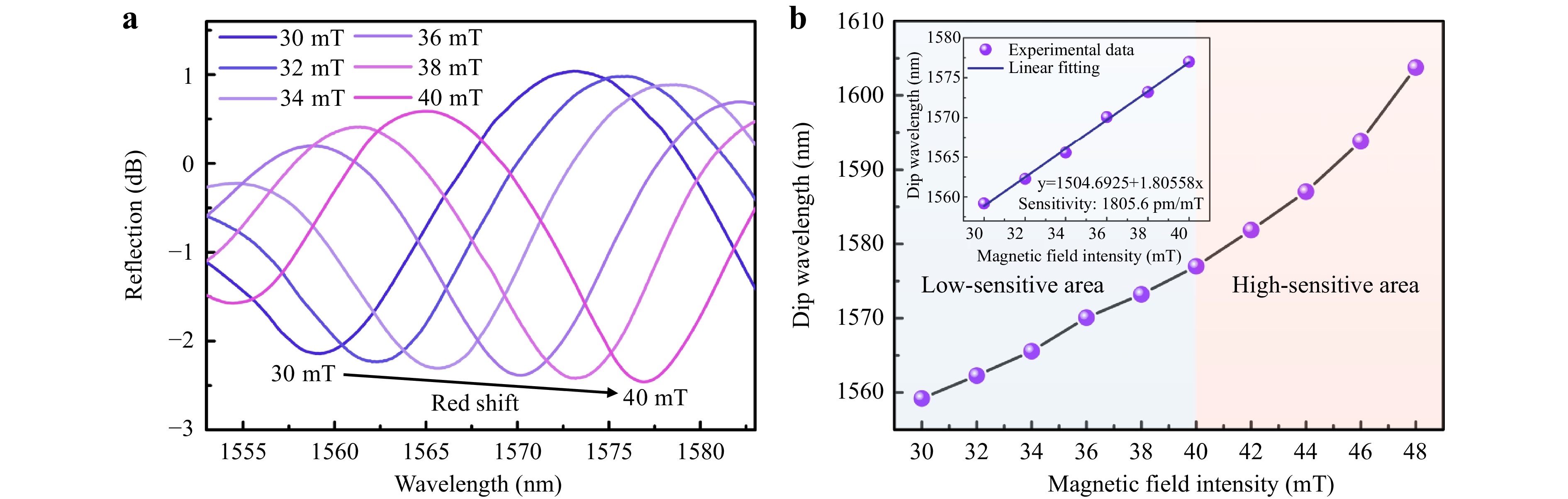
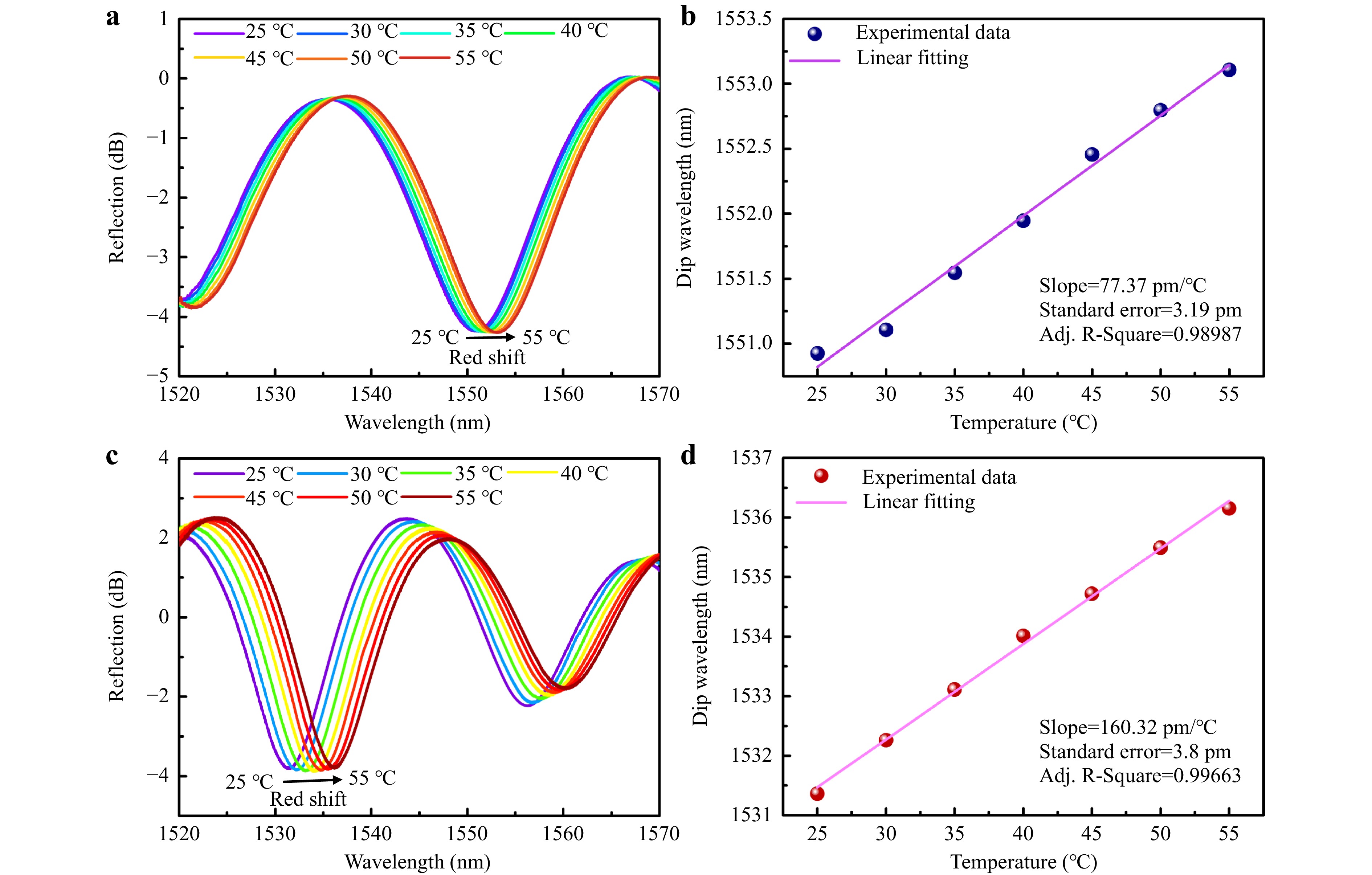
Miniaturized fiber-optic magnetic field sensors have attracted considerable interest owing to their superiorities in anti-electromagnetic interference and compactness. However, the intrinsic thermodynamic properties of the material make temperature cross-sensitivity a challenging problem in terms of sensing accuracy and reliability. In this study, an ultracompact multicore fiber (MCF) tip sensor was designed to discriminatively measure the magnetic field and temperature, which was subsequently evaluated experimentally. The novel 3D printed sensing component consists of a bowl-shaped microcantilever and a polymer microfluid-infiltrated microcavity on the end-facet of an MCF, acting as two miniaturized Fabry-Perot interferometers. The magnetic sensitivity of the microcantilever was implemented by incorporating an iron micro ball into the microcantilever, and the microfluid-infiltrated microcavity enhanced the capability of highly sensitive temperature sensing. Using this tiny fiber-facet device in the two channels of an MCF allows discriminative measurements of the magnetic field and temperature by determining the sensitivity coefficient matrix of two parameters. The device exhibited a high magnetic field intensity sensitivity, approximately 1805.6 pm/mT with a fast response time of ~ 213 ms and a high temperature sensitivity of 160.3 pm/℃. Moreover, the sensor had a low condition number of 11.28, indicating high reliability in two-parameter measurements. The proposed 3D printed MCF-tip probes, which detect multiple signals through multiple channels within a single fiber, can provide an ultracompact, sensitive, and reliable scheme for discriminative measurements. The bowl-shaped microcantilever also provides a useful platform for incorporating microstructures with functional materials, extending multi-parameter sensing scenarios and promoting the application of MCFs.
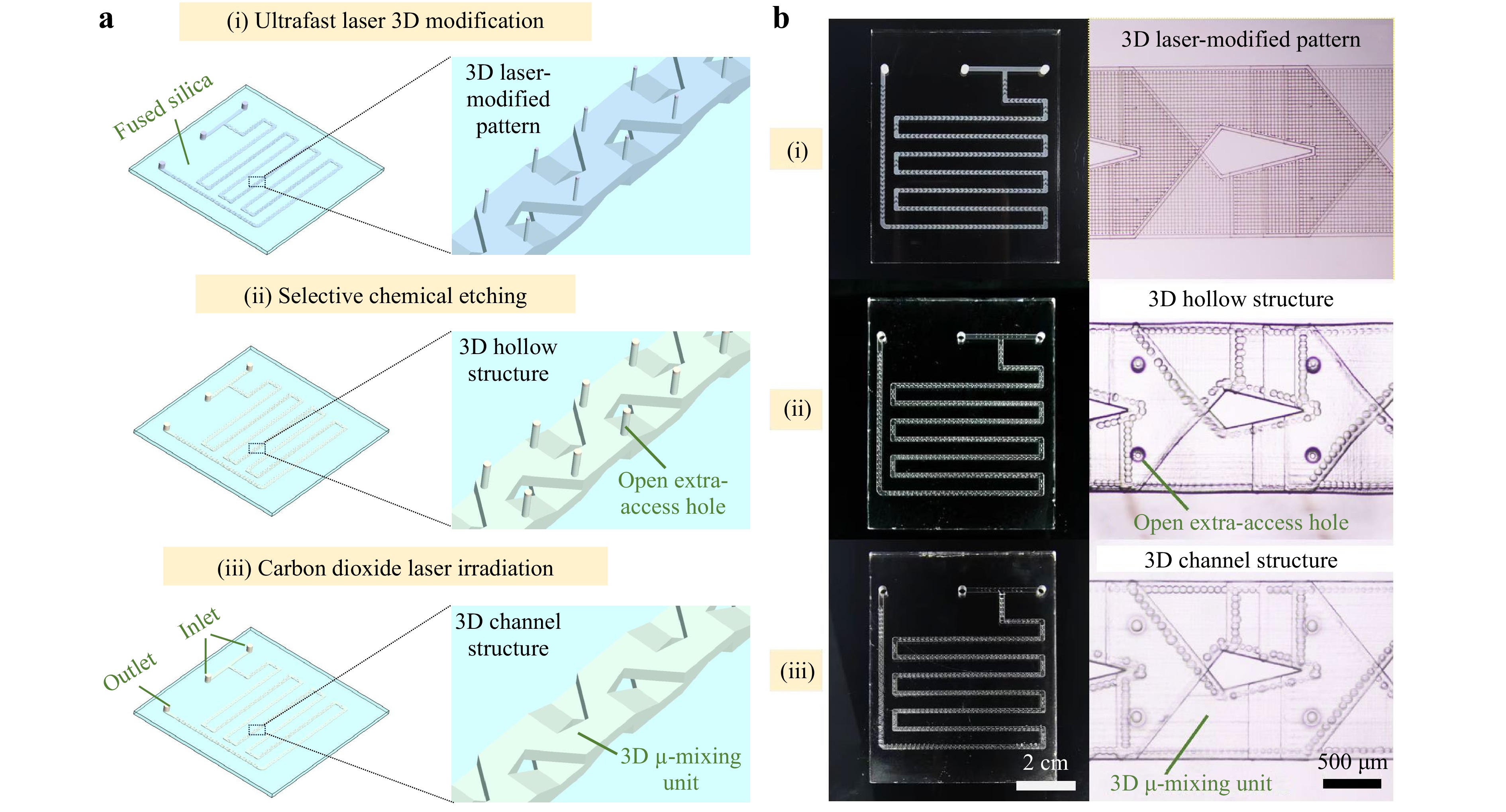
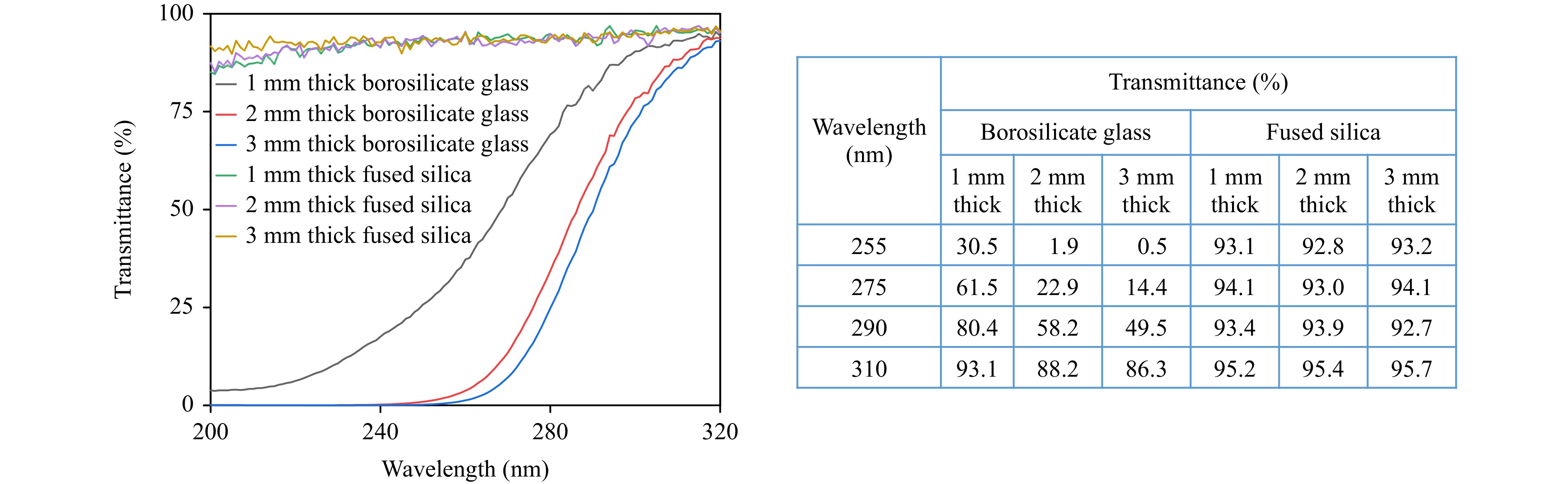
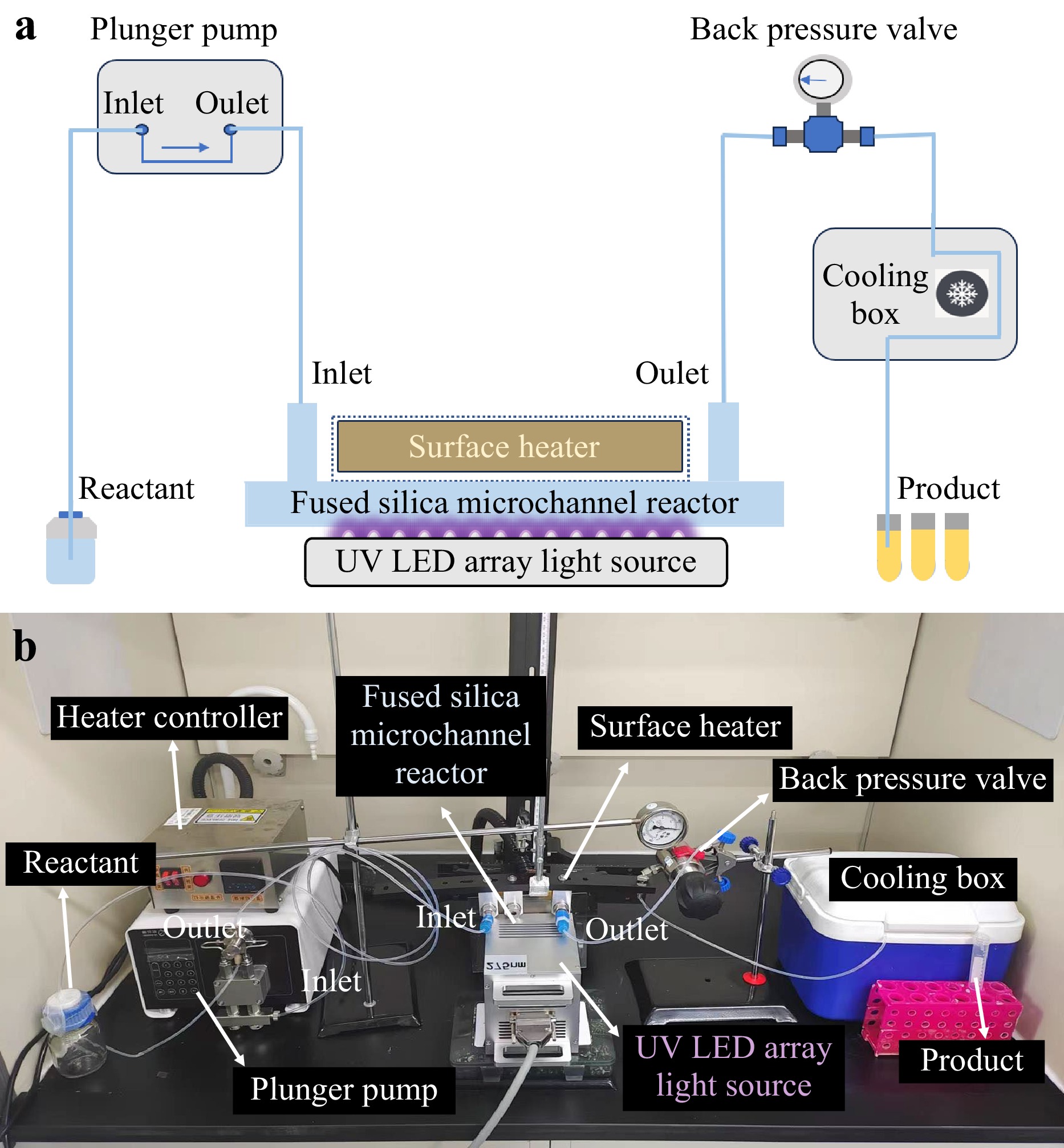
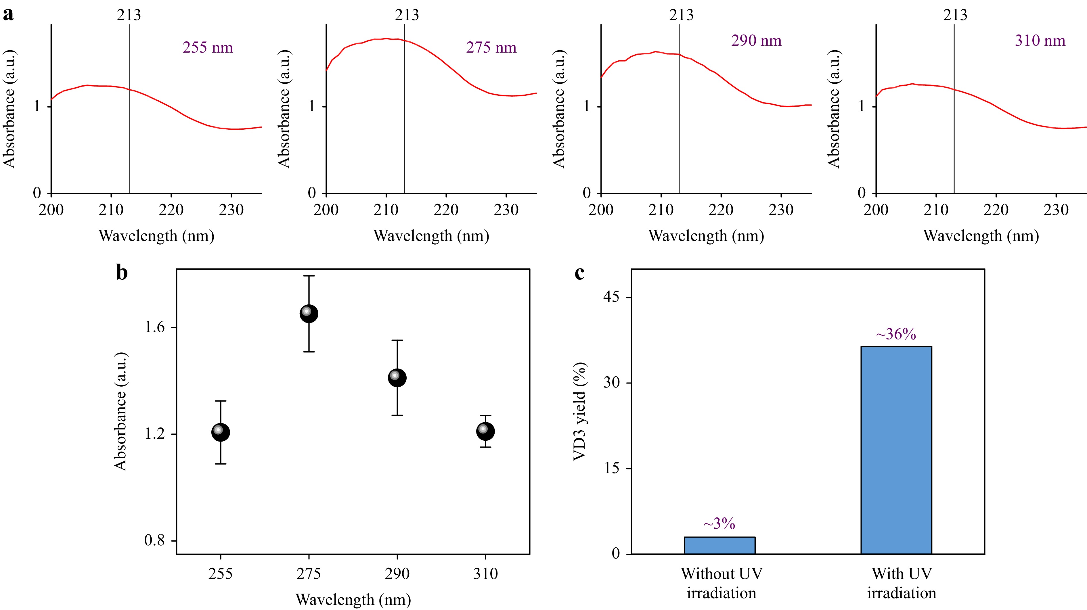
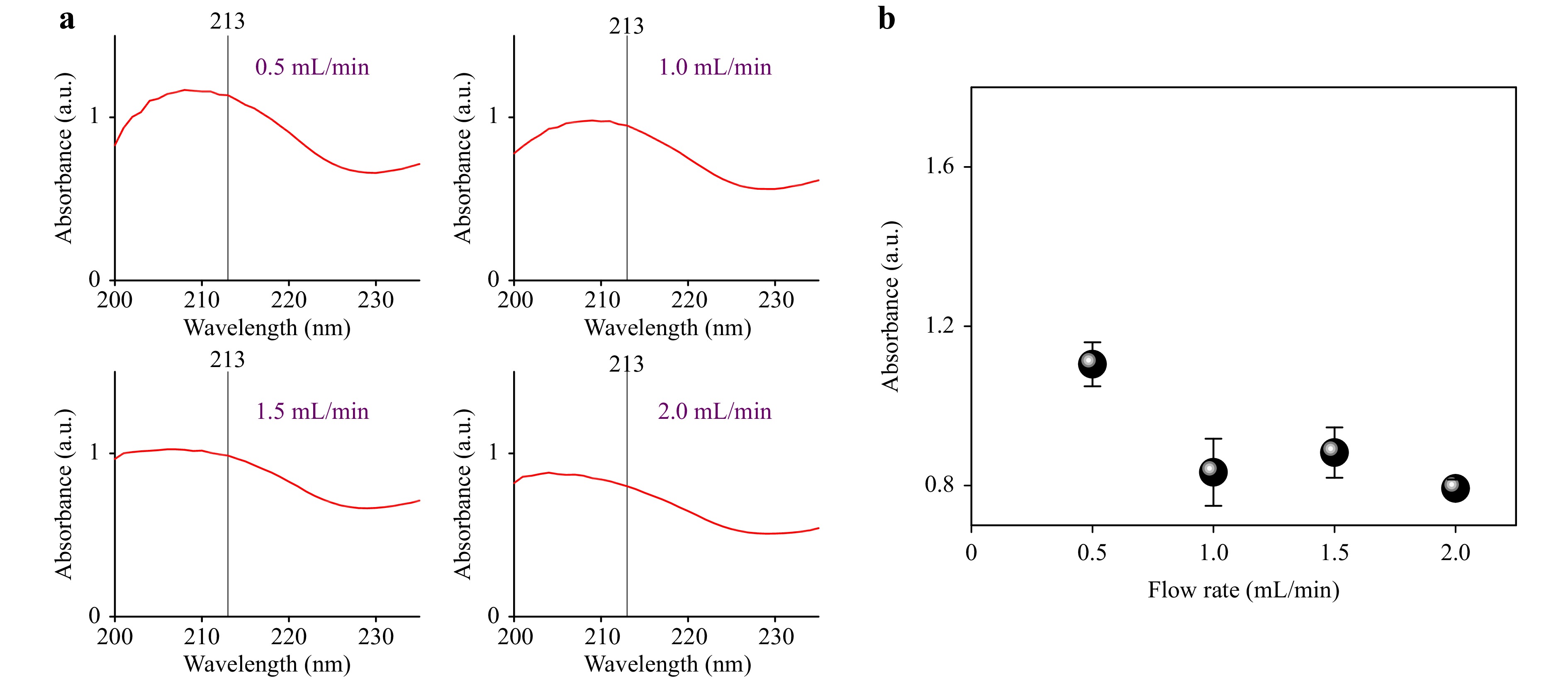
Large-scale, high-precision, and high-transparency microchannels hold great potential for developing high-performance continuous-flow photochemical reactions. We demonstrated ultrafast laser-enabled fabrication of three-dimensional microchannel reactors in ultraviolet (UV) grade fused silica which exhibit high transparency under the illumination of UV light sources of wavelengths well below 300 nm with excellent mixing efficiency. With the fabricated glass microchannel reactors, we demonstrated continuous-flow photochemical synthesis of vitamin D3 with UV LED array light sources.
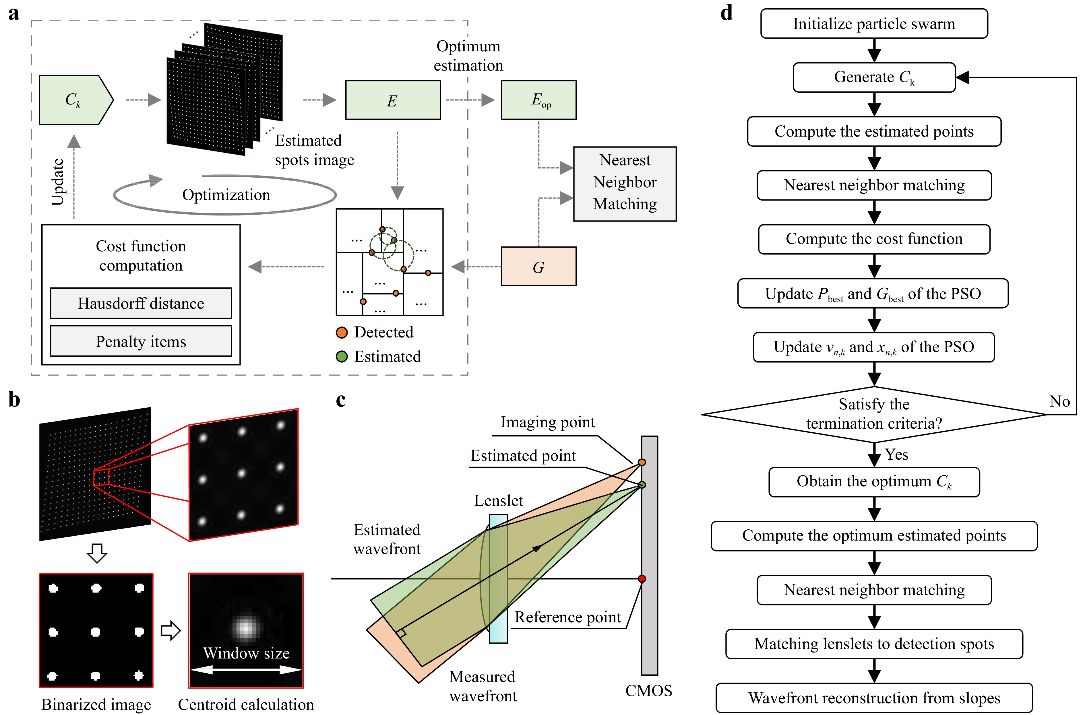
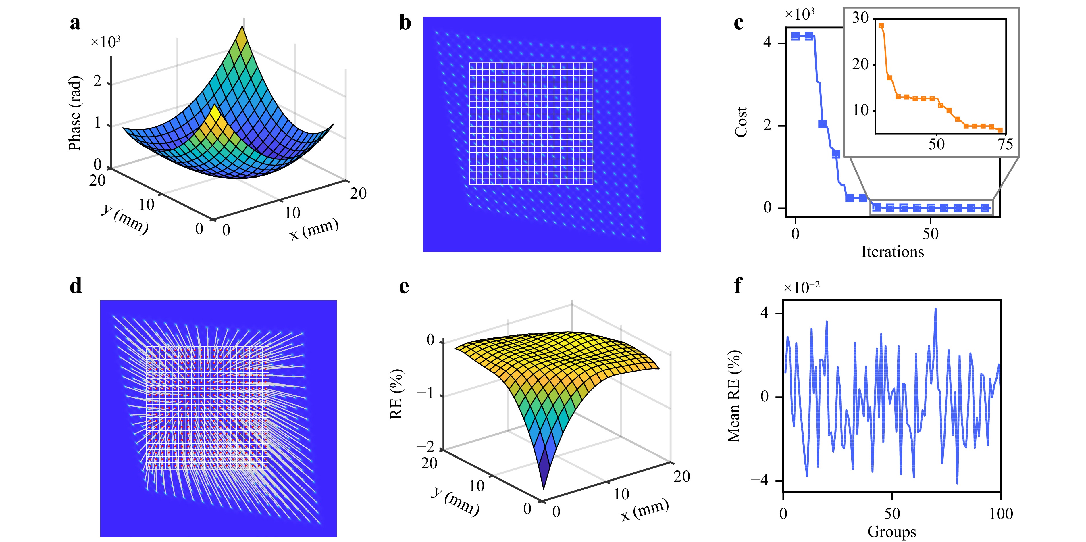
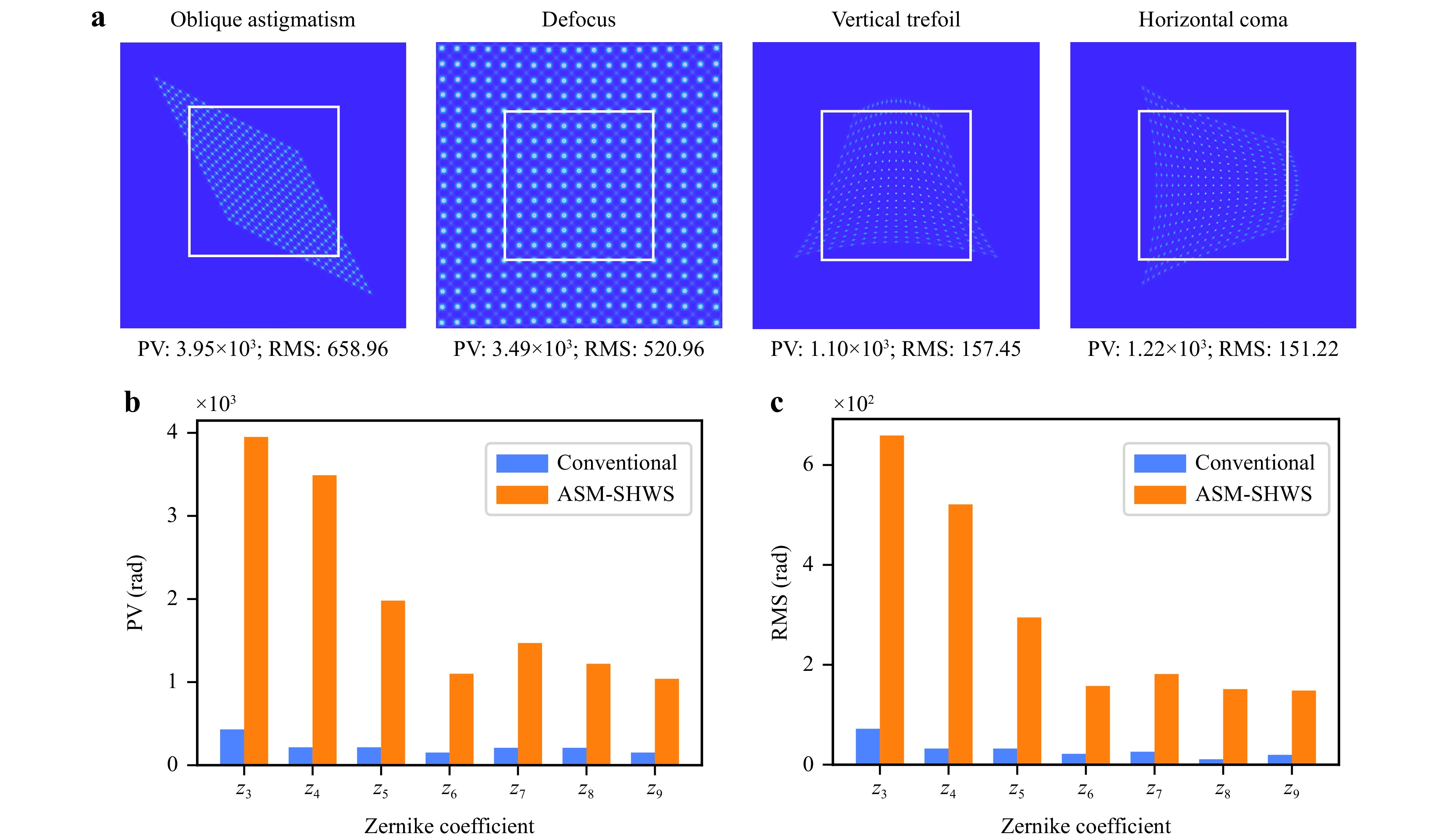
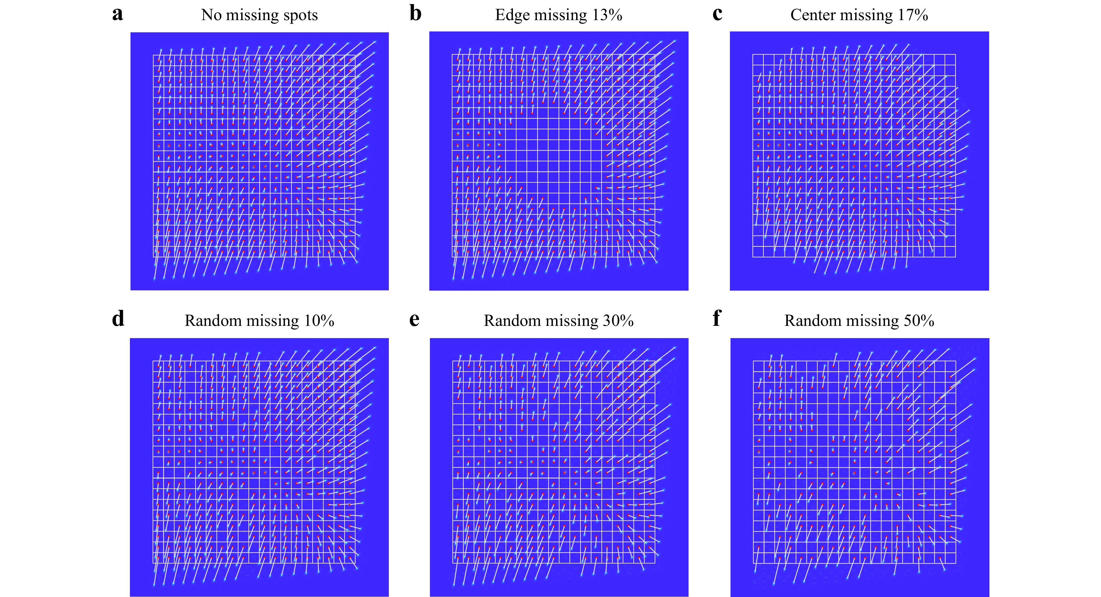
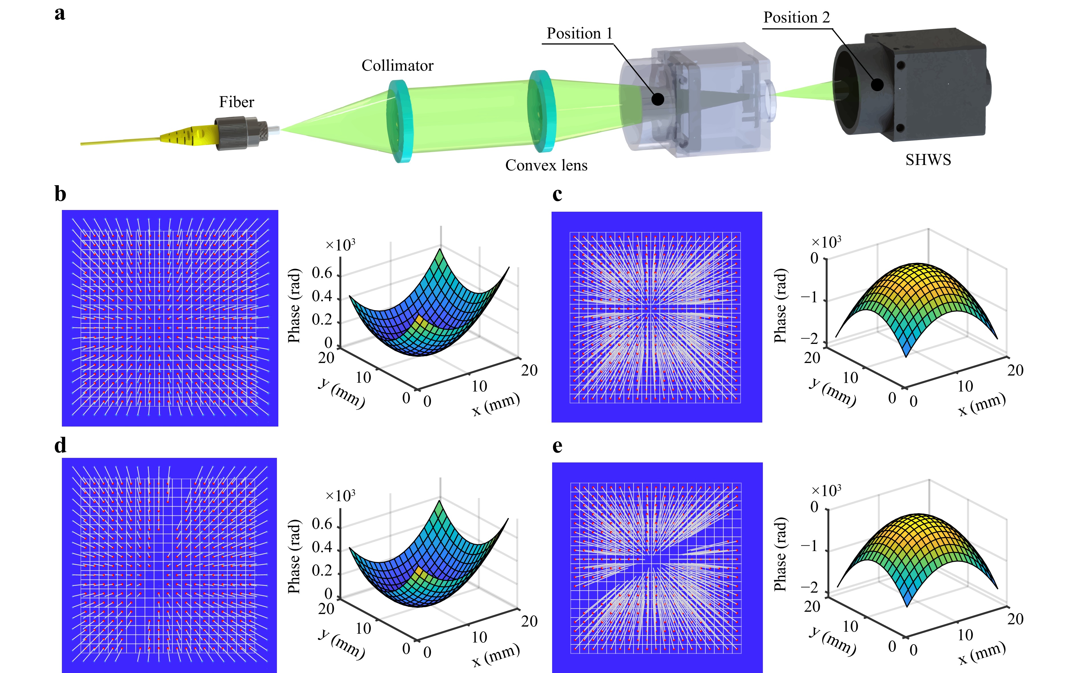
The Shack-Hartmann wavefront sensor (SHWS) is widely used for high-speed, precise, and stable wavefront measurements. However, conventional SHWSs encounter a limitation in that the focused spot from each microlens is restricted to a single microlens, leading to a limited dynamic range. Herein, we propose an adaptive spot matching (ASM)-based SHWS to extend the dynamic range. This approach involves seeking an incident wavefront that best matches the detected spot distribution by employing a Hausdorff-distance-based nearest-distance matching strategy. The ASM-SHWS enables comprehensive spot matching across the entire imaging plane without requiring initial spot correspondences. Furthermore, due to its global matching capability, ASM-SHWS can maintain its capacity even if a portion of the spots are missing. Experiments showed that the ASM-SHWS could measure a high-curvature spherical wavefront with a local slope of 204.97 mrad, despite a 12.5% absence of spots. This value exceeds that of the conventional SHWS by a factor of 14.81.
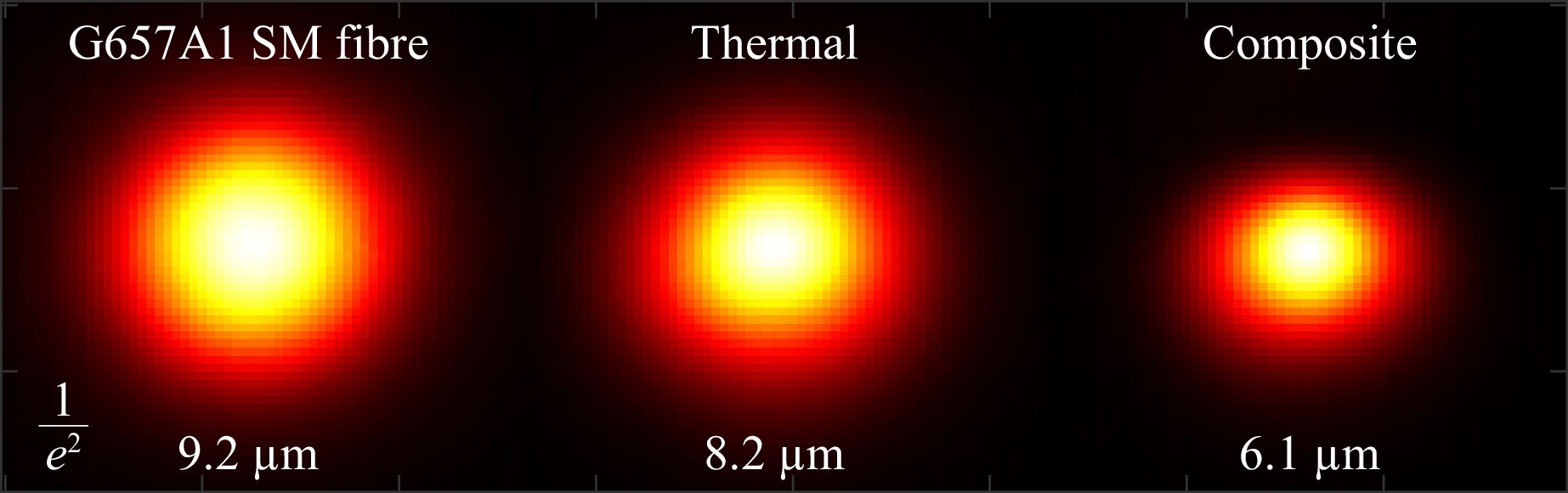
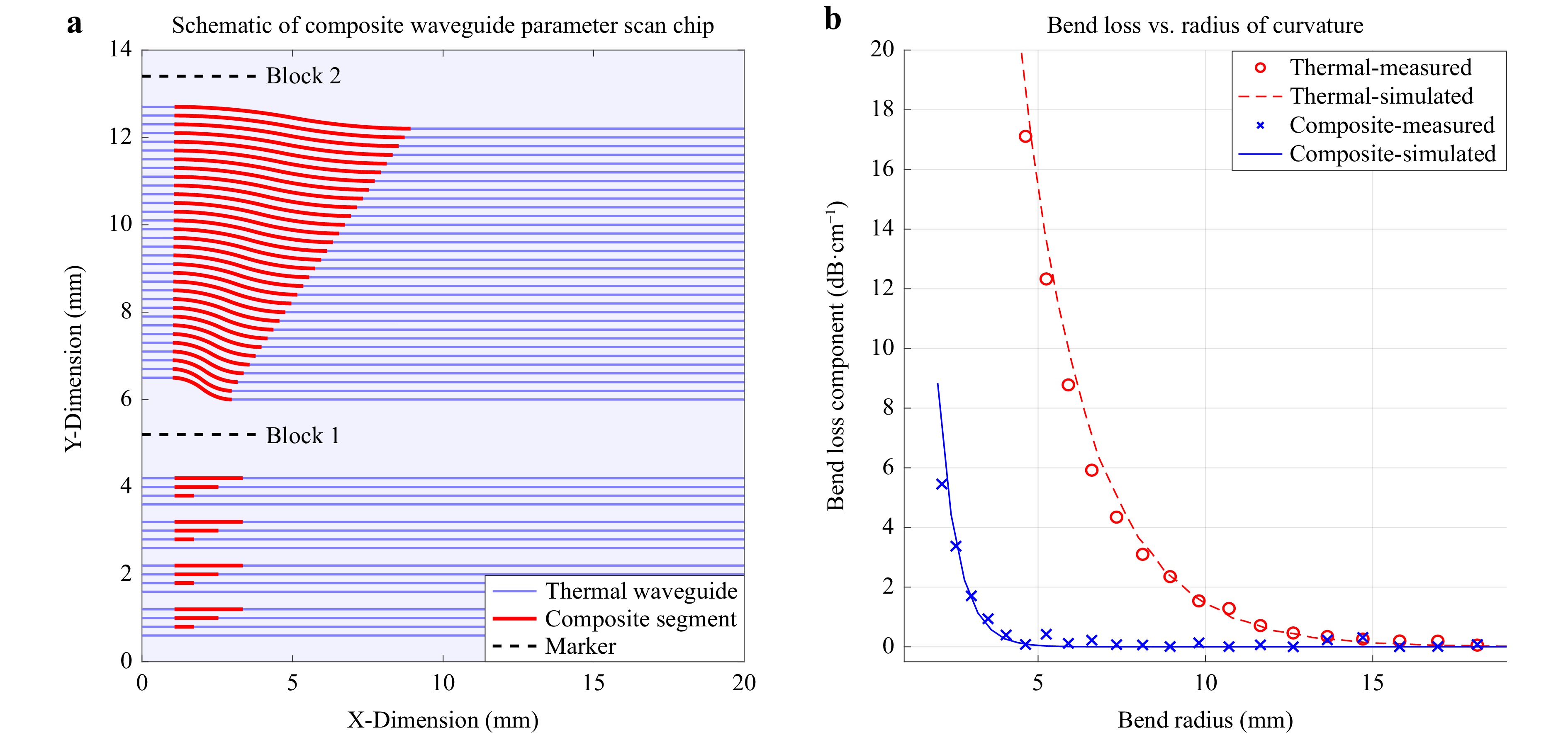
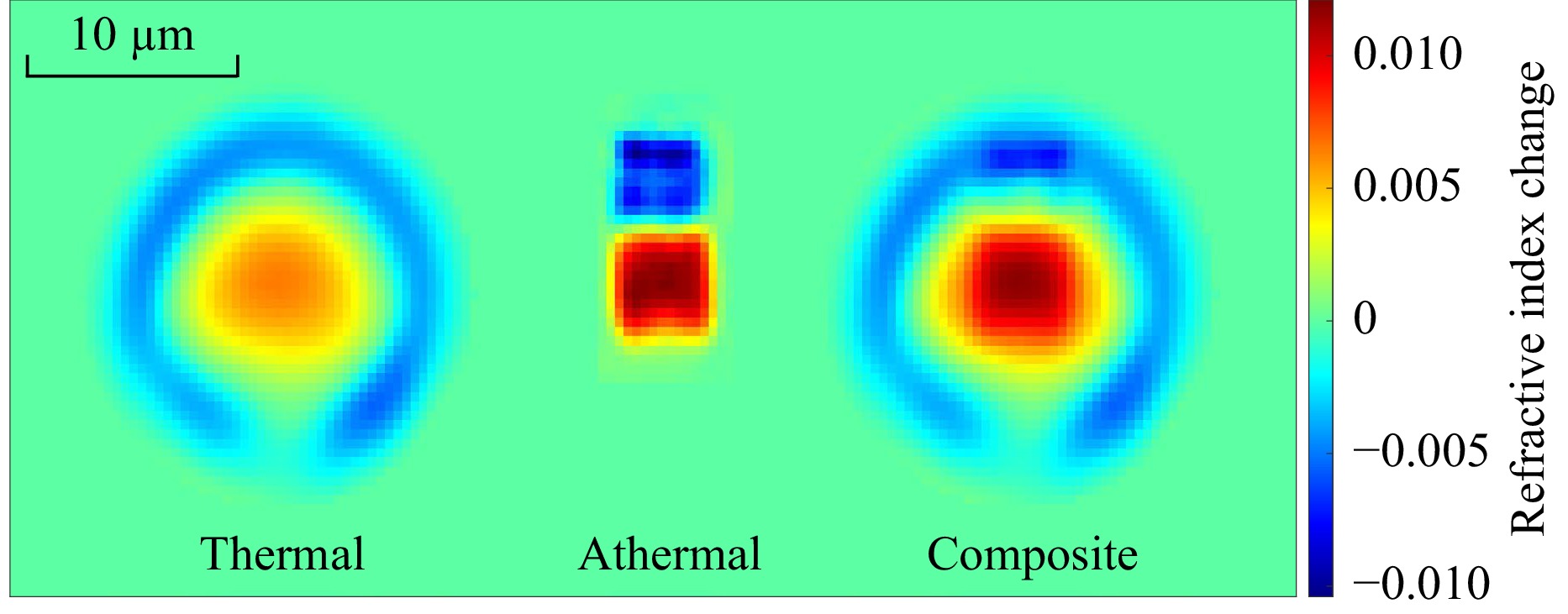
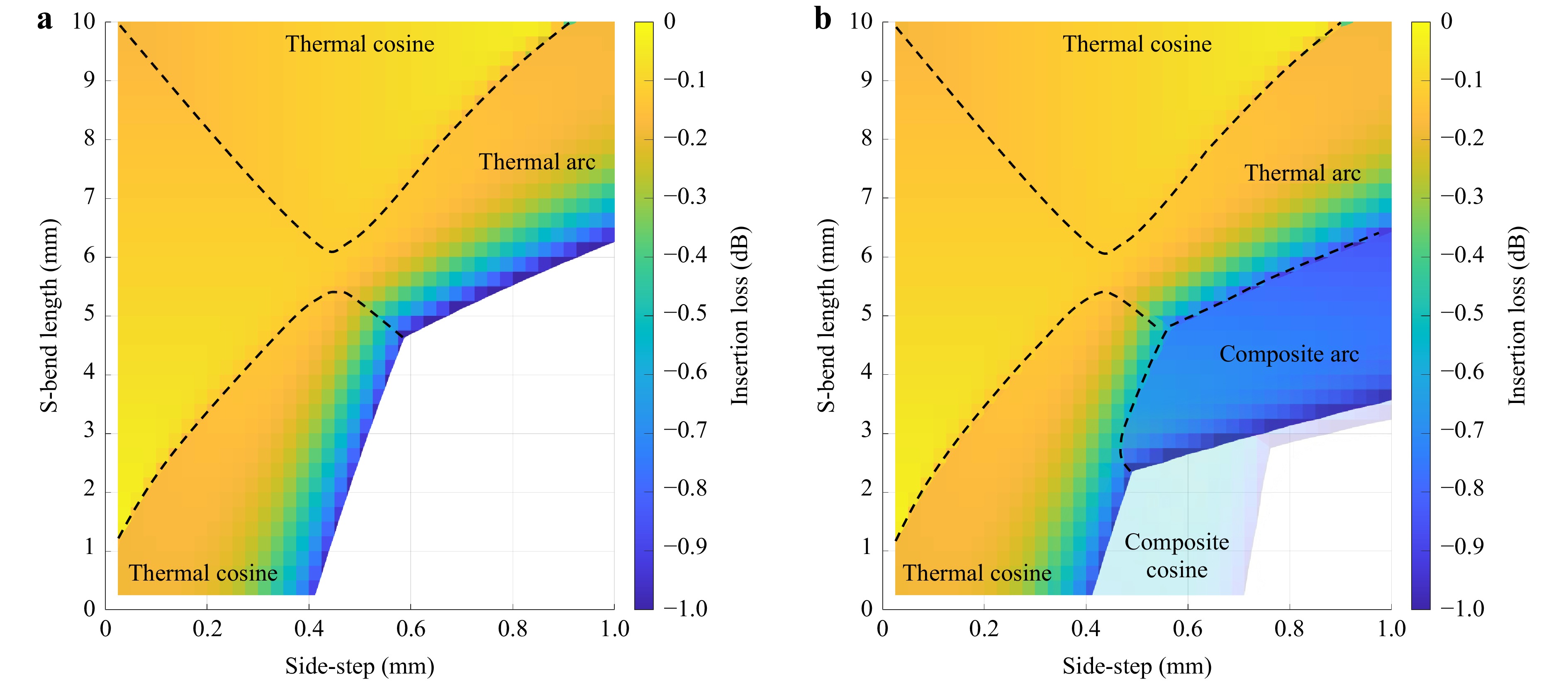
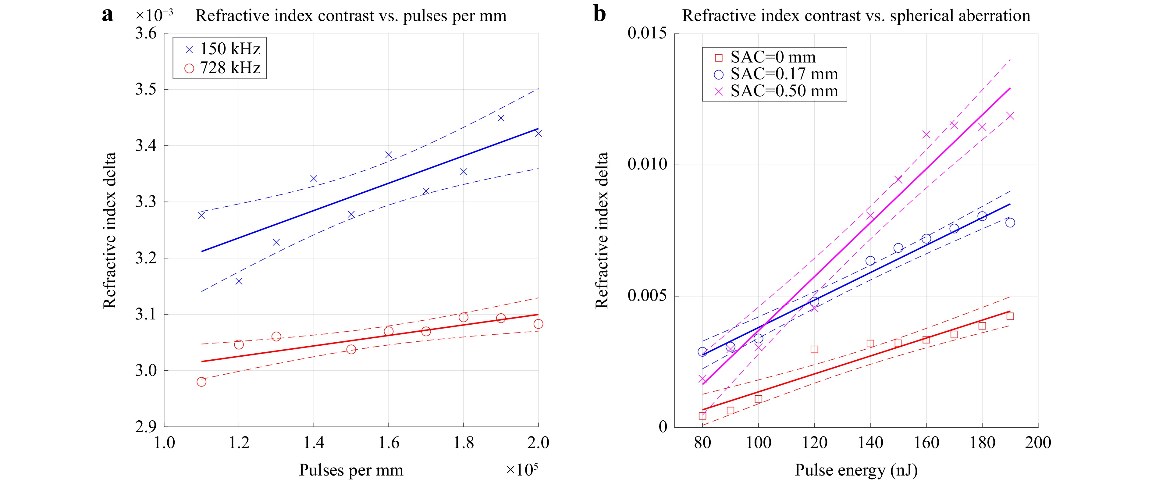
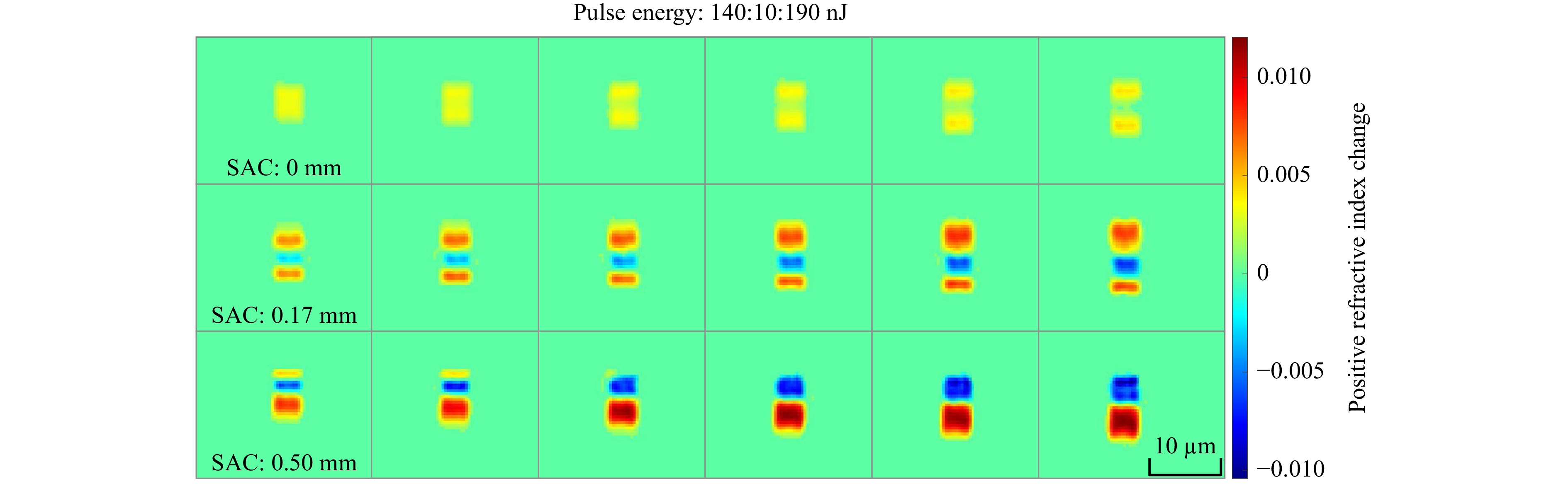
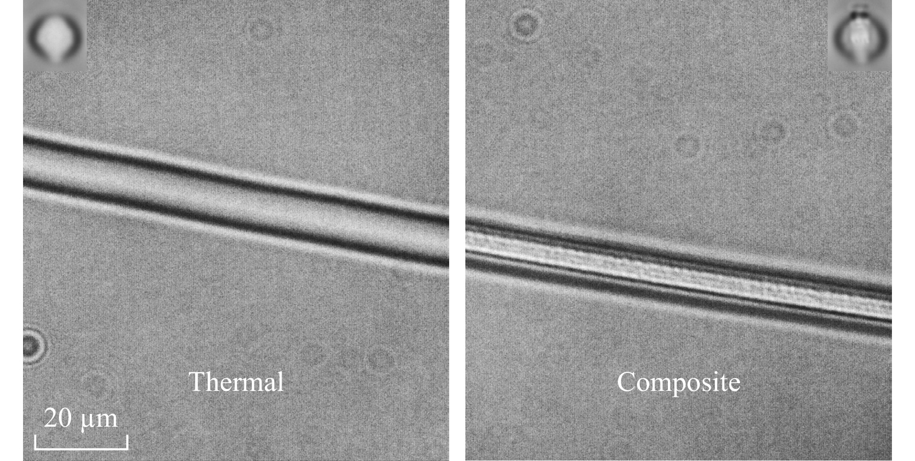
We demonstrate a novel, composite laser written 3D waveguide, fabricated in boro-aluminosilicate glass, with a refractive index contrast of 1.12 × 10⁻². The waveguide is fabricated using a multi-pass approach which leverages the respective refractive index modification mechanisms of both the thermal and athermal inscription regimes. We present the study and optimisation of inscription parameters for maximising positive refractive index change and ultimately demonstrate a dramatic advancement on the state of the art of bend losses in laser-written waveguides. The 1.0 dB cm−1 bend loss cut-off radius is reduced from 10 mm to 4 mm, at a propagation wavelength of 1550 nm.
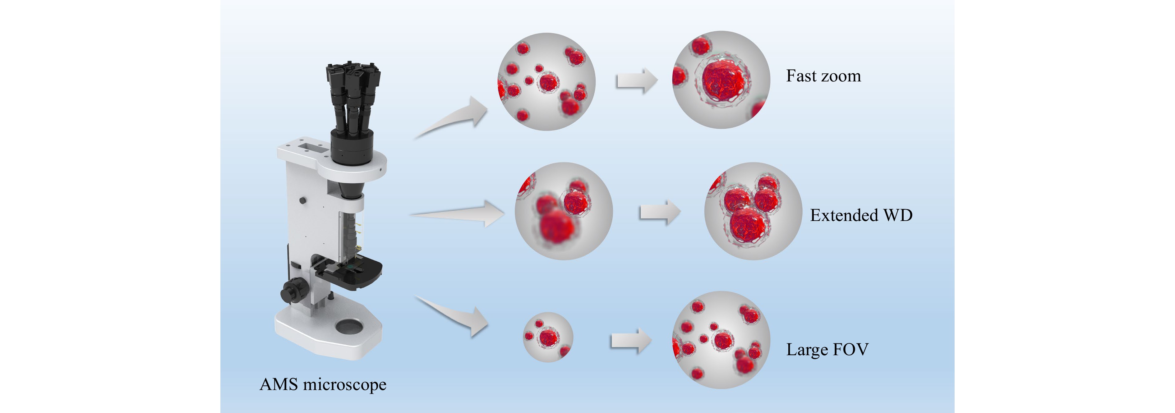
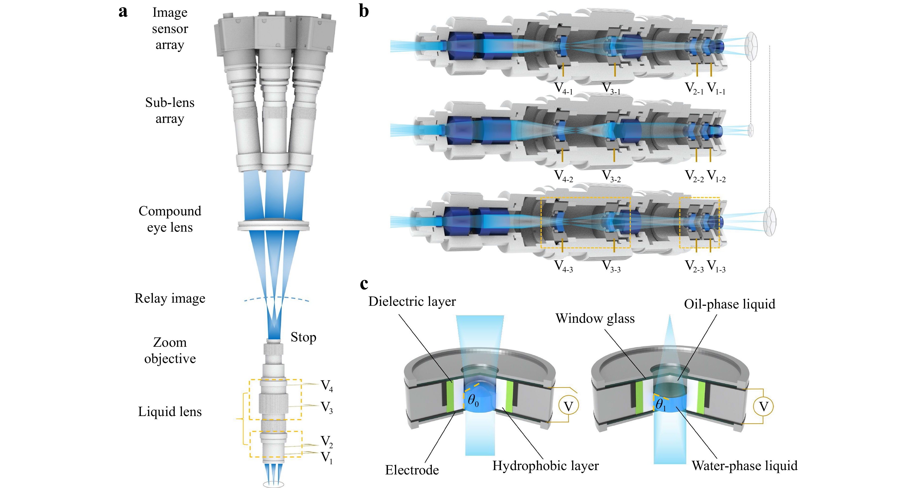
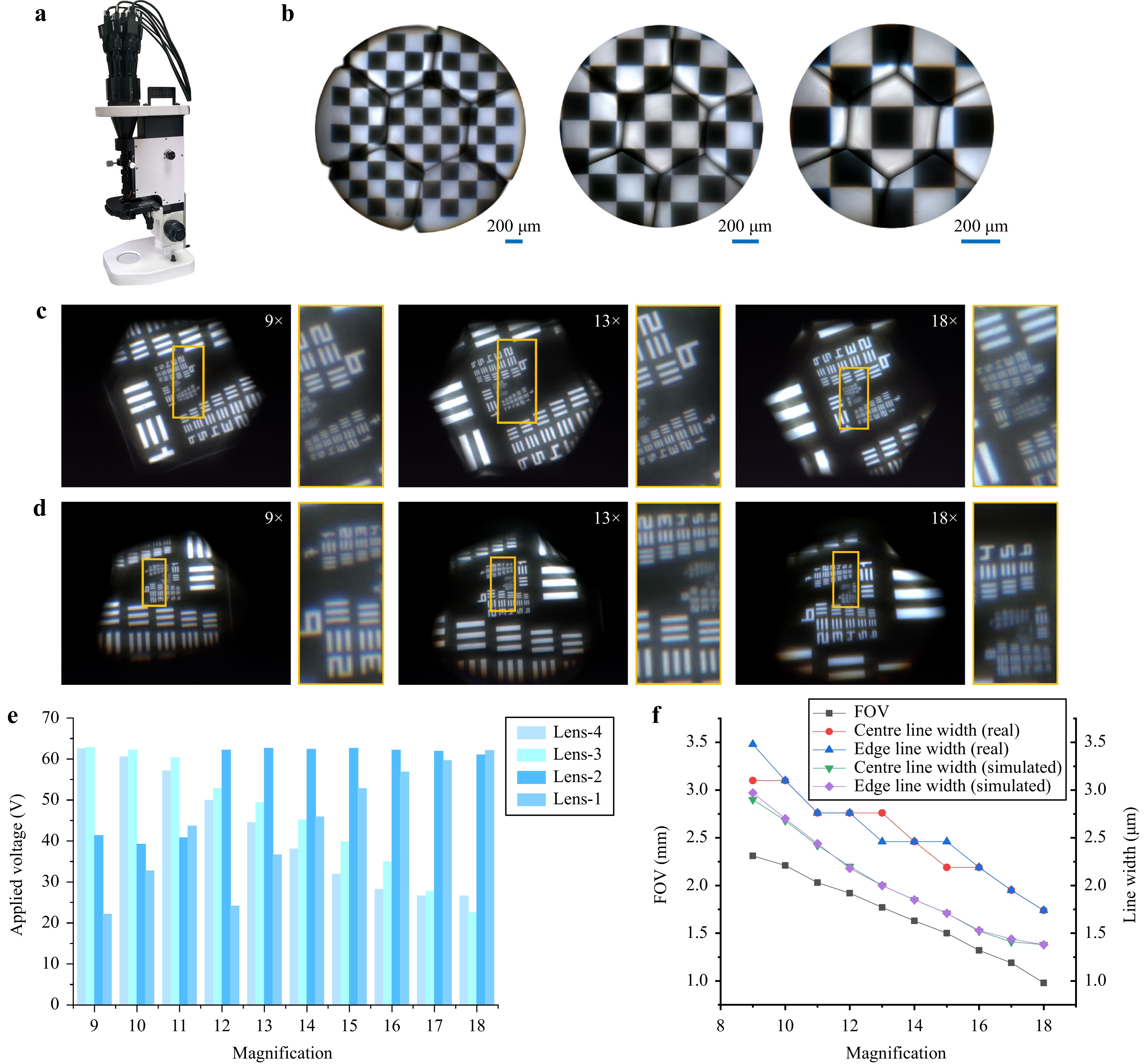
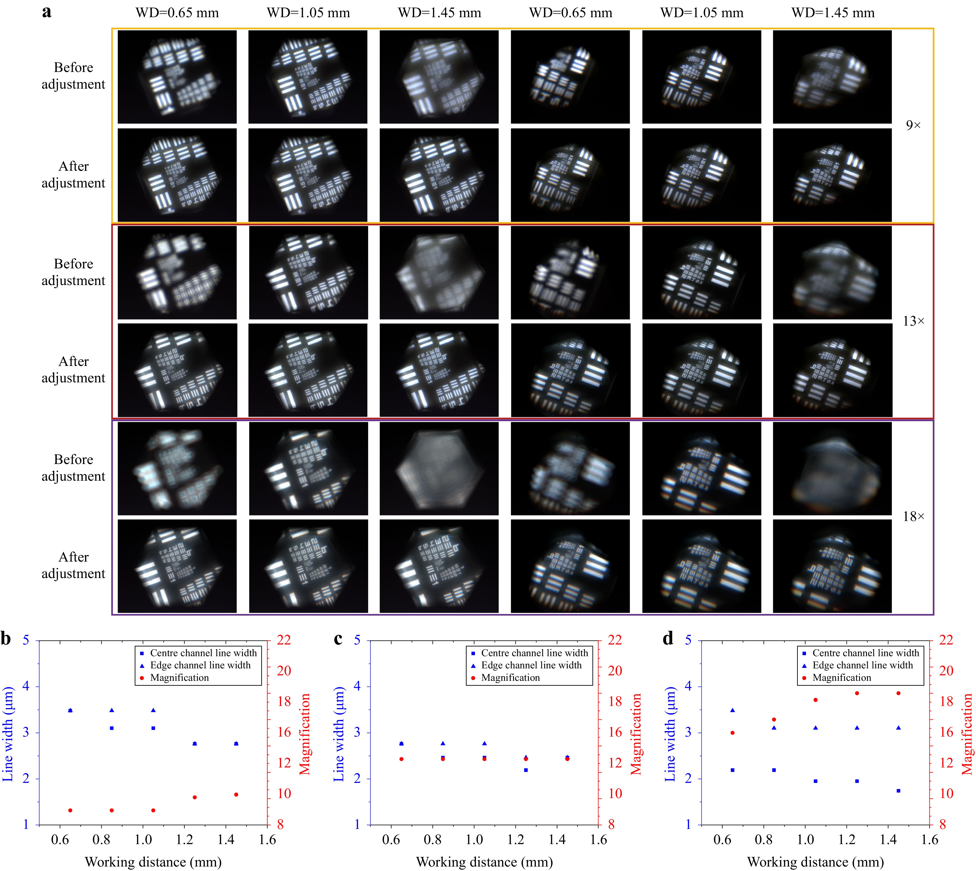
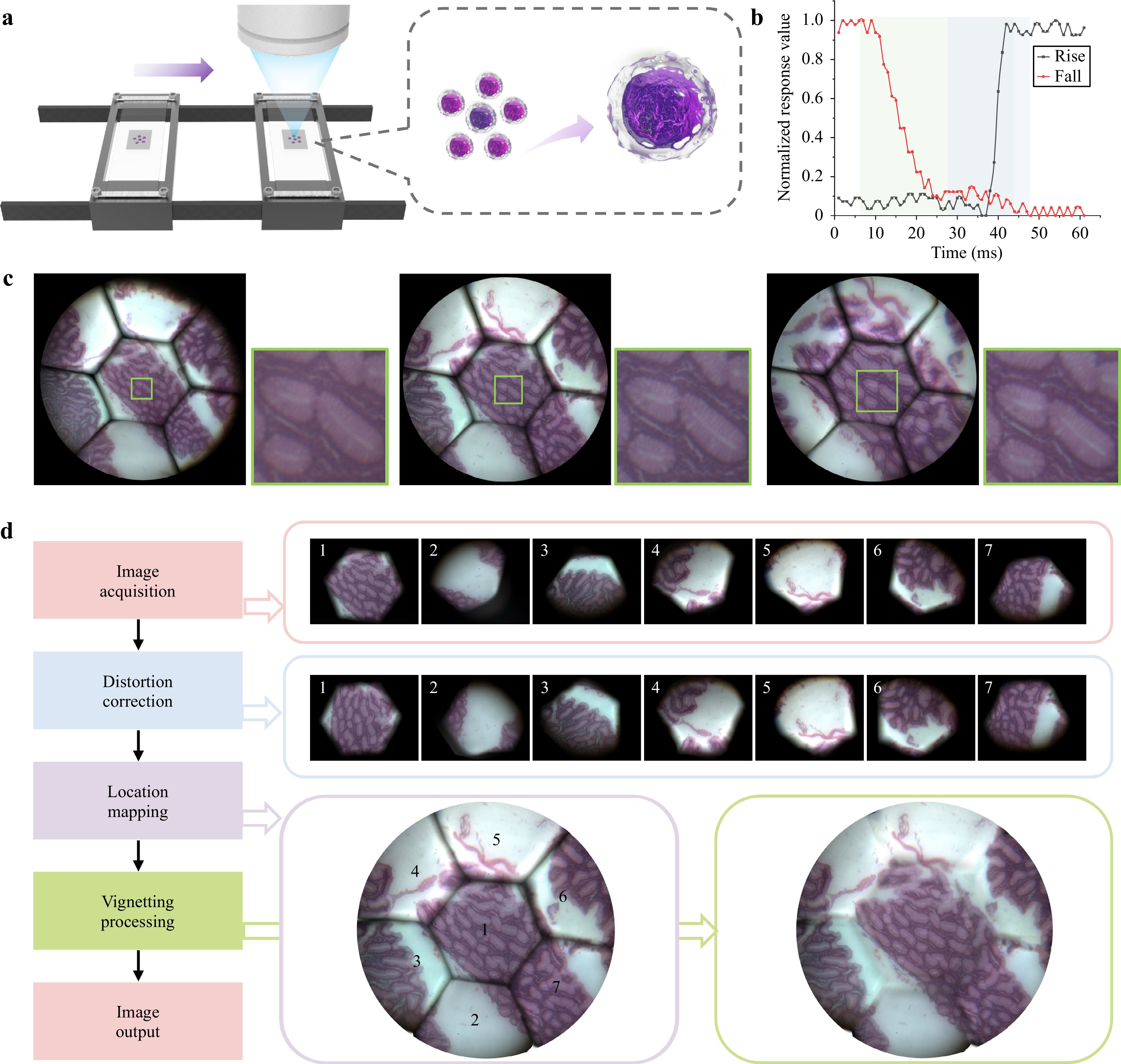
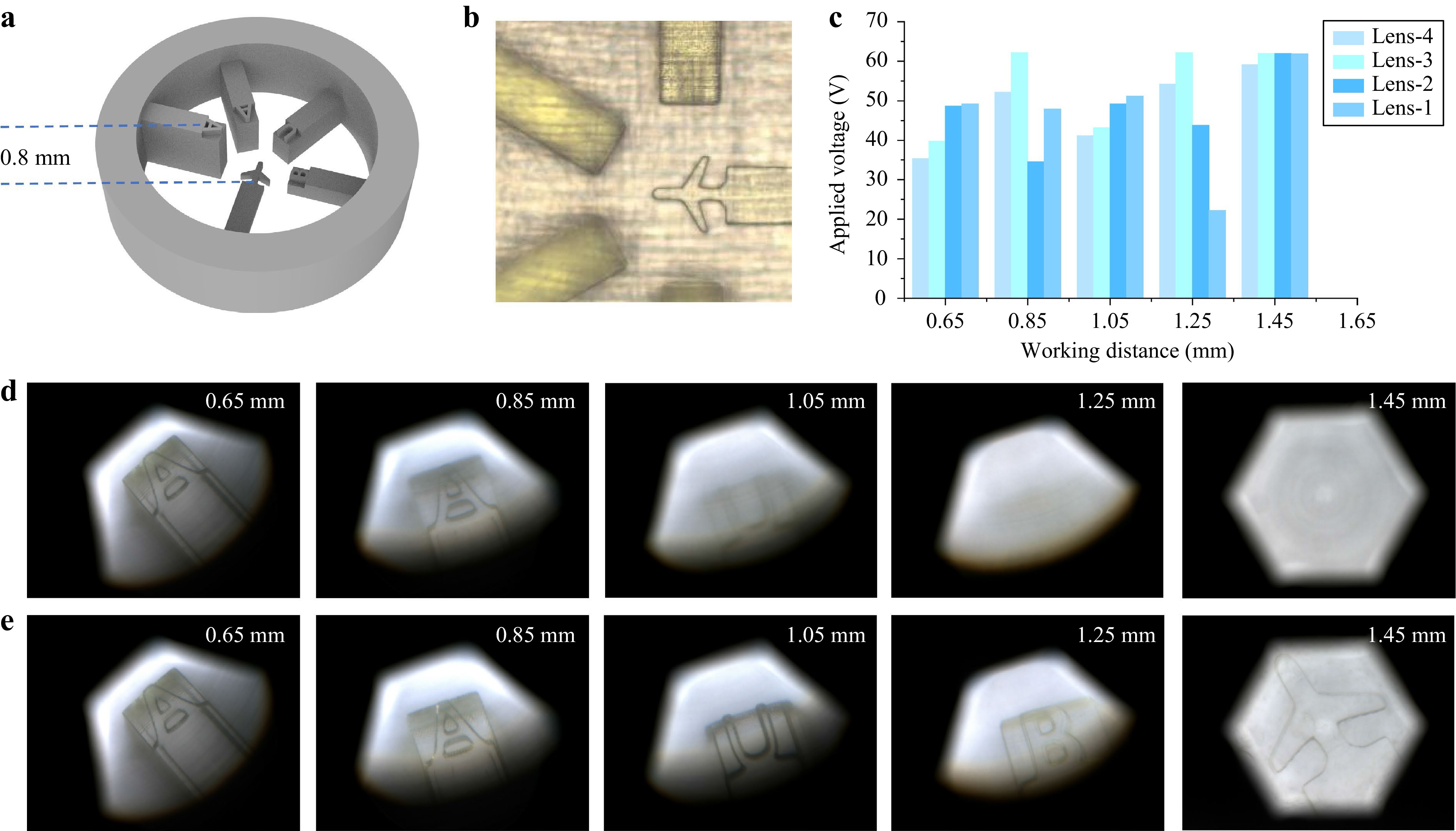
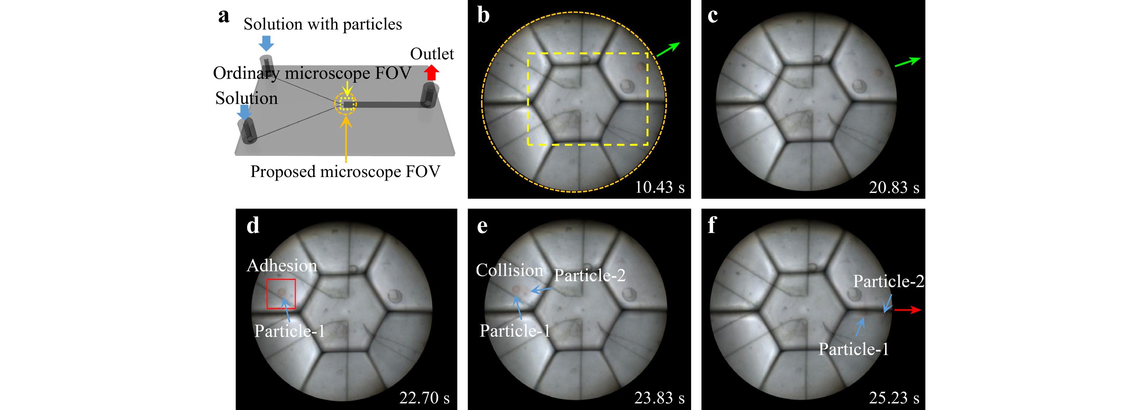
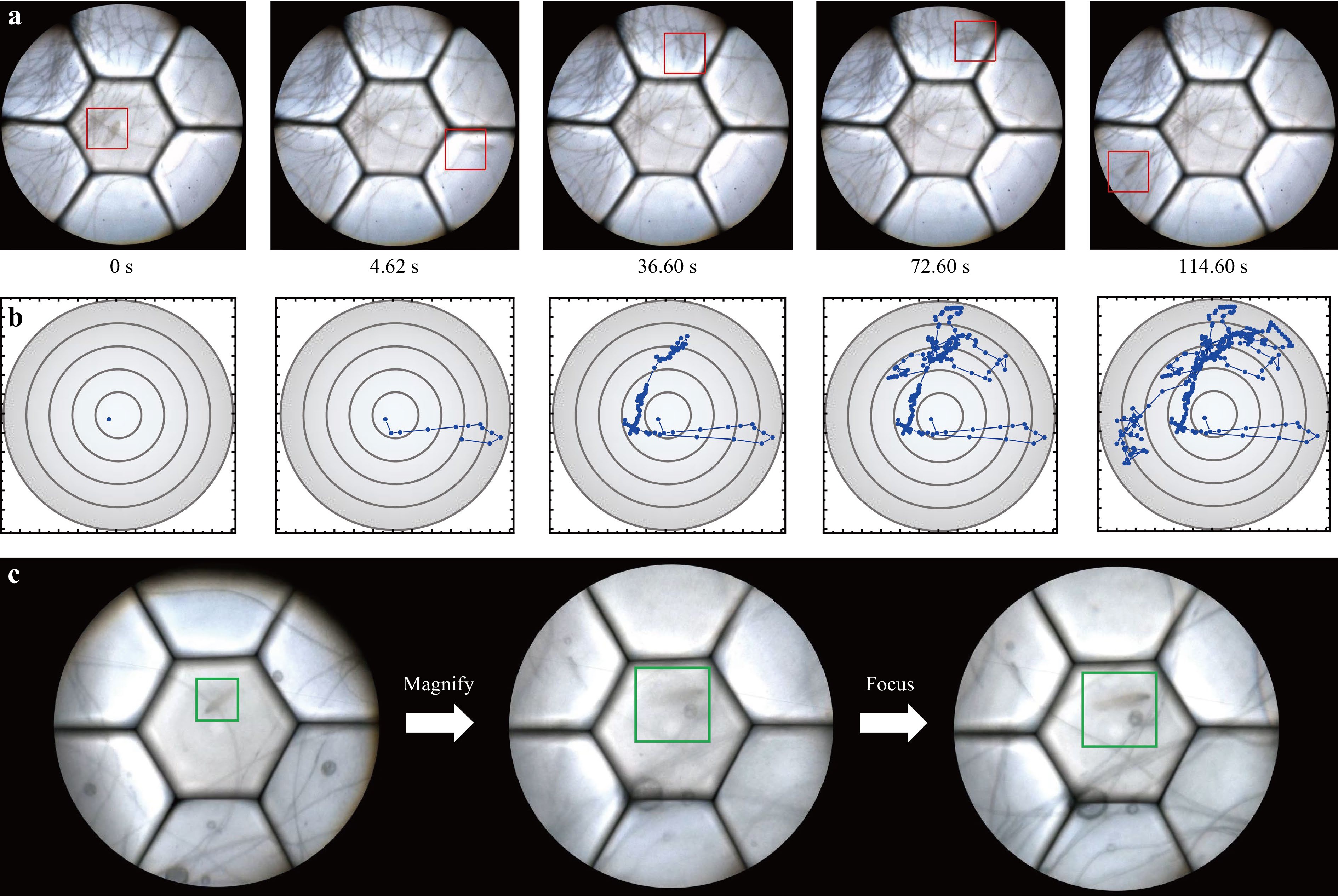
The field-of-view (FOV), depth of field, and resolution of conventional microscopes are constrained by each other; therefore, a zoom function is required. Traditional zoom methods lose real-time performance and have limited information throughput, severely limiting their application, especially in three-dimensional dynamic imaging and large-amount or large-size sample scanning. Here, an adaptive multiscale (AMS) imaging mechanism combining the benefits of liquid lenses and multiscale imaging techniques is proposed to realize the functions of fast zooming, wide working distance (WD) range and large FOV on a self-developed AMS microscope. The design principles were revealed. Moreover, a nonuniform-distortion-correction algorithm and a composite patching algorithm were designed to improve image quality. The continuous tunable magnification range of the AMS microscope is from 9× to 18×, with the corresponding FOV diameters and resolution ranging from 2.31 to 0.98 mm and from 161 to 287 line-pairs/mm, respectively. The extended WD range is 0.8 mm and the zoom response time is 38 ms. Experiments demonstrated the advantages of the proposed microscope in pathological sample scanning, thick-sample imaging, microfluidic process monitoring, and the observation of living microorganisms. The proposed microscope is the first step towards zoom multiscale imaging technology and is expected to be applied in life sciences, medical diagnosis, and industrial detection.
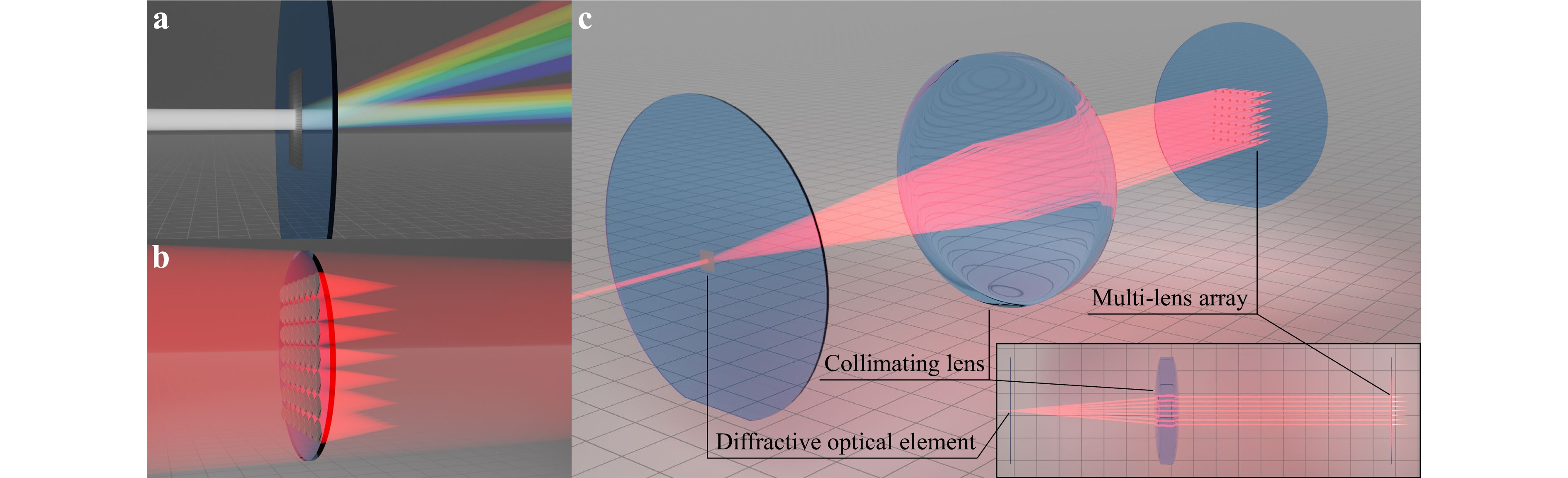
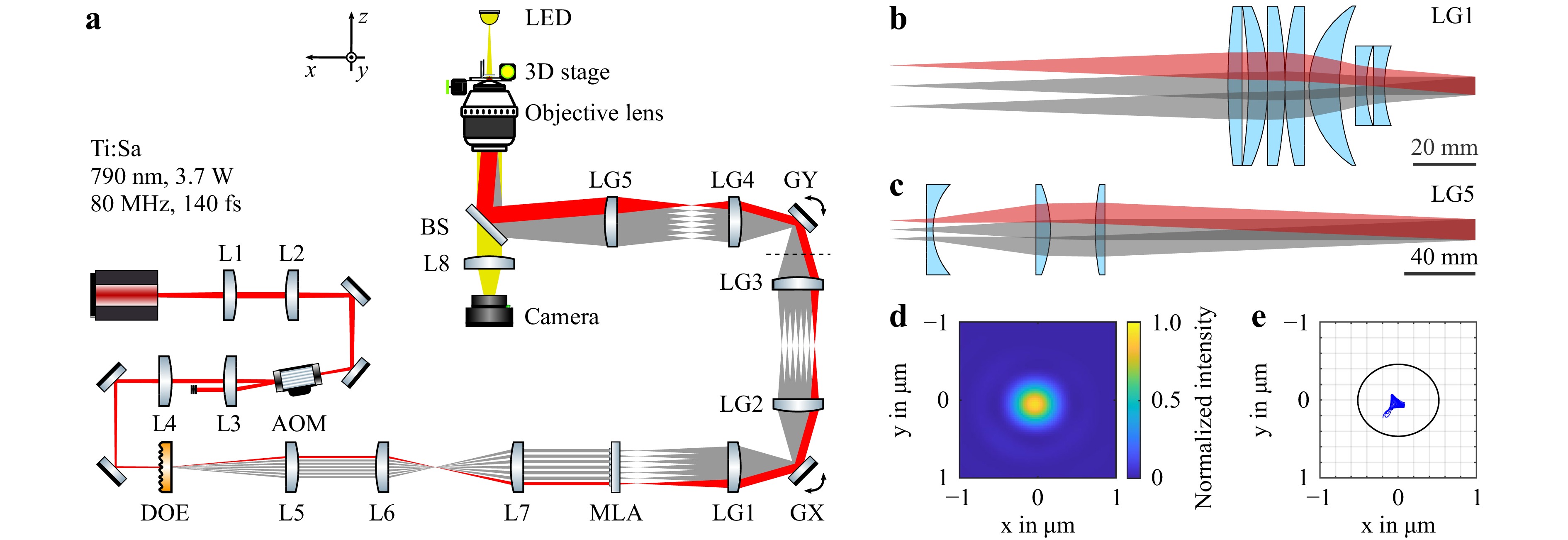
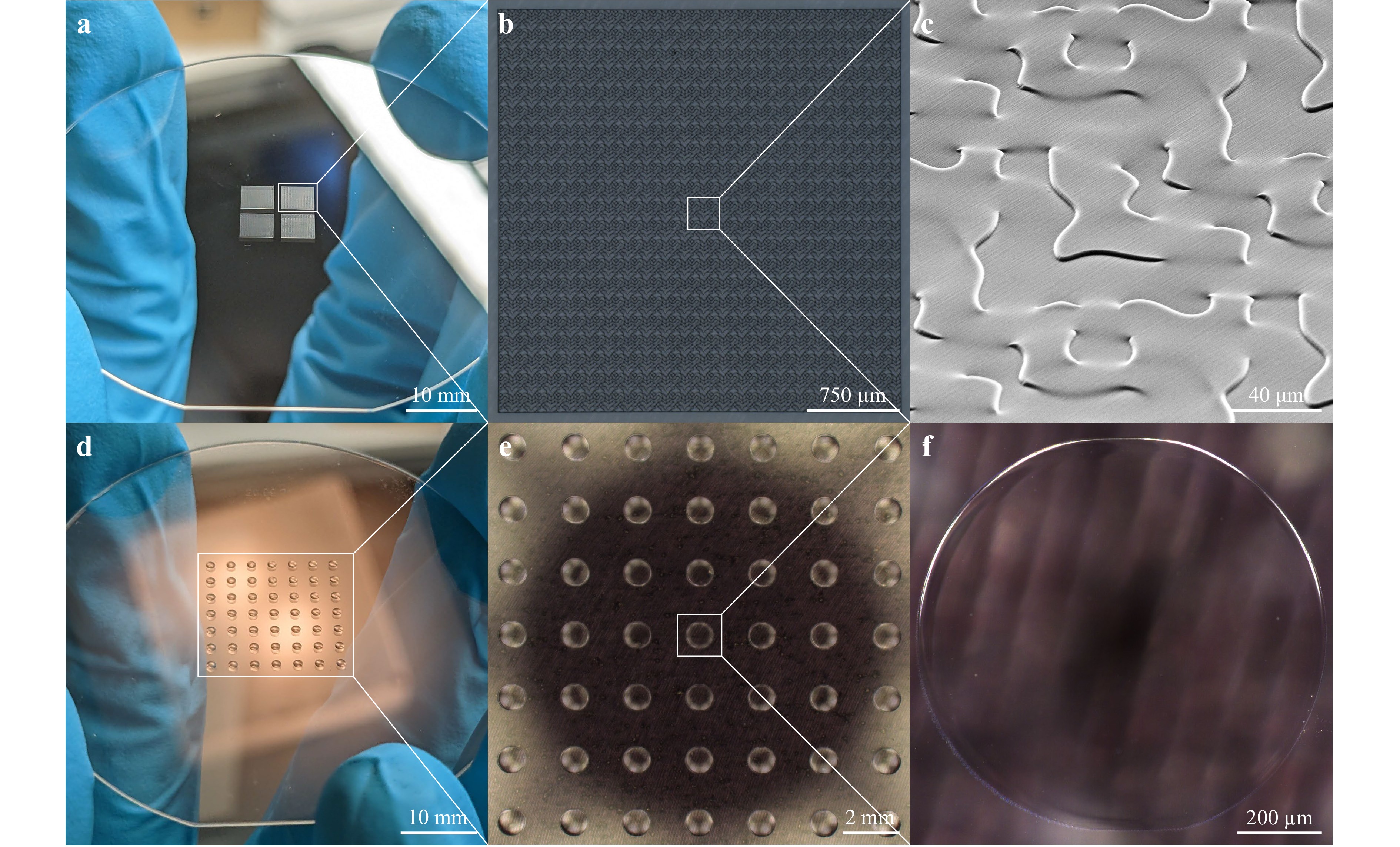
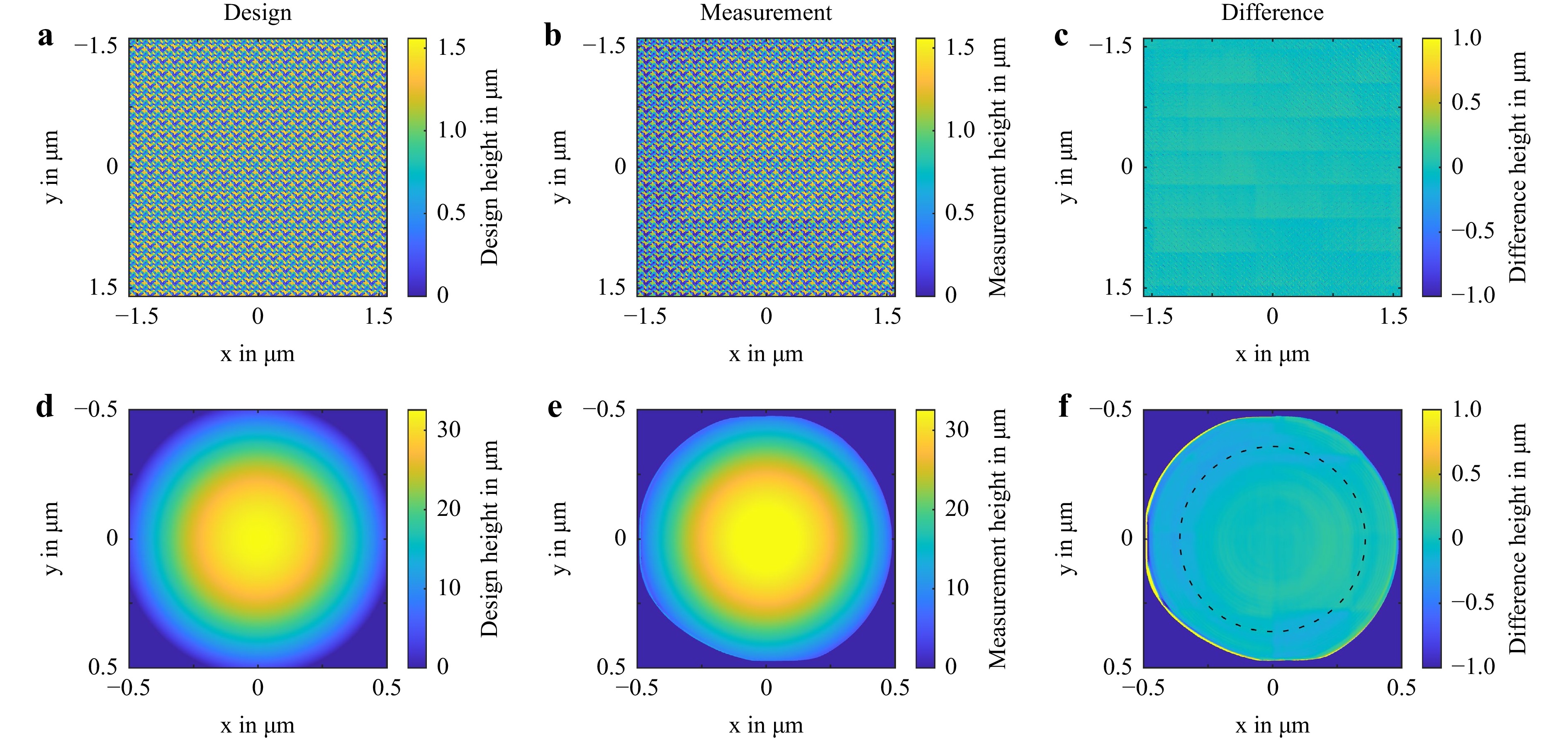
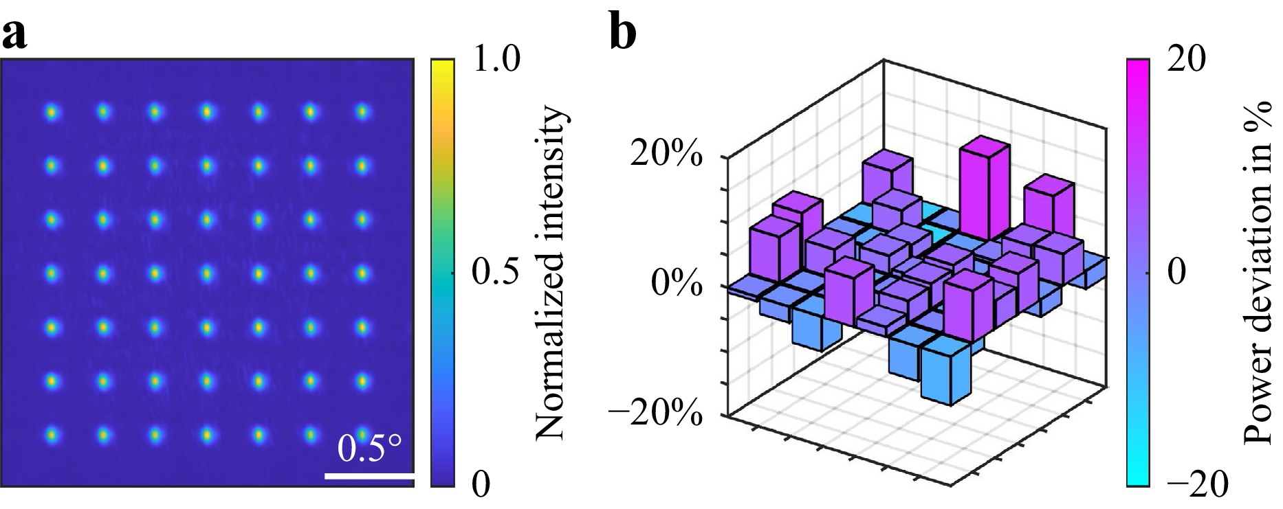
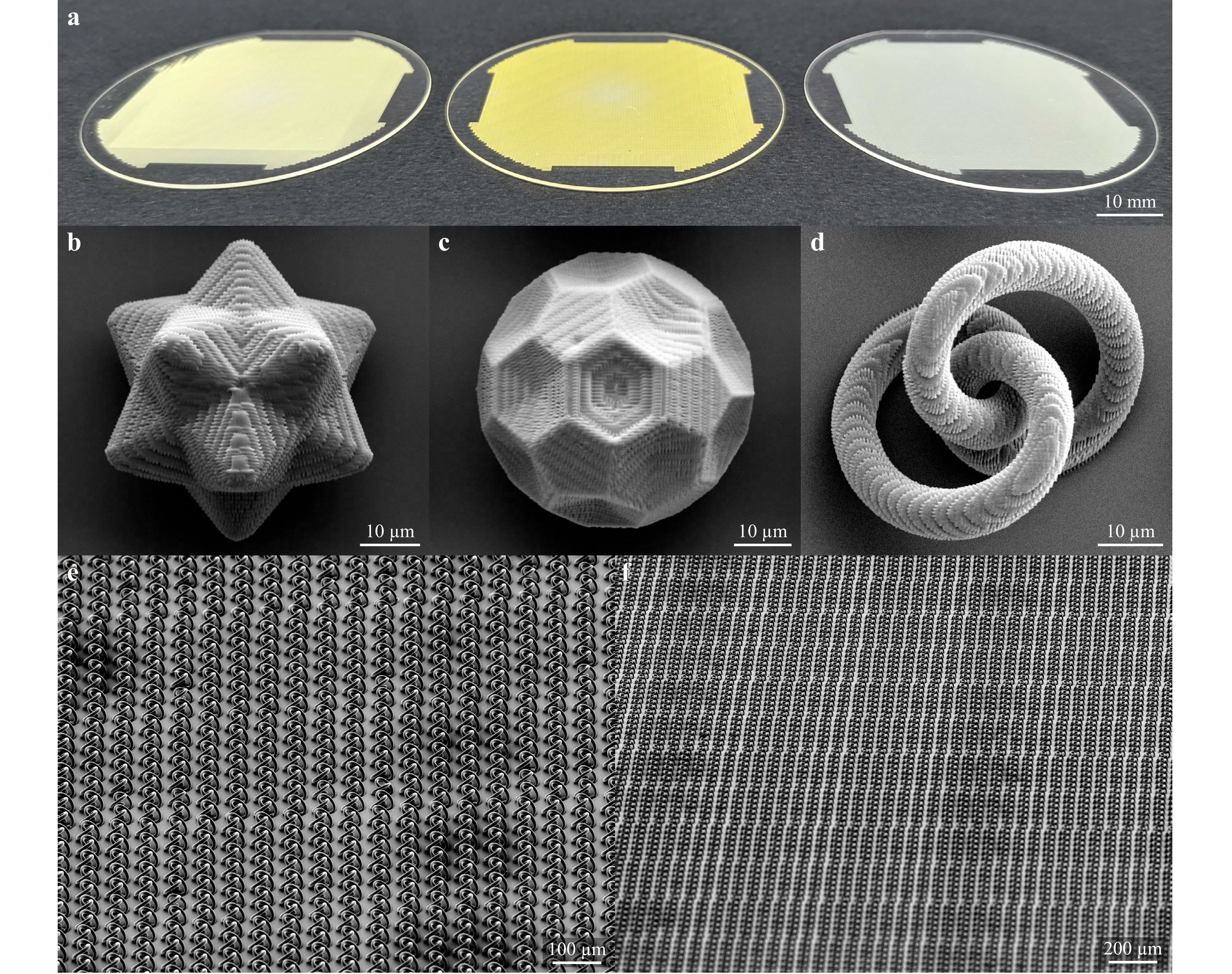
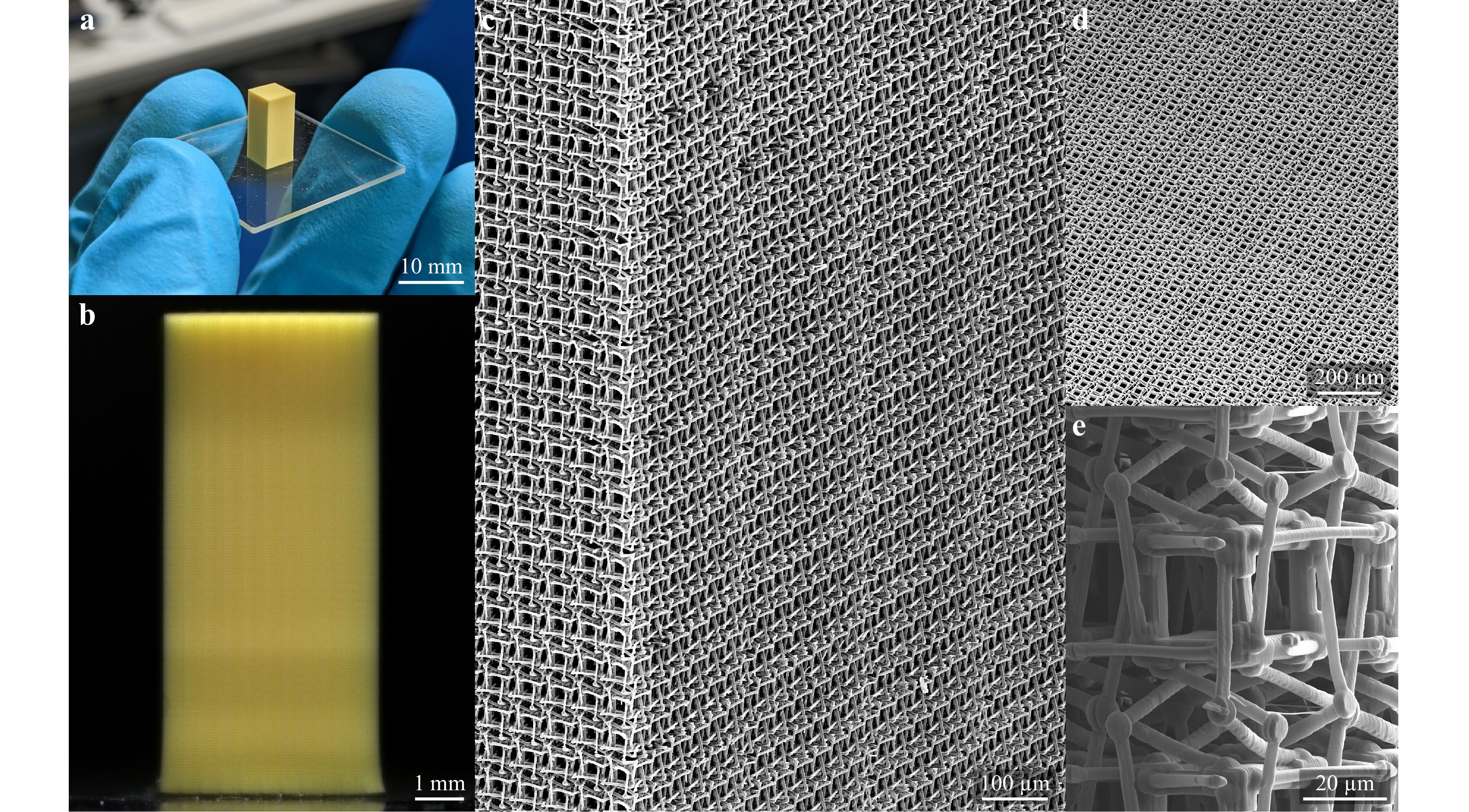
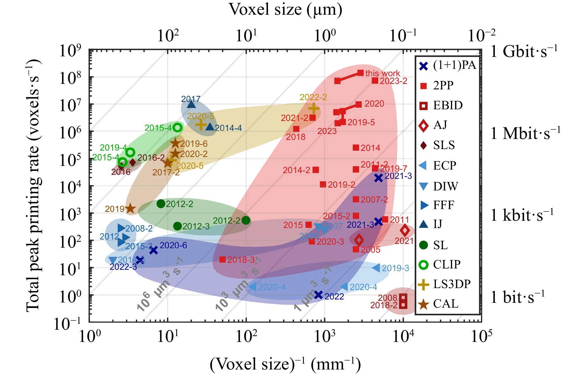
One of the challenges in the field of multi-photon 3D laser printing lies in further increasing the print speed in terms of voxels/s. Here, we present a setup based on a 7 × 7 focus array (rather than 3 × 3 in our previous work) and using a focus velocity of about 1 m/s (rather than 0.5 m/s in our previous work) at the diffraction limit (40×/NA1.4 microscope objective lens). Combined, this advance leads to a ten times increased print speed of about 108 voxels/s. We demonstrate polymer printing of a chiral metamaterial containing more than 1.7 × 10¹² voxels as well as millions of printed microparticles for potential pharmaceutical applications. The critical high-quality micro-optical components of the setup, namely a diffractive optical element generating the 7 × 7 beamlets and a 7 × 7 lens array, are manufactured by using a commercial two-photon grayscale 3D laser printer.
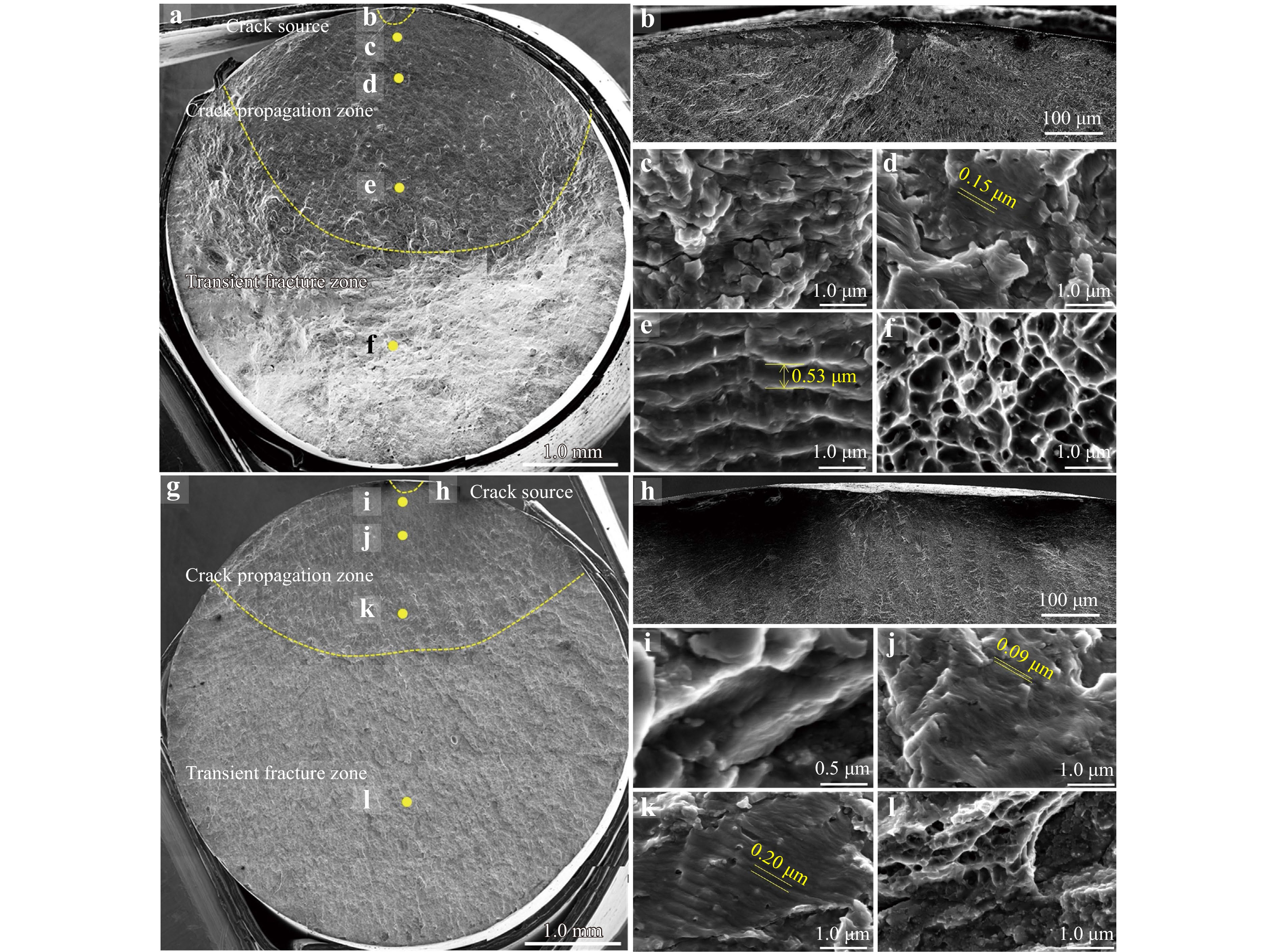

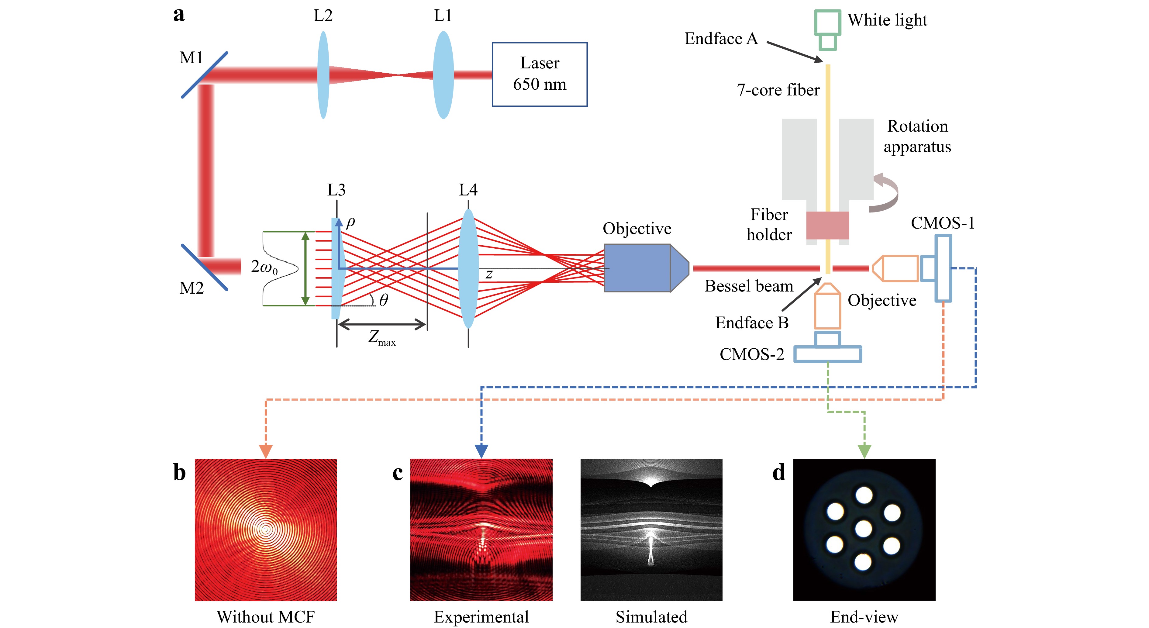
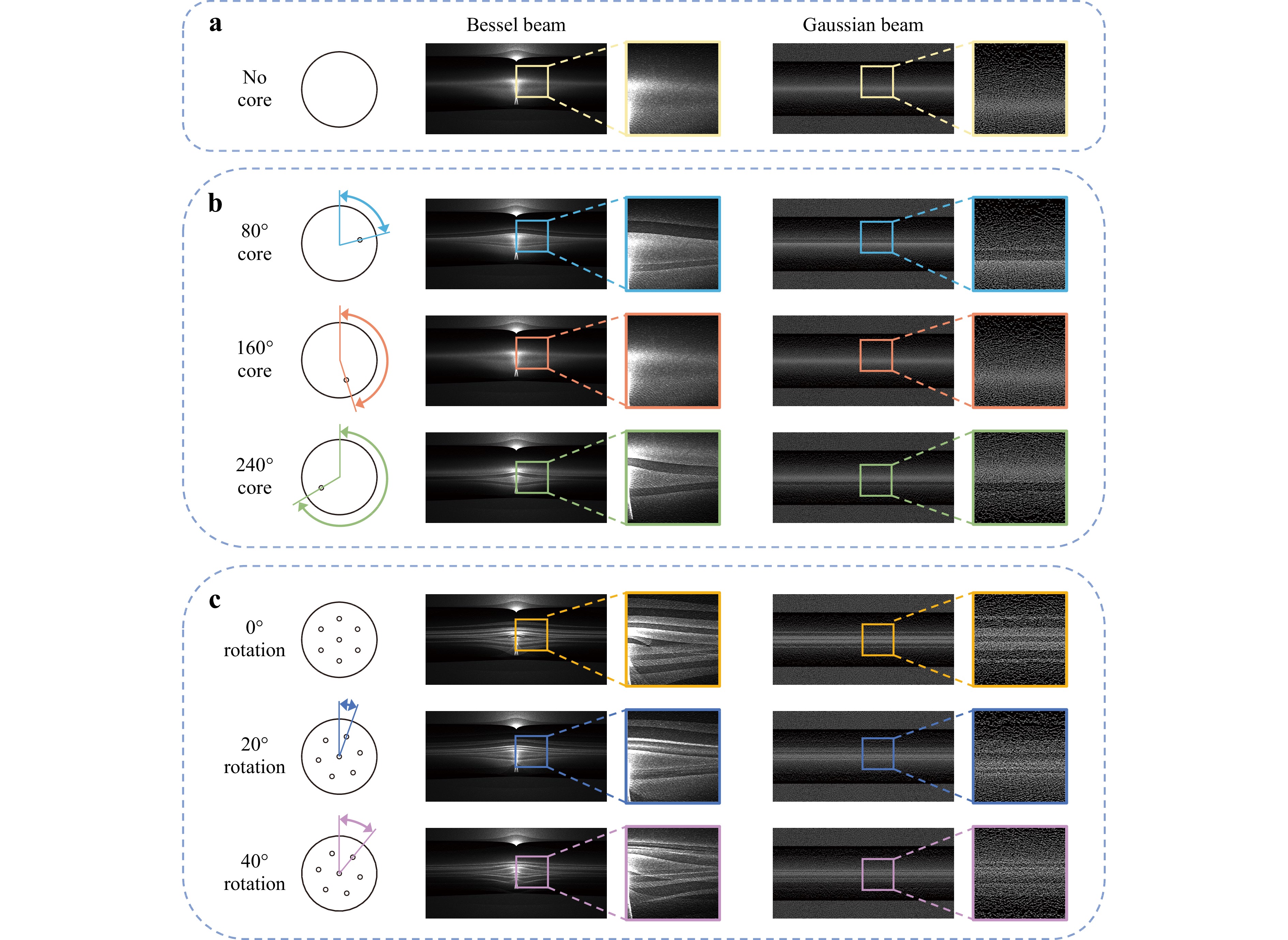
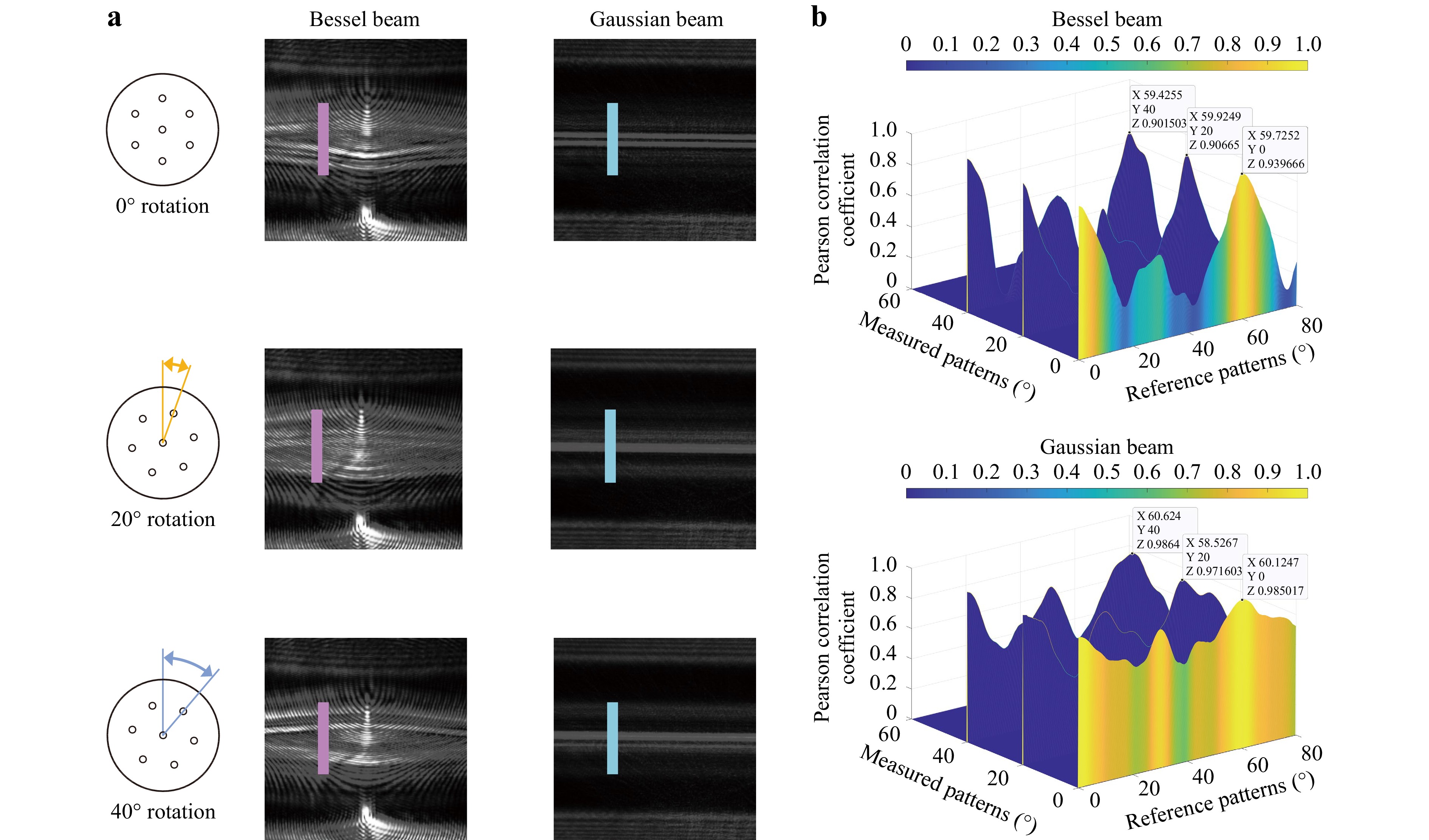
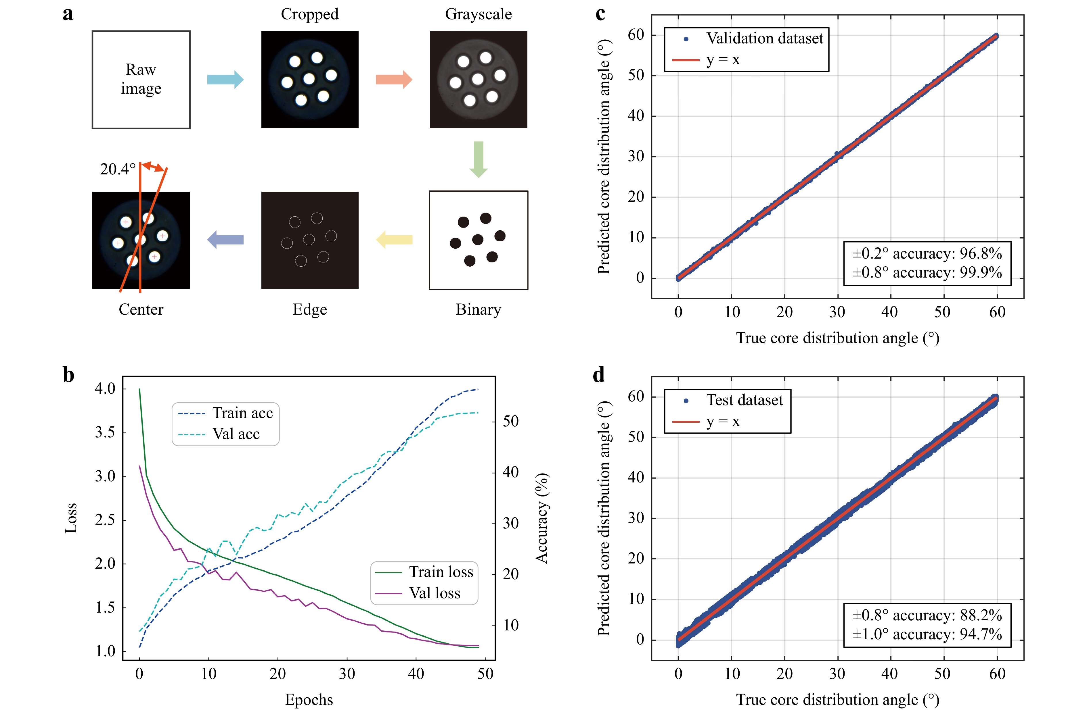
Accurate knowledge of the internal core distribution of multicore fibres (MCFs) is essential, given their widespread application, including in fibre splicing, bundle fan-in/fan-out, mode coupling, writing gratings, and fibre drawing. However, the extensive use of MCFs is restricted by the limited methods available to precisely measure the fibre core distribution, as the measurement accuracy determines the performance of the product. In this study, a side-view and nondestructive scheme based on Bessel beam illumination was proposed for measuring the internal core distribution of a seven-core fibre. Bessel beams offer a large focal length in a scattering medium, and exhibit a unique pattern when propagating in an off-axis medium with a spatially varying refractive index. The results revealed that a long focal length and unique pattern influence the image contrast in the case of Bessel beams, which differs from a typical Gaussian beam. Further, high-precision measurement of a seven-core fibre core distribution based on a Bessel beam was demonstrated using a digital correlation method. A deep learning approach was used to improve the measurement precision to 0.2° with an accuracy of 96.8%. The proposed side-view Bessel-beam-based method has the potential to handle more complex MCFs and photonic crystal fibres.
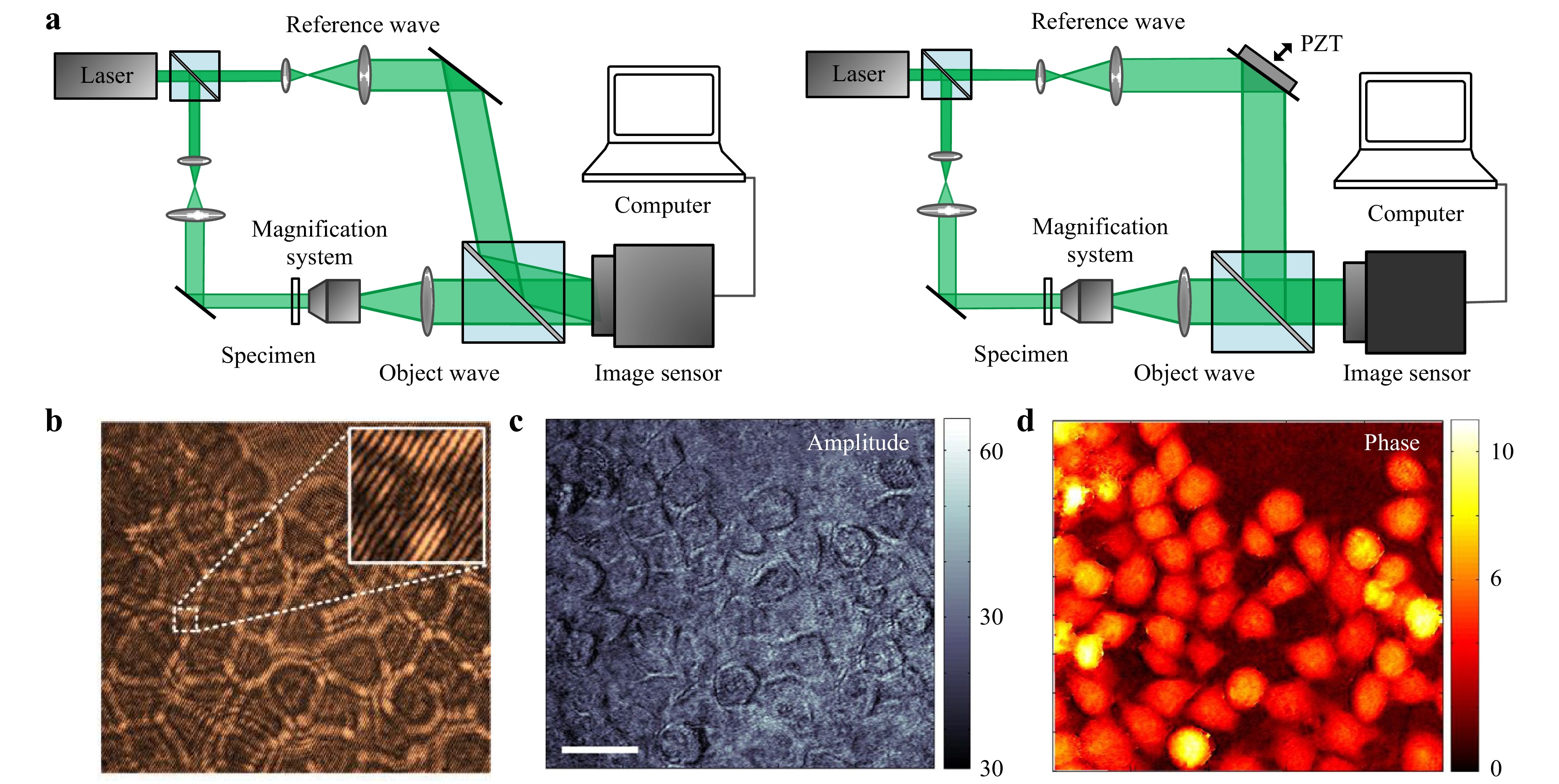
Light microscopes are the most widely used devices in life and material sciences that allow the study of the interaction of light with matter at a resolution better than that of the naked eye. Conventional microscopes translate the spatial differences in the intensity of the reflected or transmitted light from an object to pixel brightness differences in the digital image. However, a phase microscope converts the spatial differences in the phase of the light from or through an object to differences in pixel brightness. Interference microscopy, a phase-based approach, has found application in various disciplines. While interferometry has brought nanometric axial resolution, the lateral resolution in quantitative phase microscopy (QPM) has still remained limited by diffraction, similar to other traditional microscopy systems. Enhancing the resolution has been the subject of intense investigation since the invention of the microscope in the 17th century. During the past decade, microsphere-assisted microscopy (MAM) has emerged as a simple and effective approach to enhance the resolution in light microscopy. MAM can be integrated with QPM for 3D label-free imaging with enhanced resolution. Here, we review the integration of microspheres with coherence scanning interference and digital holographic microscopies, discussing the associated open questions, challenges, and opportunities.
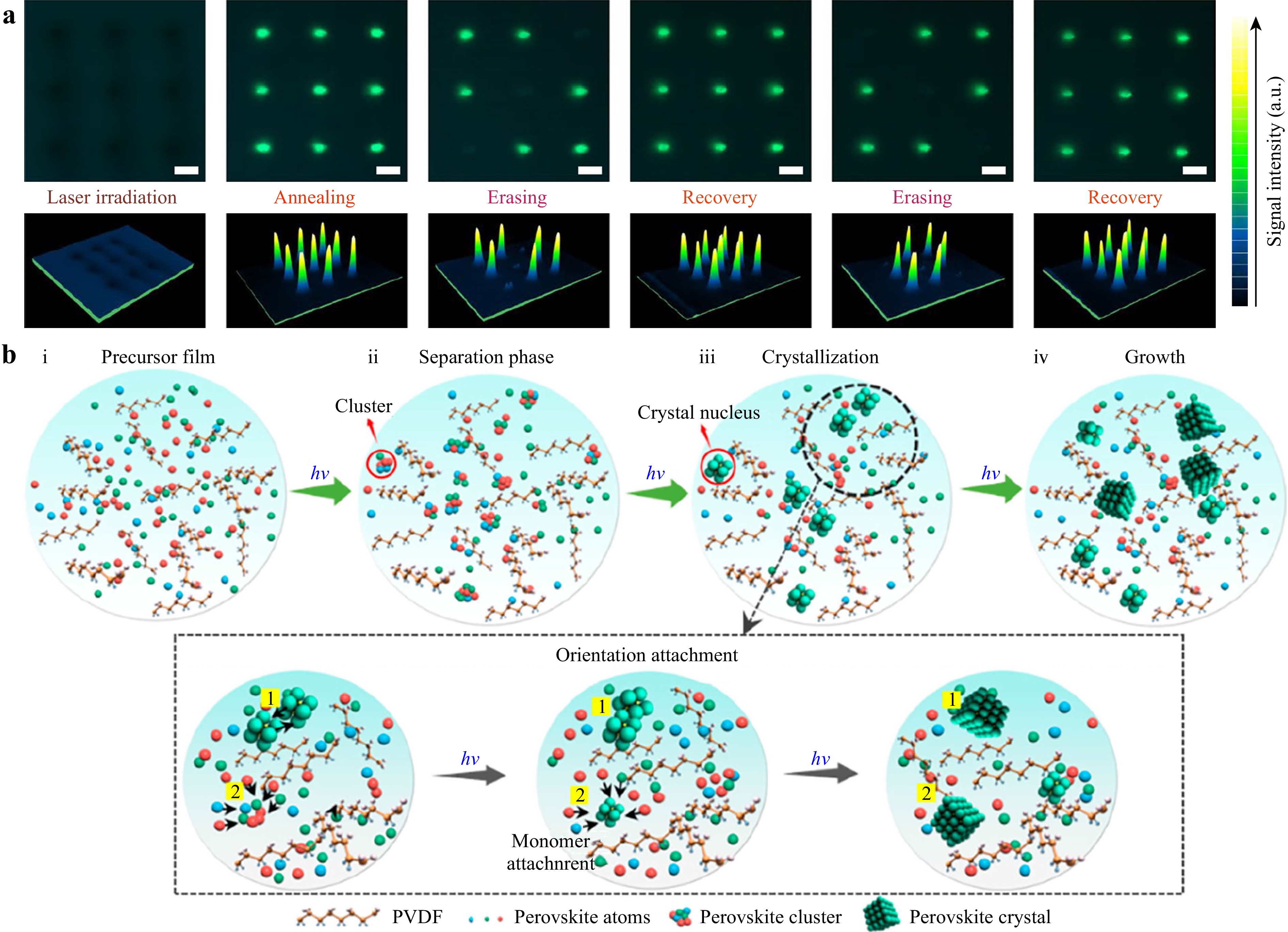
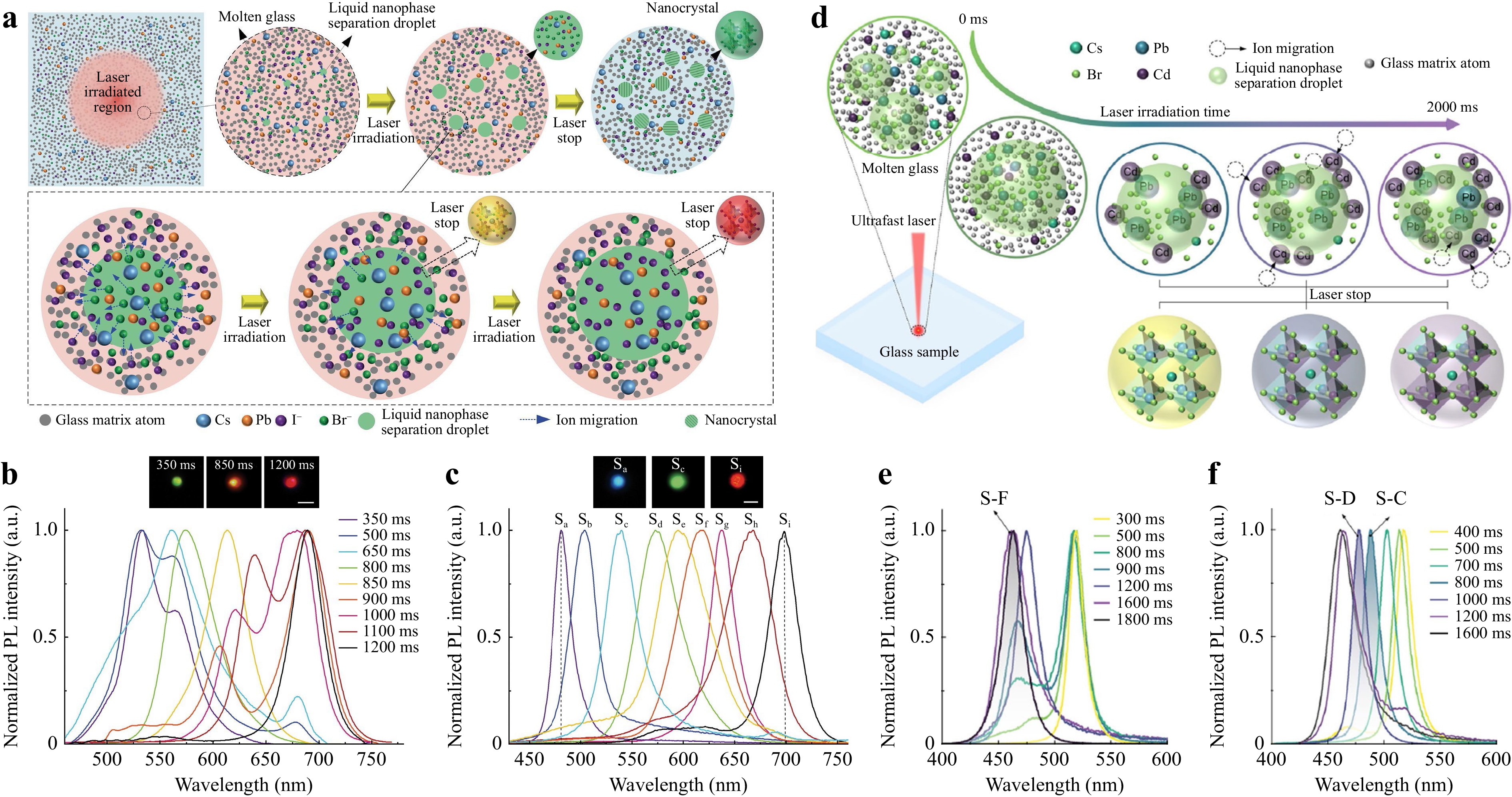
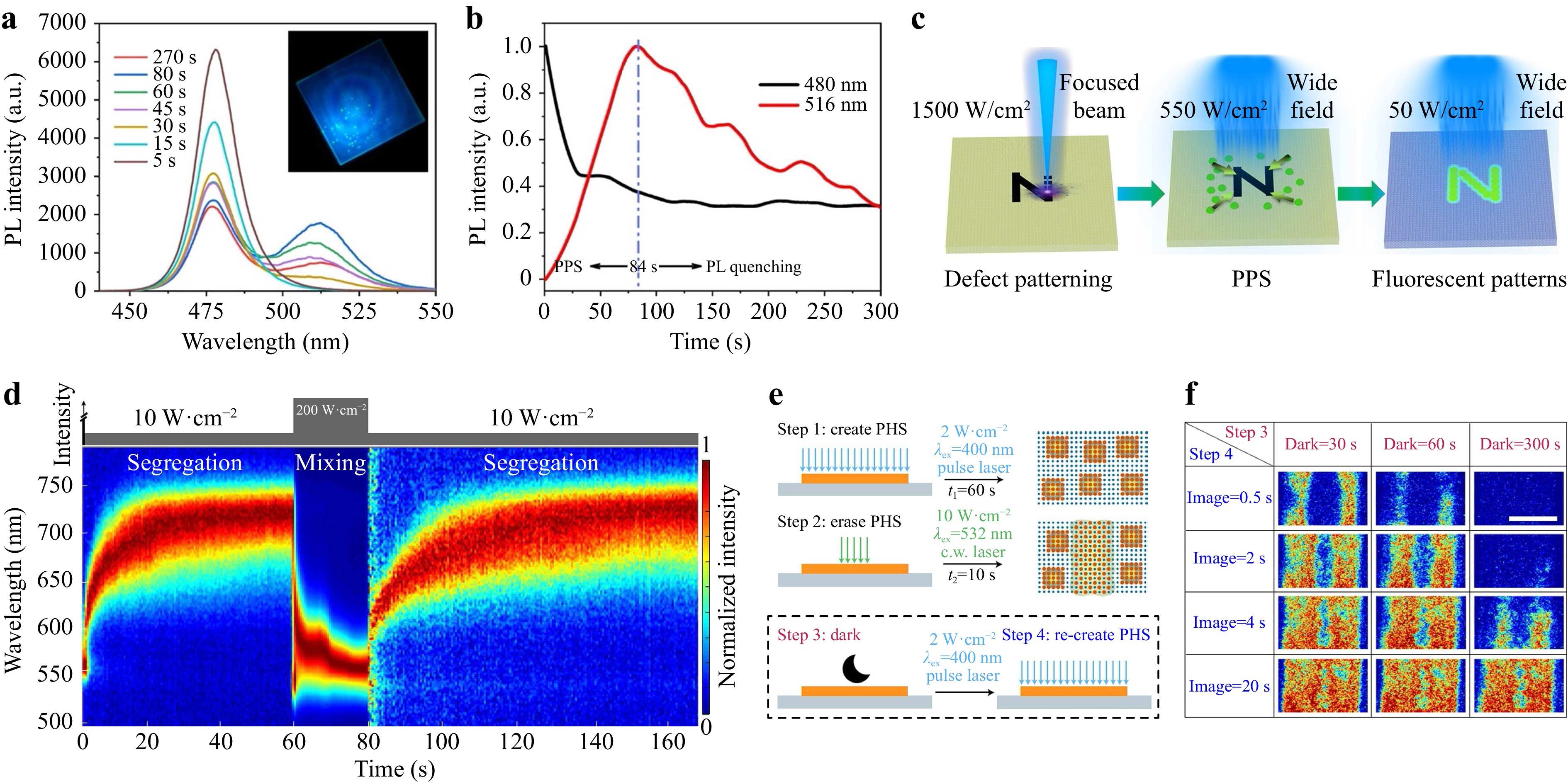
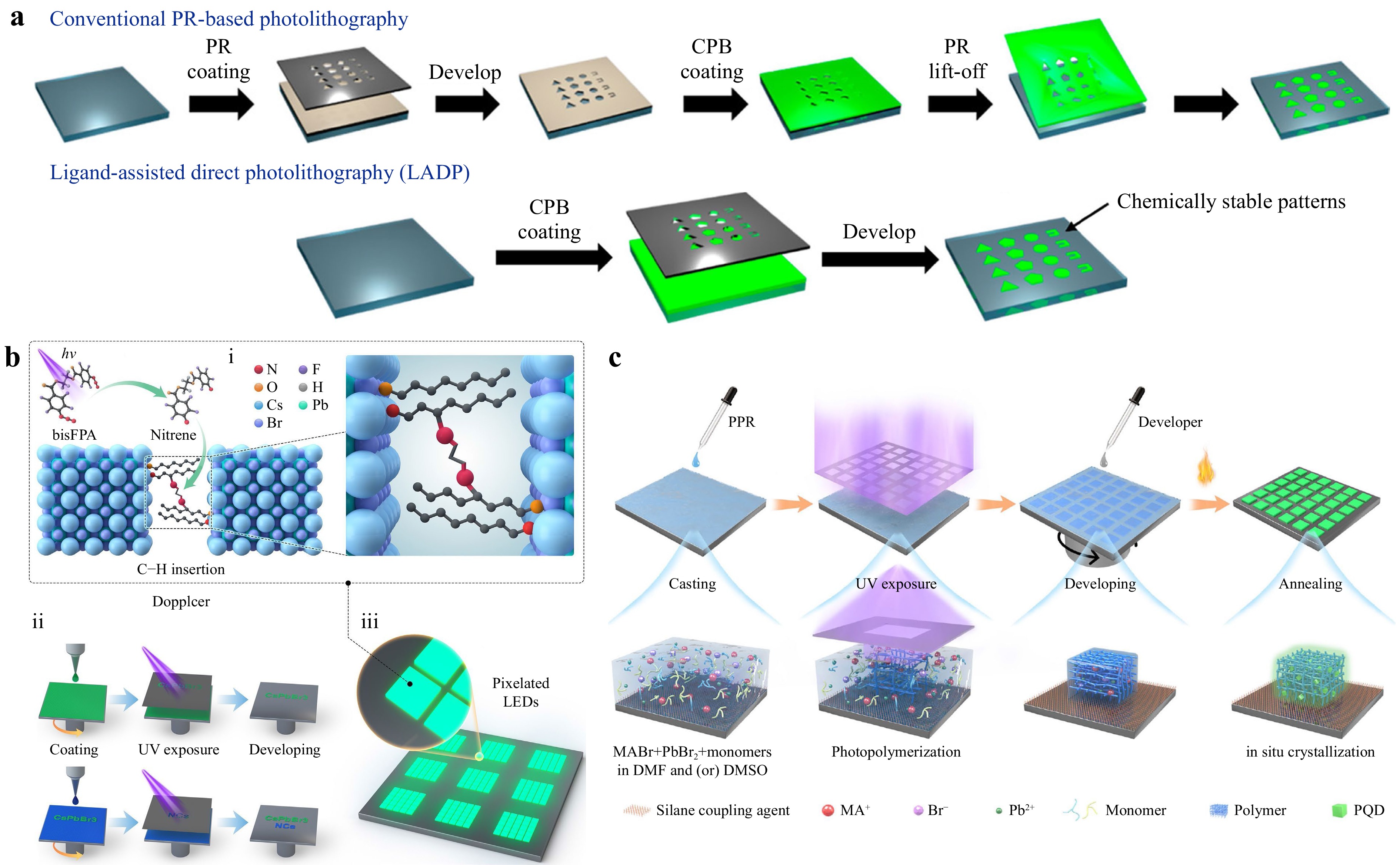
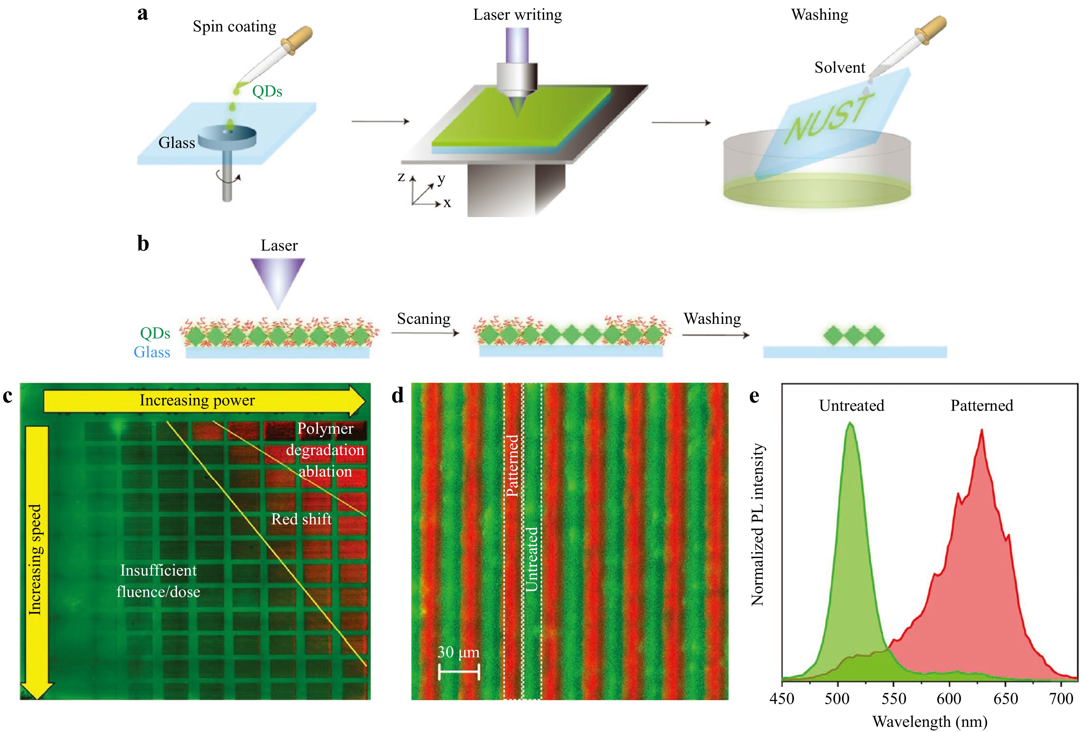
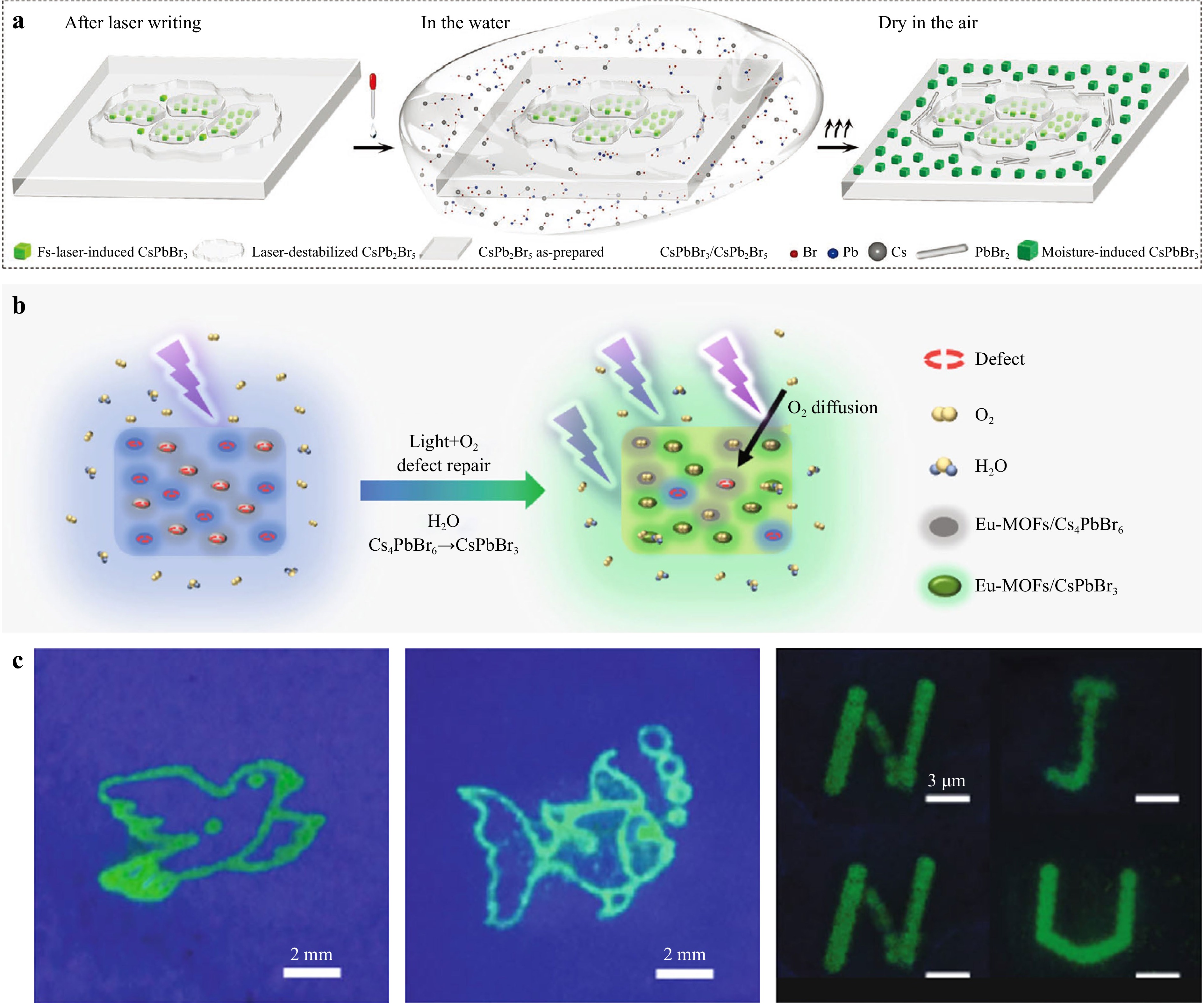
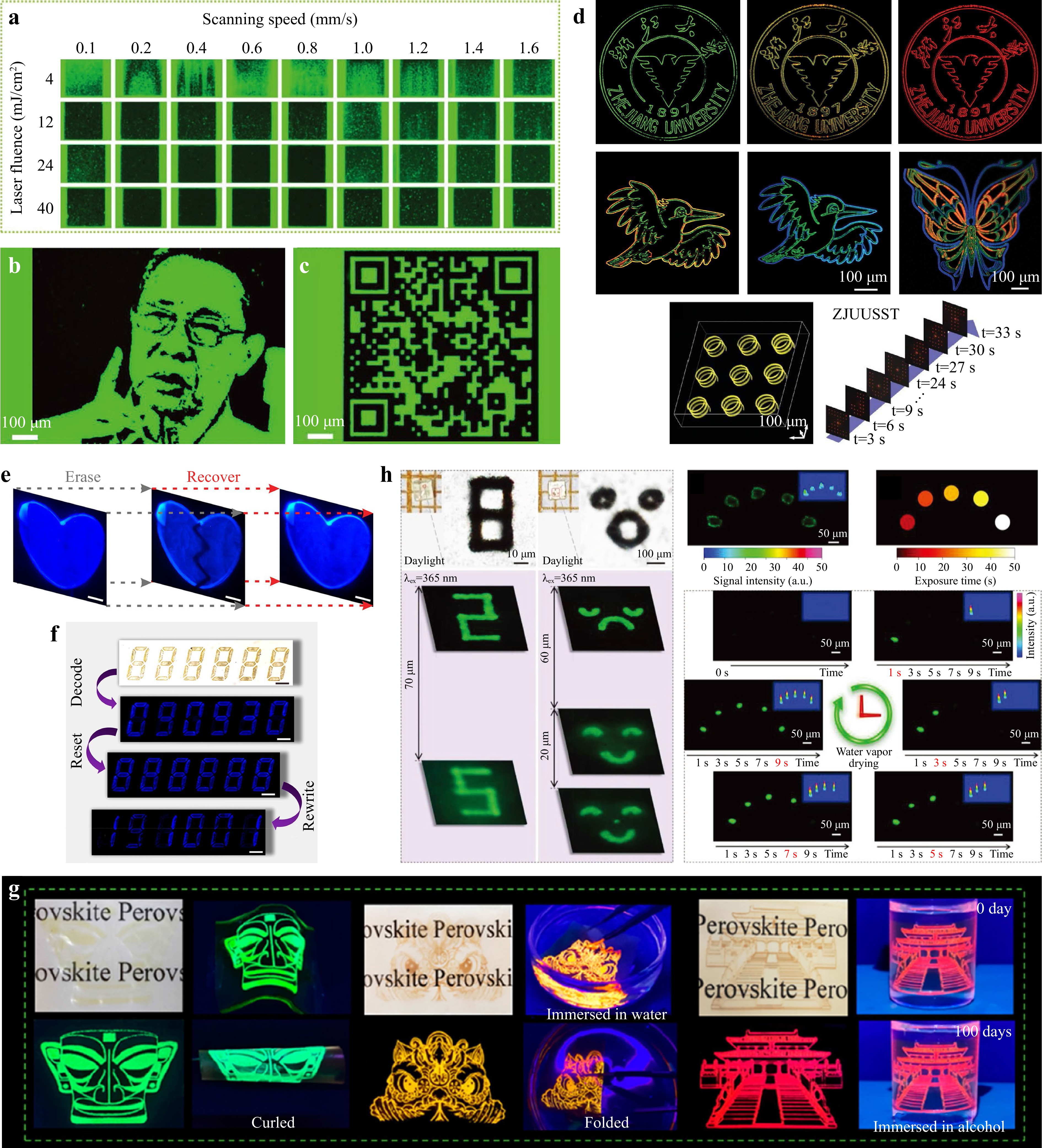
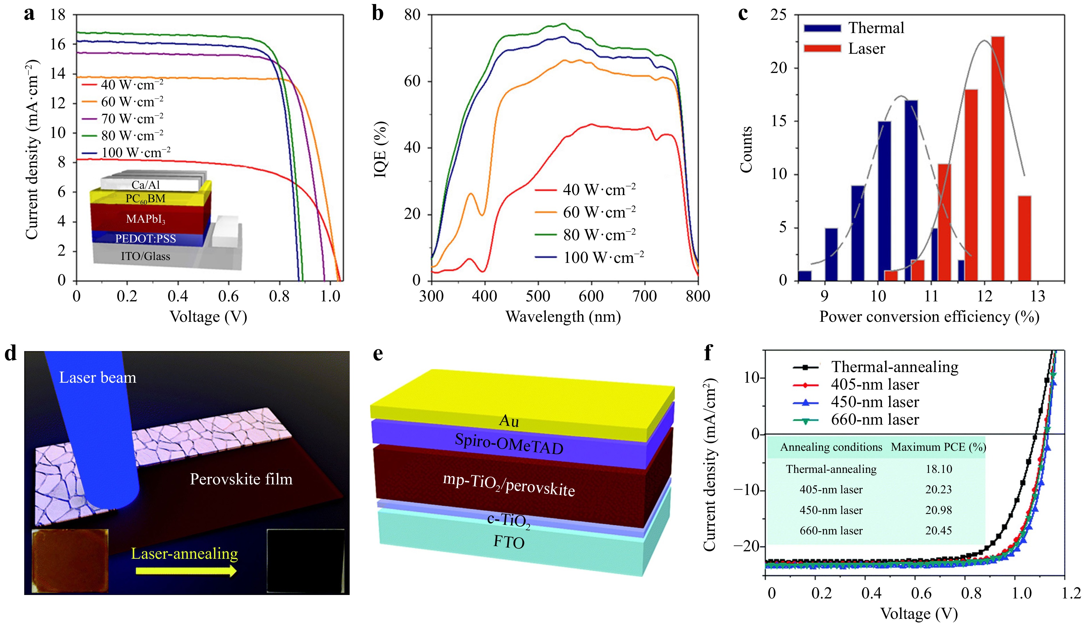
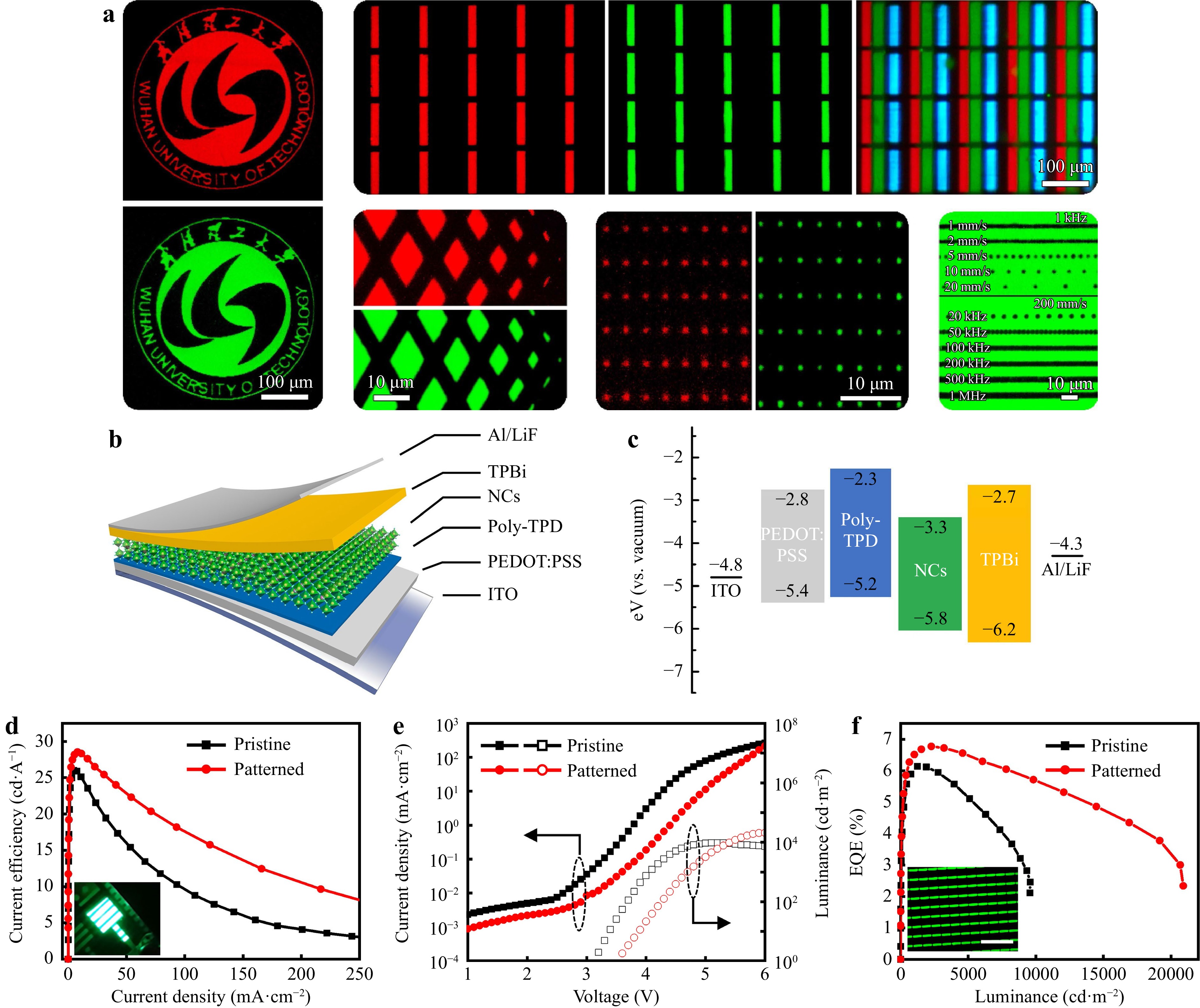
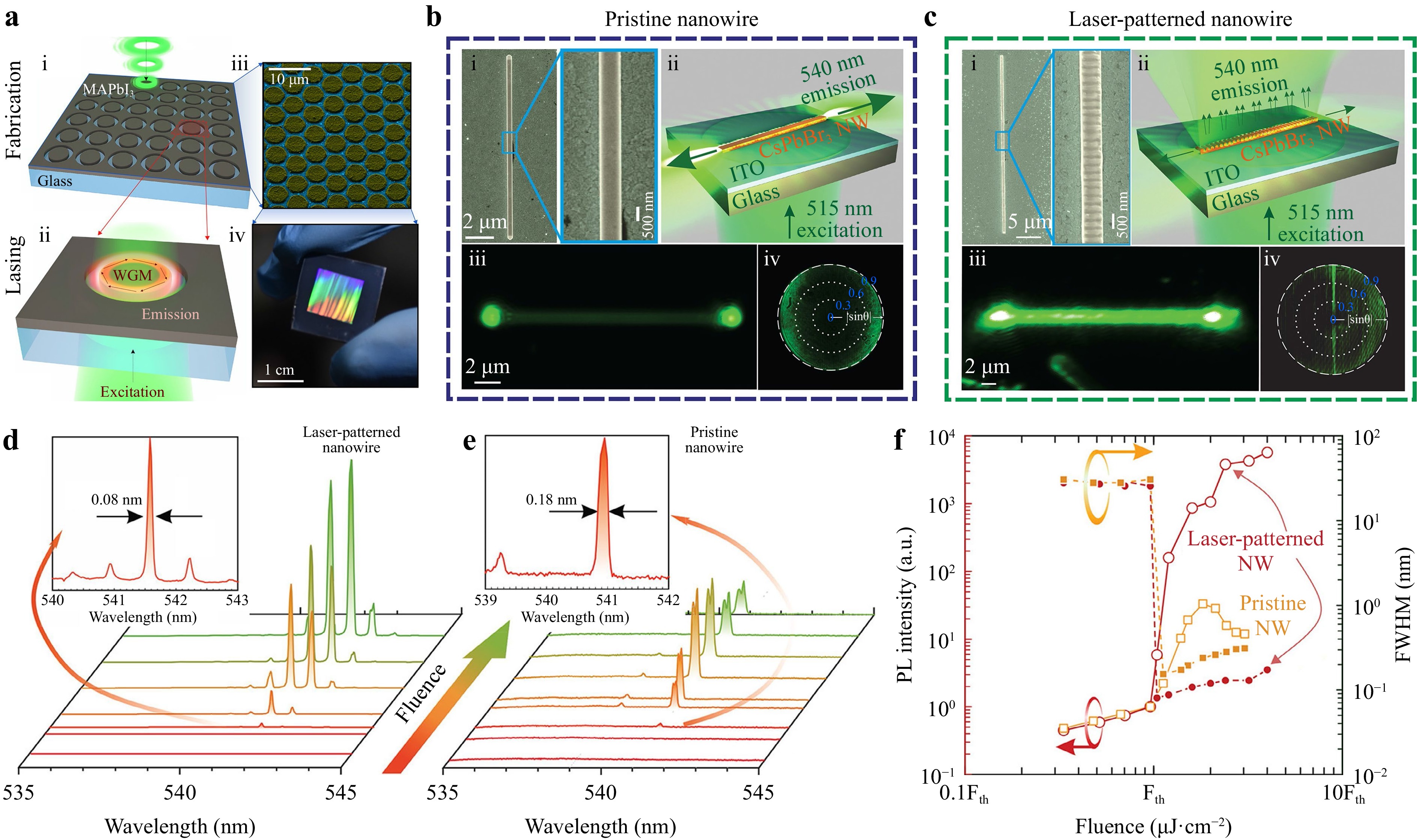
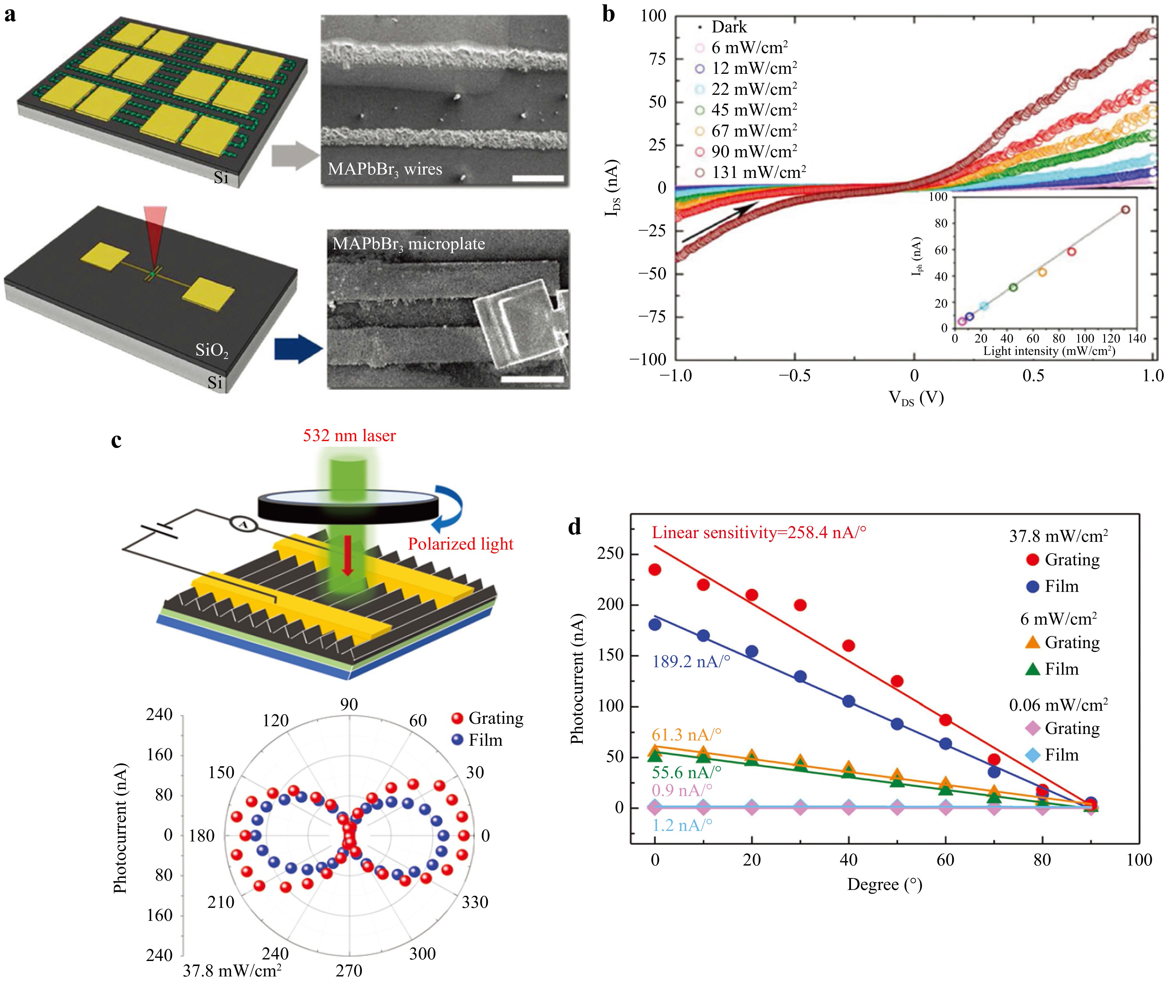
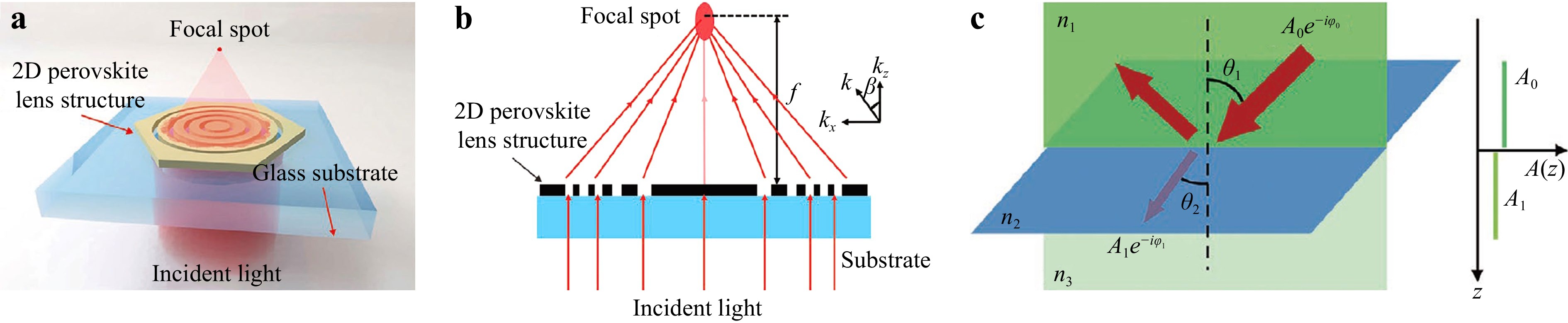
Metal halide perovskites have emerged as game-changing semiconductor materials in optoelectronics. As an efficient micro-/nano-manufacturing technology, direct laser writing (DLW) has been extensively used to fabricate patterns, micro/nanostructures, and pixel arrays on perovskites to promote their optoelectronic applications. Owing to the unique ionic properties and soft lattices of perovskites, DLW can introduce rich light–matter interactions, including laser ablation, crystallisation, ion migration, phase segregation, photoreaction, and other transitions, which enable diverse functionalities in addition to the intrinsic properties of perovskites. Based on their patterned structures, perovskites have numerous applications in displays, optical information encryption, solar cells, light-emitting diodes, lasers, photodetectors, and planar lenses, which are comprehensively discussed in this review. Finally, we discuss the challenges that must be addressed for the future development of this fascinating field.
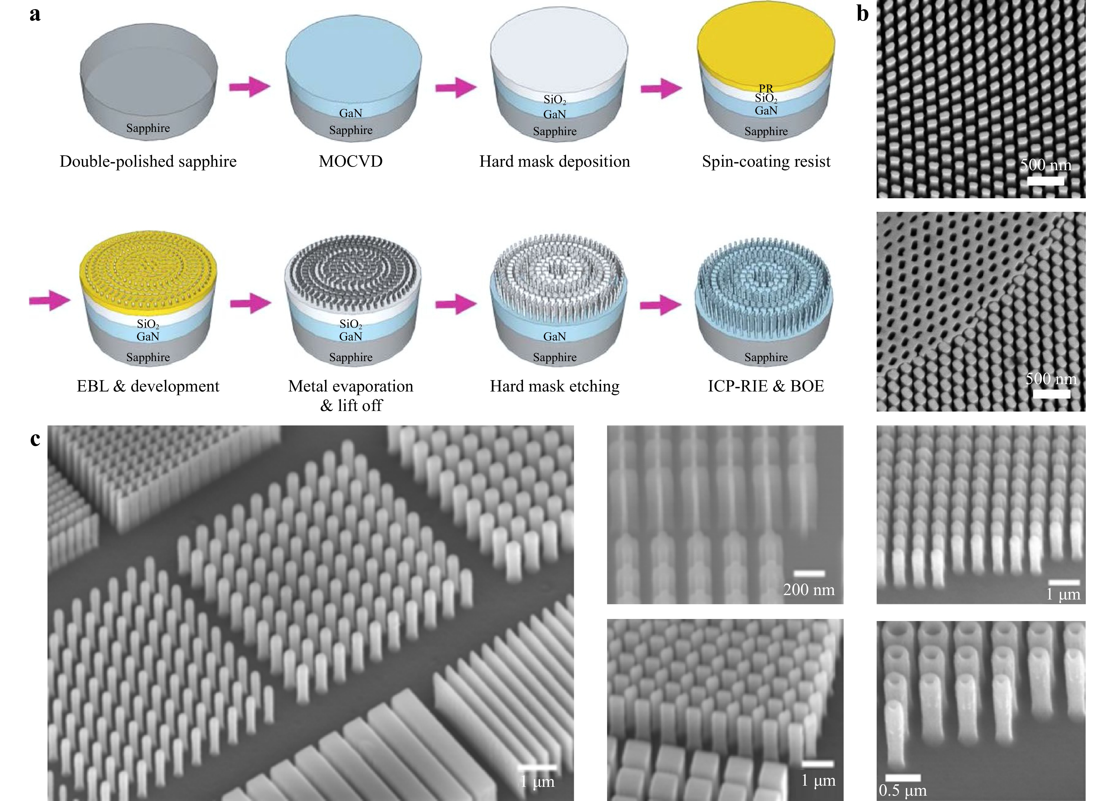
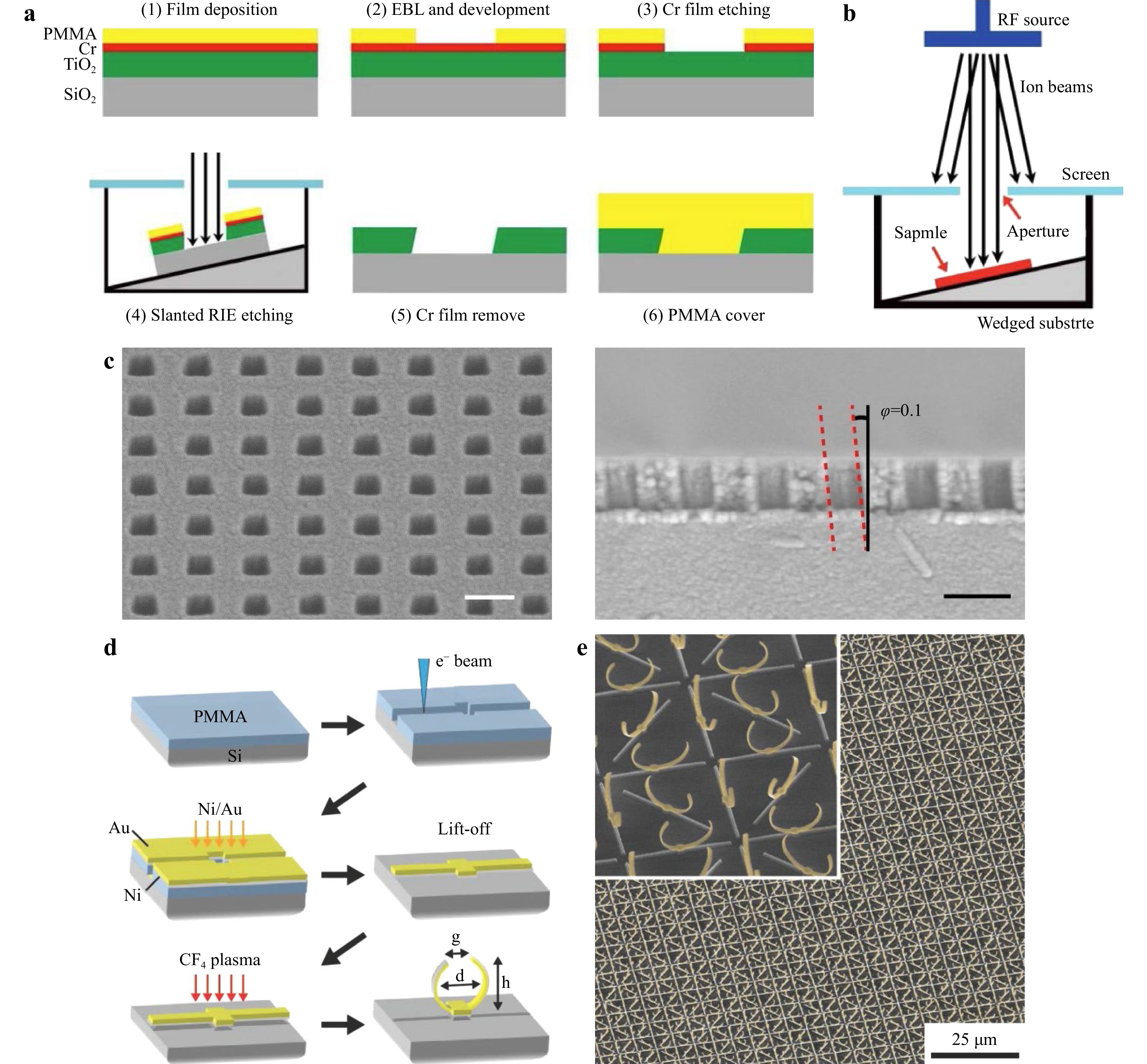
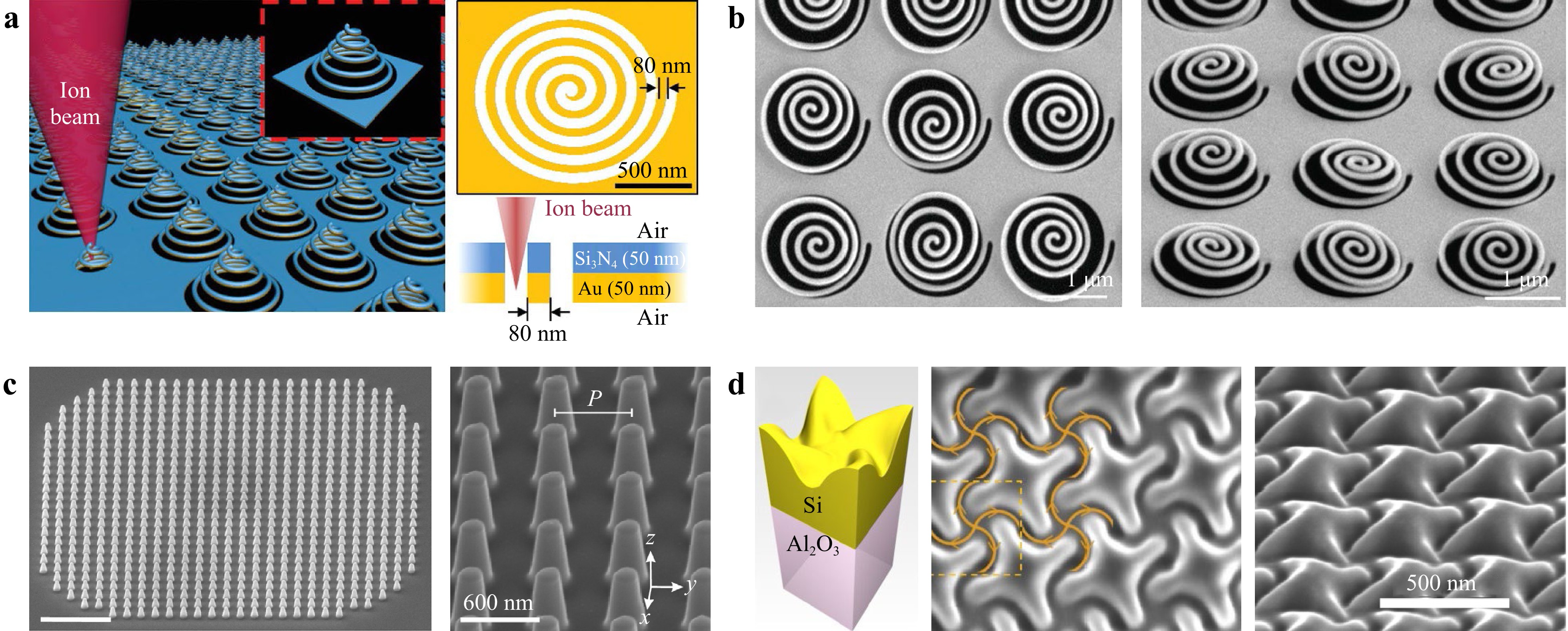
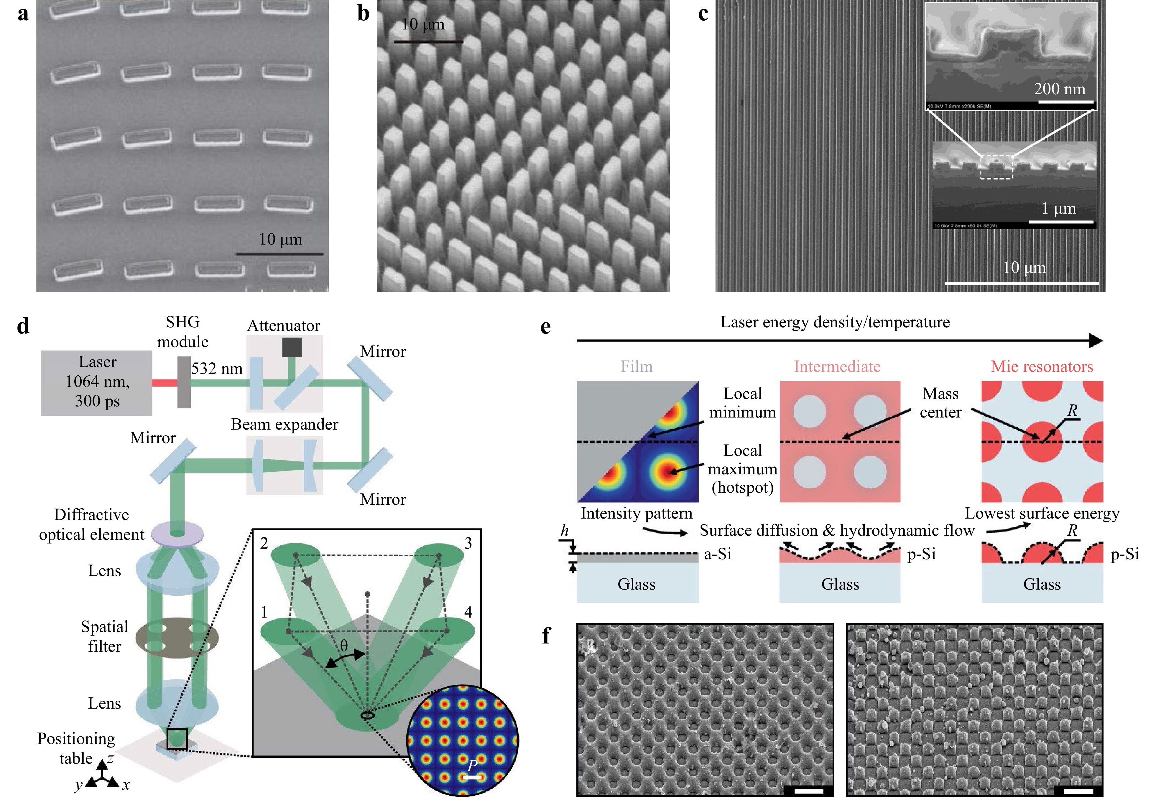
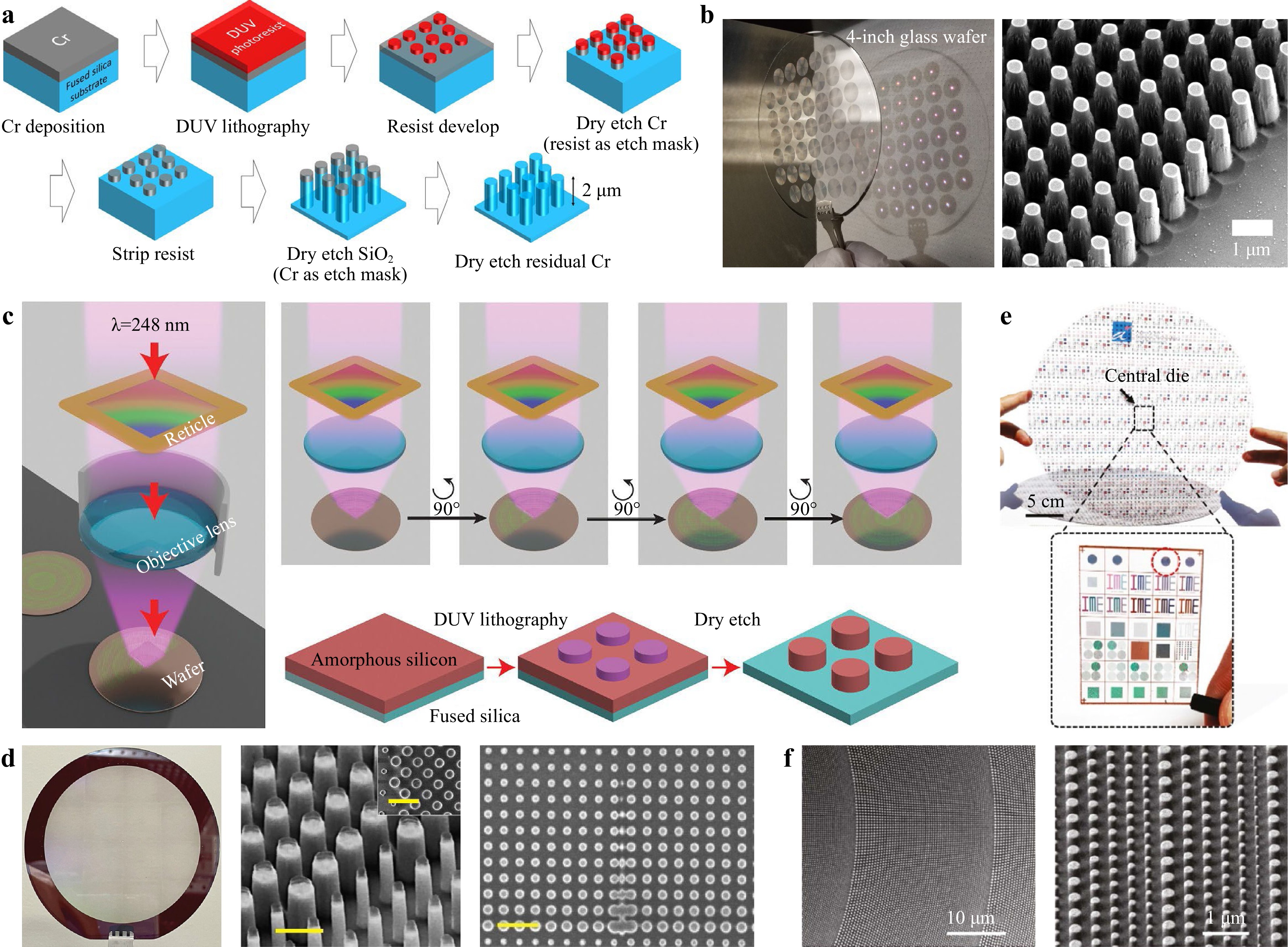
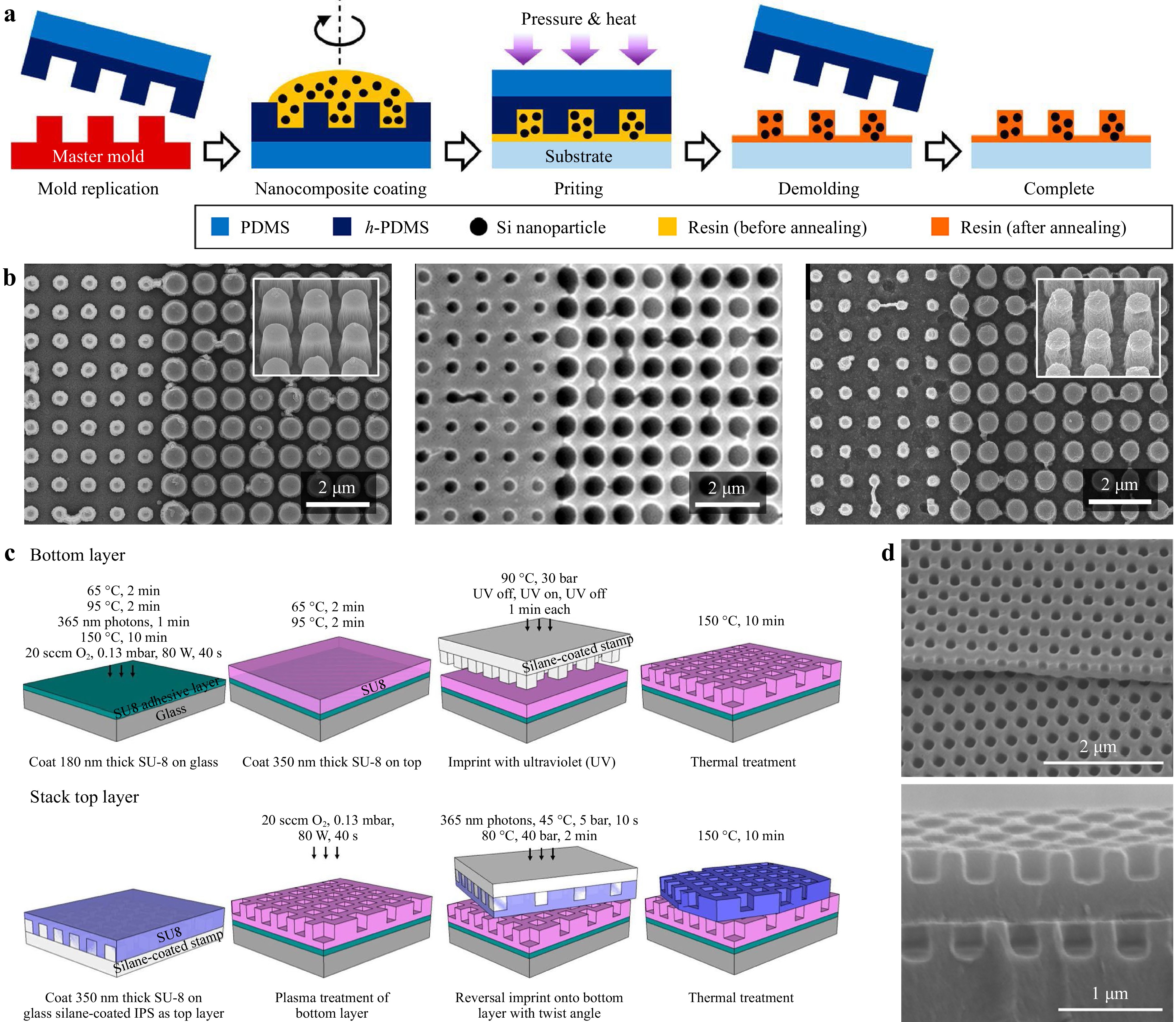
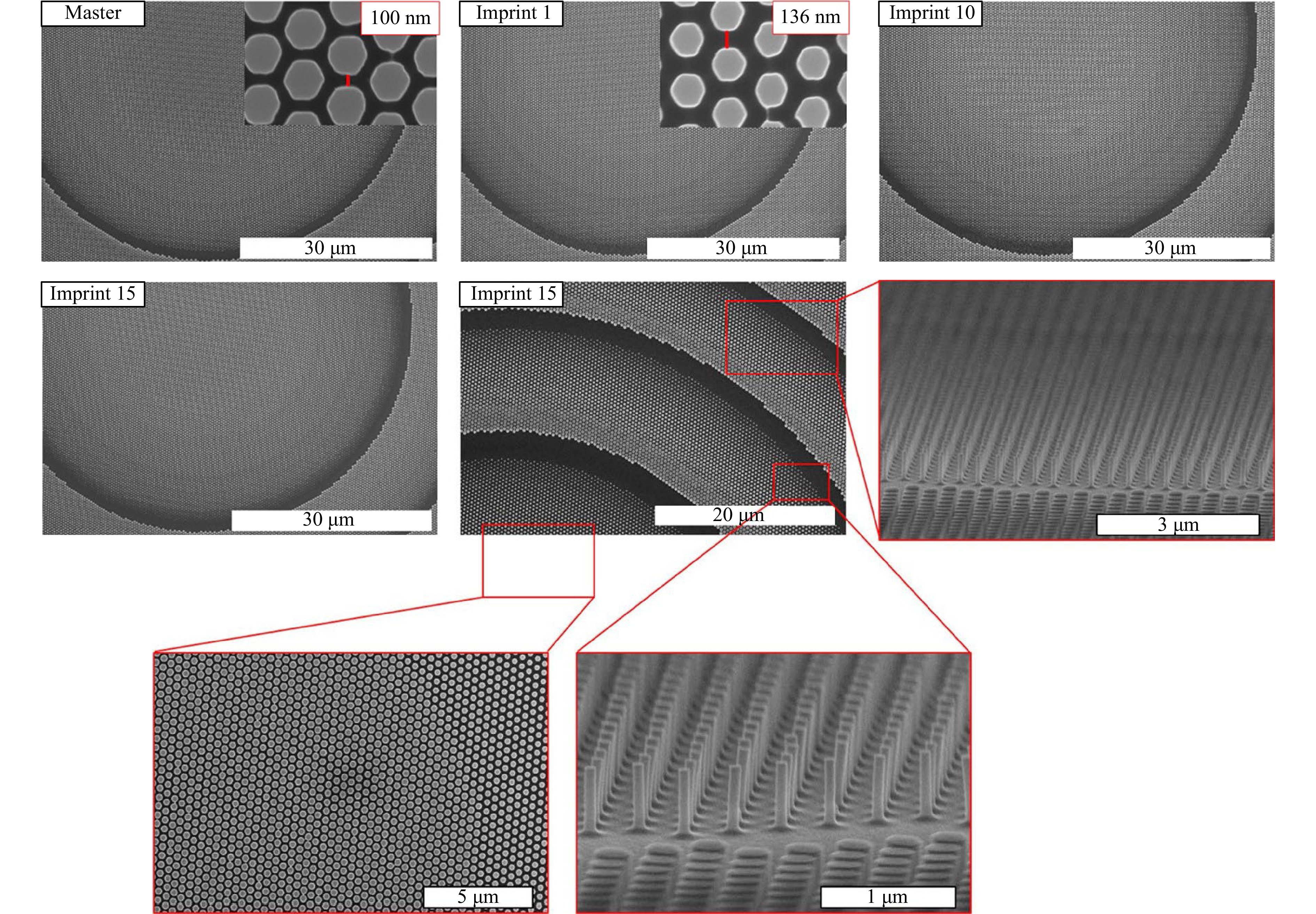
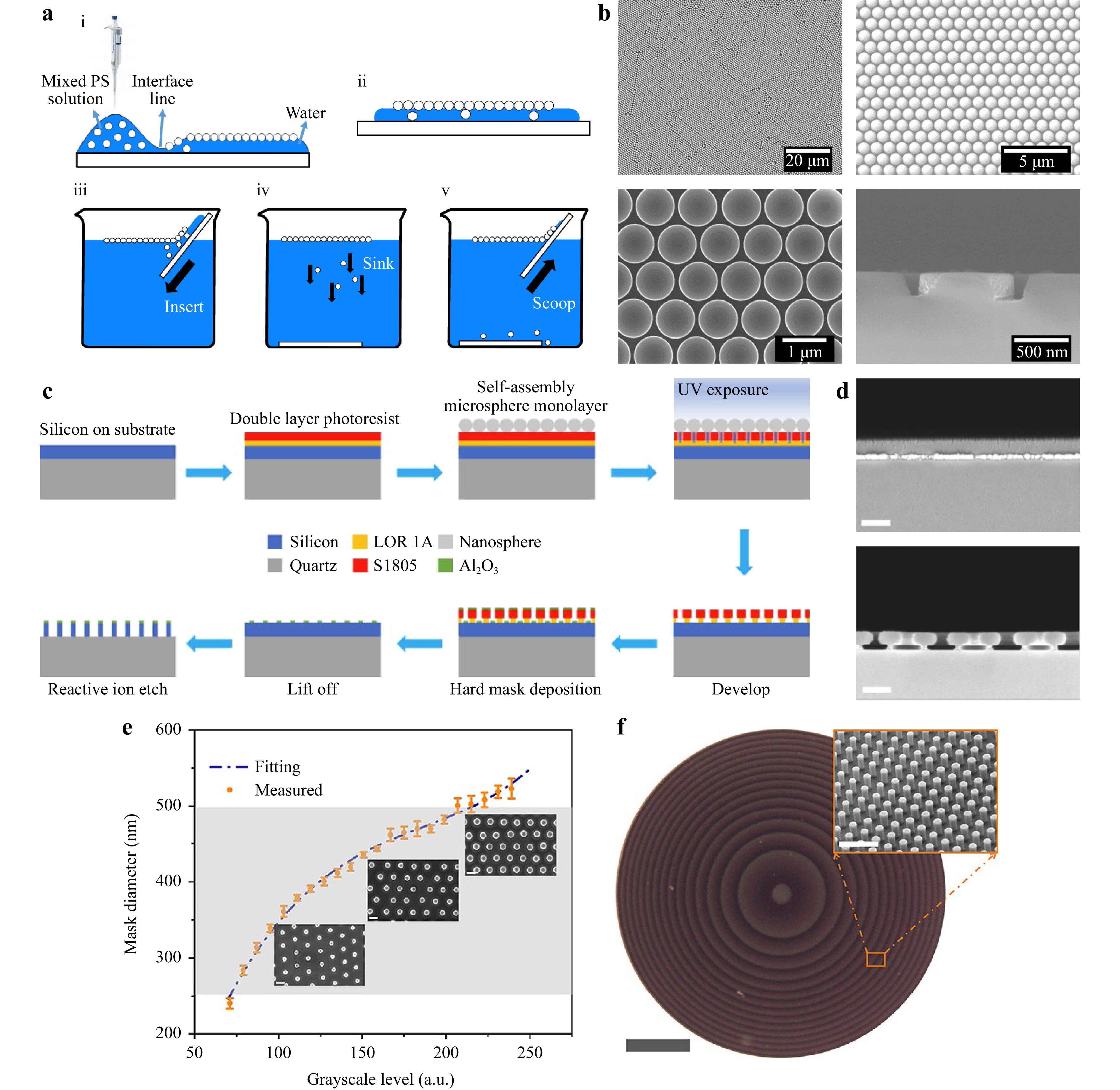
Metasurfaces are one of the most promising devices to break through the limitations of bulky optical components. By offering a new method of light manipulation based on the light-matter interaction in subwavelength nanostructures, metasurfaces enable the efficient manipulation of the amplitude, phase, polarization, and frequency of light and derive a series of possibilities for important applications. However, one key challenge for the realization of applications for meta-devices is how to fabricate large-scale, uniform nanostructures with high resolution. In this review, we review the state-of-the-art nanofabrication techniques compatible with the manufacture of meta-devices. Maskless lithography, masked lithography, and other nanofabrication techniques are highlighted in detail. We also delve into the constraints and limitations of the current fabrication methods while providing some insights on solutions to overcome these challenges for advanced nanophotonic applications.
ISSN 2689-9620 EISSN 2831-4093
Indexed by:
- DOAJ
- Scopus
- Google Scholar
- CNKI

 Email
Email RSS
RSS-
2021, 2(3): 350-369. doi: 10.37188/lam.2021.024
-
2021, 2(3): 313-332. doi: 10.37188/lam.2021.020
-
2023, 4(3): 233-242. doi: 10.37188/lam.2023.023
-
2021, 2(1): 59-83. doi: 10.37188/lam.2021.005
-
2021, 2(4): 446-459. doi: 10.37188/lam.2021.028