
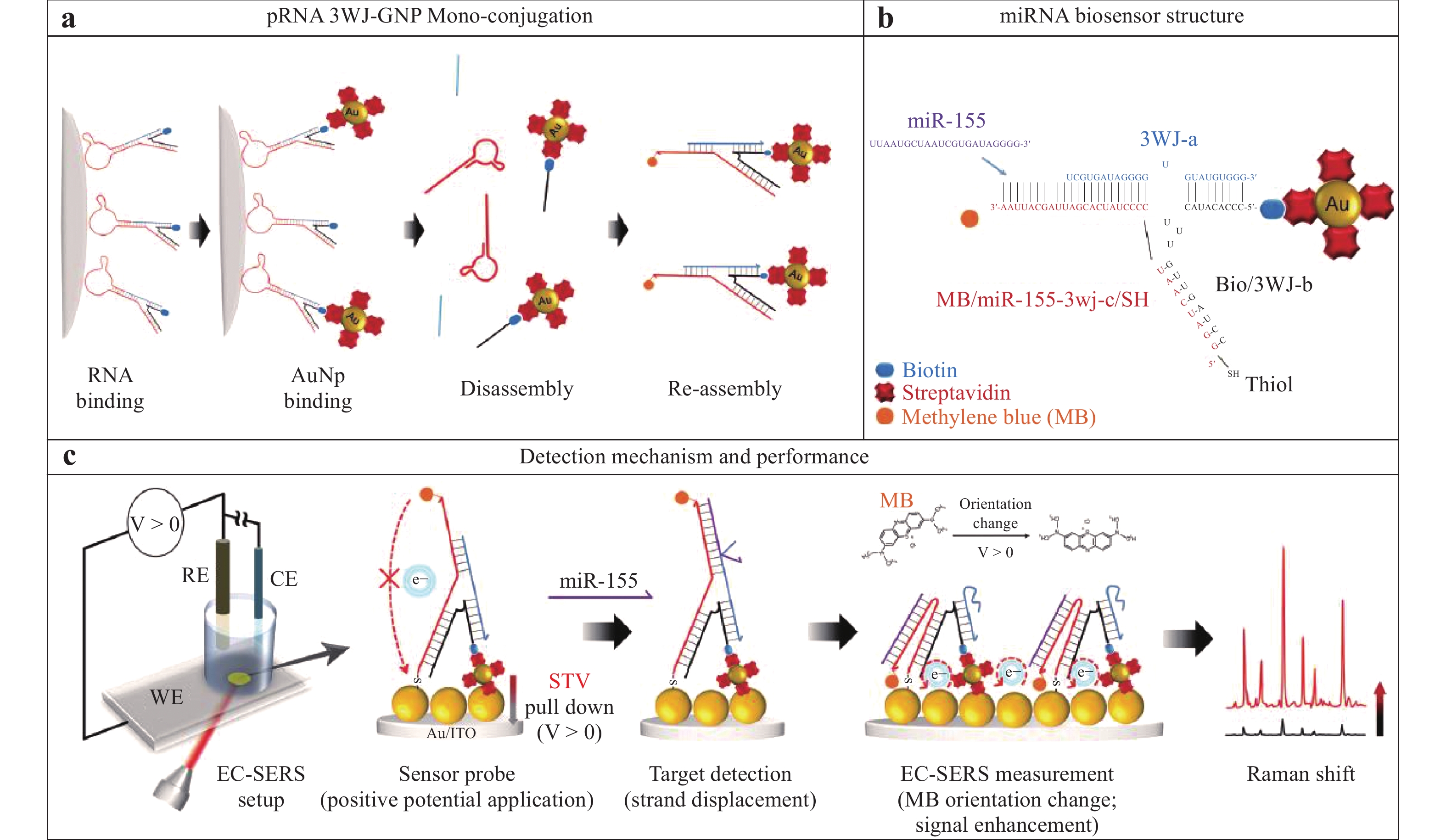
View by Category
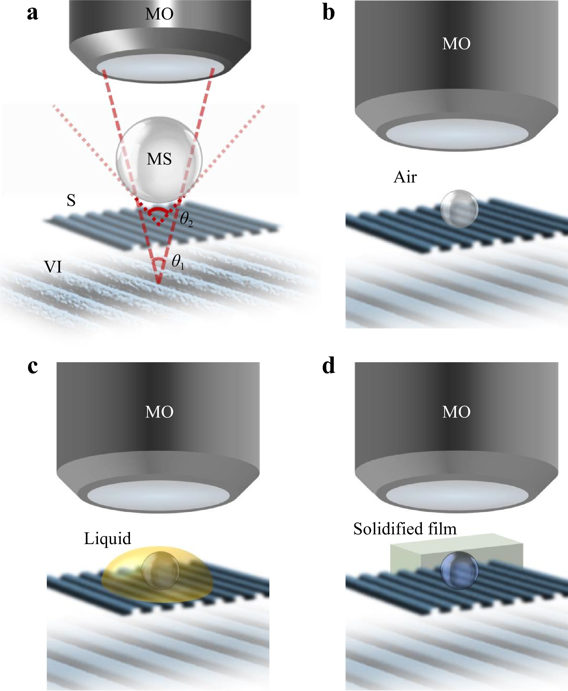
Light microscopes are the most widely used devices in life and material sciences that allow the study of the interaction of light with matter at a resolution better than that of the naked eye. Conventional microscopes translate the spatial differences in the intensity of the reflected or transmitted light from an object to pixel brightness differences in the digital image. However, a phase microscope converts the spatial differences in the phase of the light from or through an object to differences in pixel brightness. Interference microscopy, a phase-based approach, has found application in various disciplines. While interferometry has brought nanometric axial resolution, the lateral resolution in quantitative phase microscopy (QPM) has still remained limited by diffraction, similar to other traditional microscopy systems. Enhancing the resolution has been the subject of intense investigation since the invention of the microscope in the 17th century. During the past decade, microsphere-assisted microscopy (MAM) has emerged as a simple and effective approach to enhance the resolution in light microscopy. MAM can be integrated with QPM for 3D label-free imaging with enhanced resolution. Here, we review the integration of microspheres with coherence scanning interference and digital holographic microscopies, discussing the associated open questions, challenges, and opportunities.


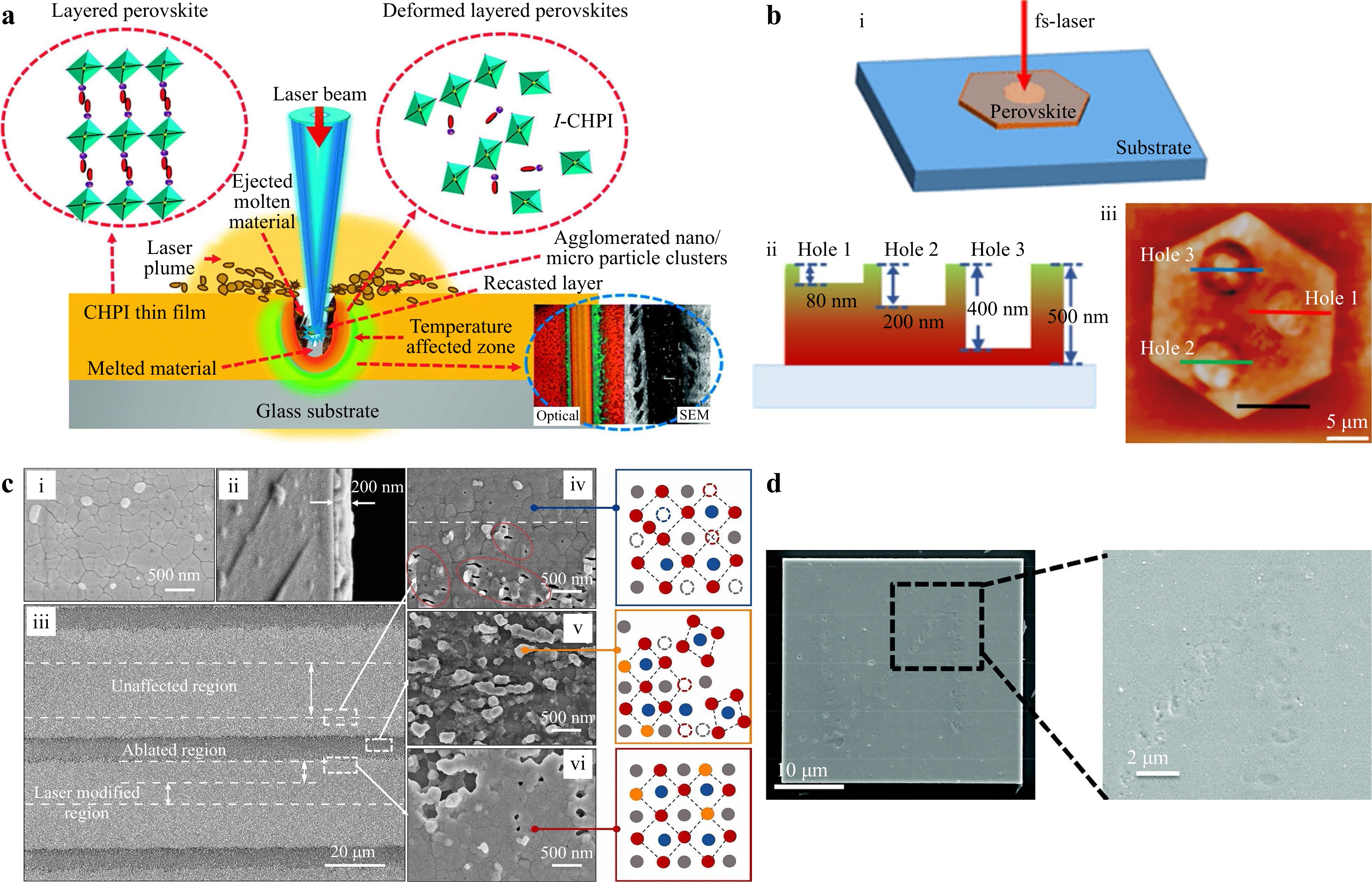
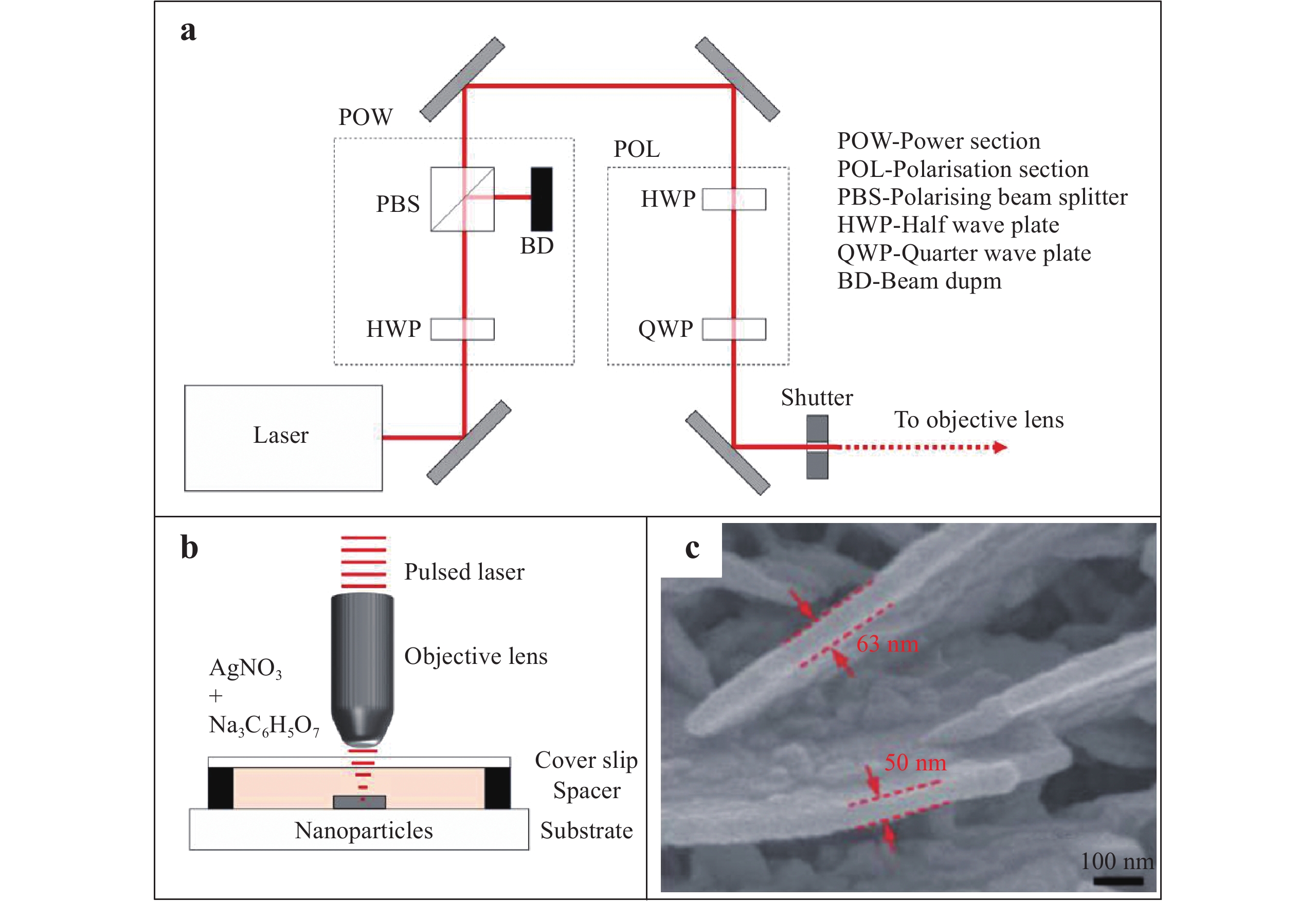
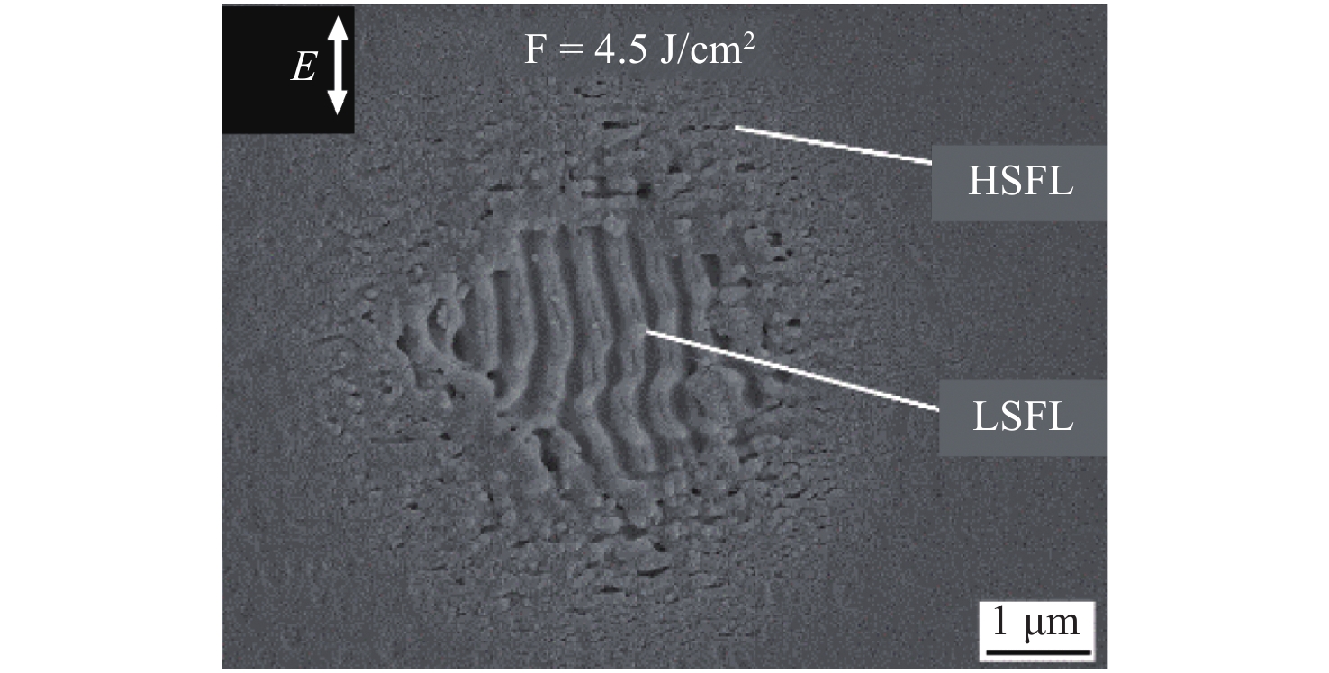
Metal halide perovskites have emerged as game-changing semiconductor materials in optoelectronics. As an efficient micro-/nano-manufacturing technology, direct laser writing (DLW) has been extensively used to fabricate patterns, micro/nanostructures, and pixel arrays on perovskites to promote their optoelectronic applications. Owing to the unique ionic properties and soft lattices of perovskites, DLW can introduce rich light–matter interactions, including laser ablation, crystallisation, ion migration, phase segregation, photoreaction, and other transitions, which enable diverse functionalities in addition to the intrinsic properties of perovskites. Based on their patterned structures, perovskites have numerous applications in displays, optical information encryption, solar cells, light-emitting diodes, lasers, photodetectors, and planar lenses, which are comprehensively discussed in this review. Finally, we discuss the challenges that must be addressed for the future development of this fascinating field.


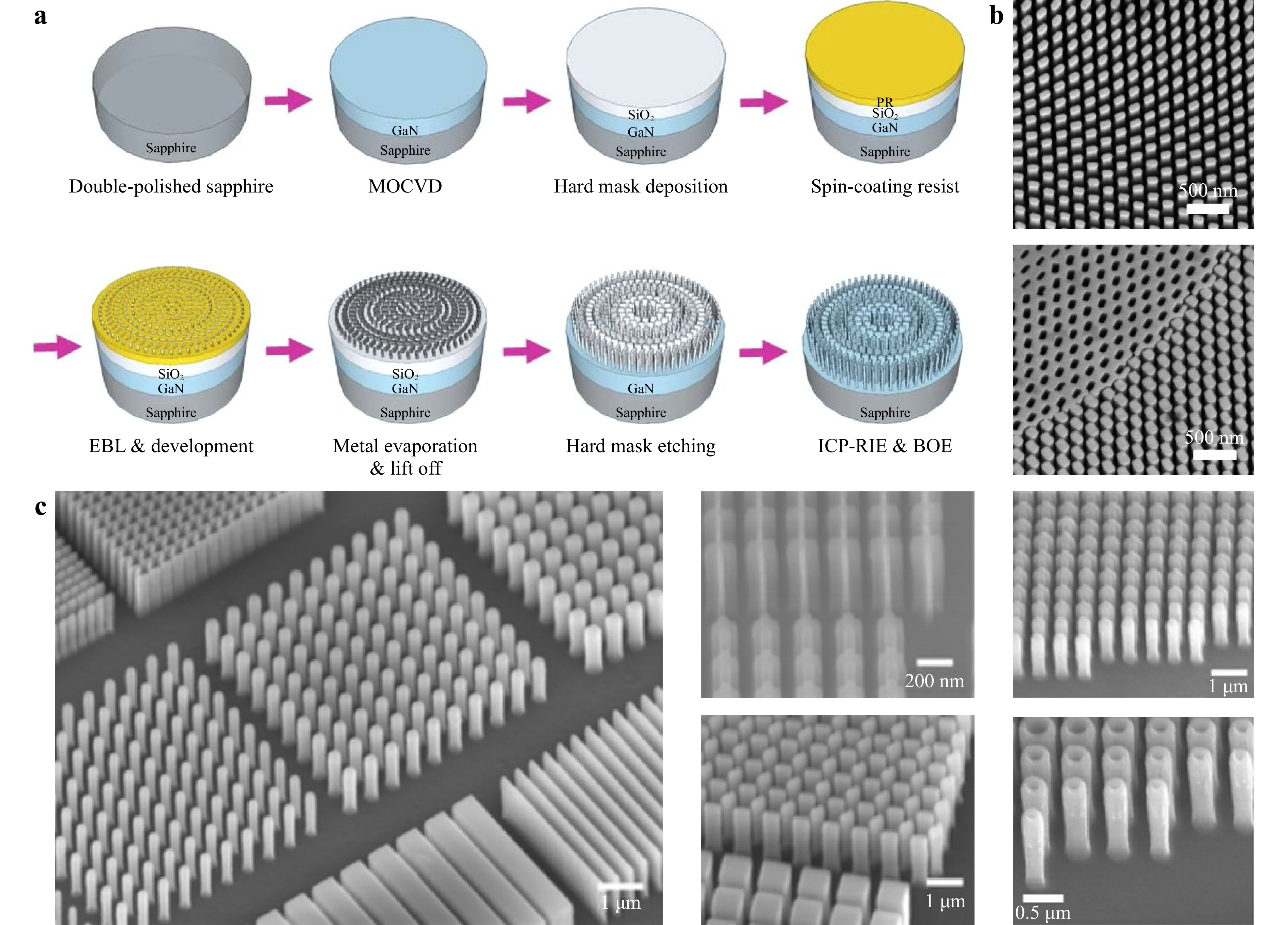
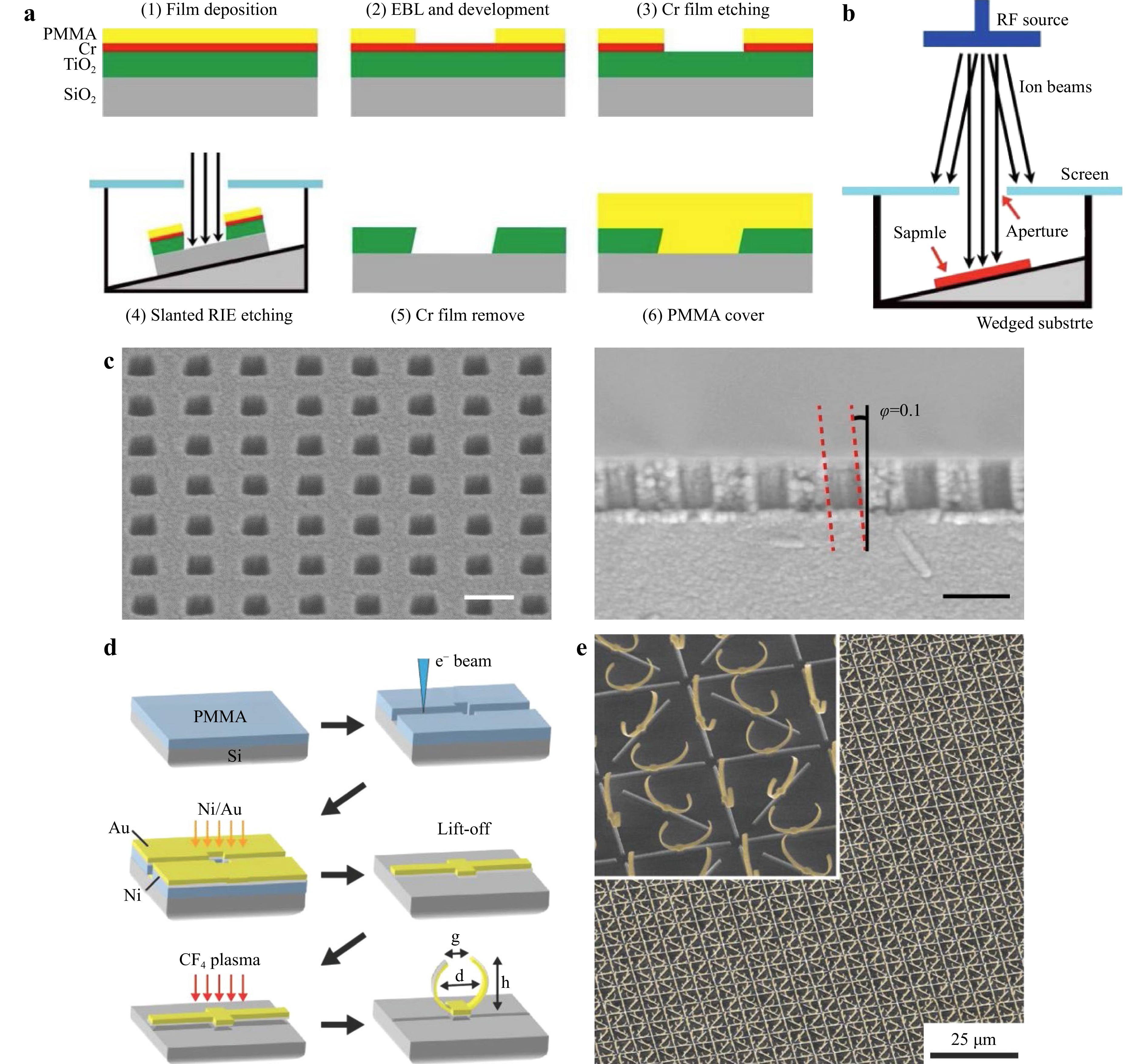
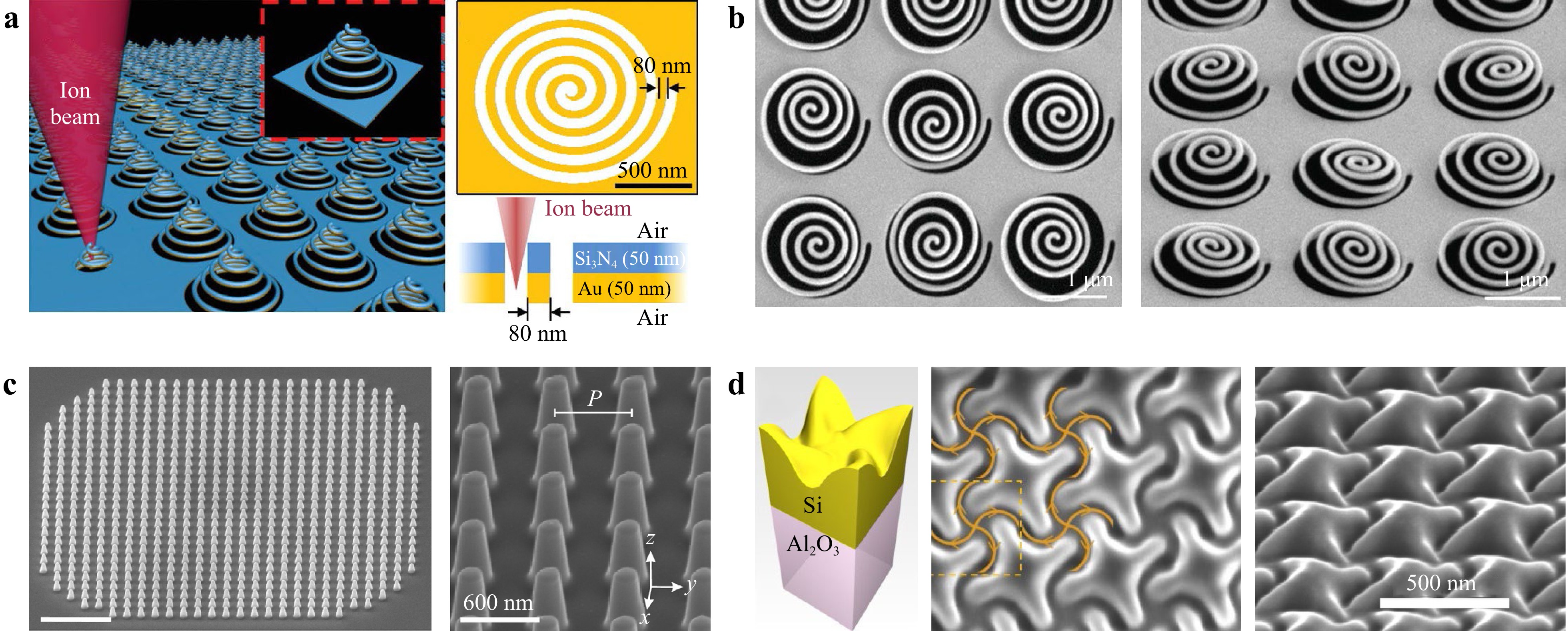
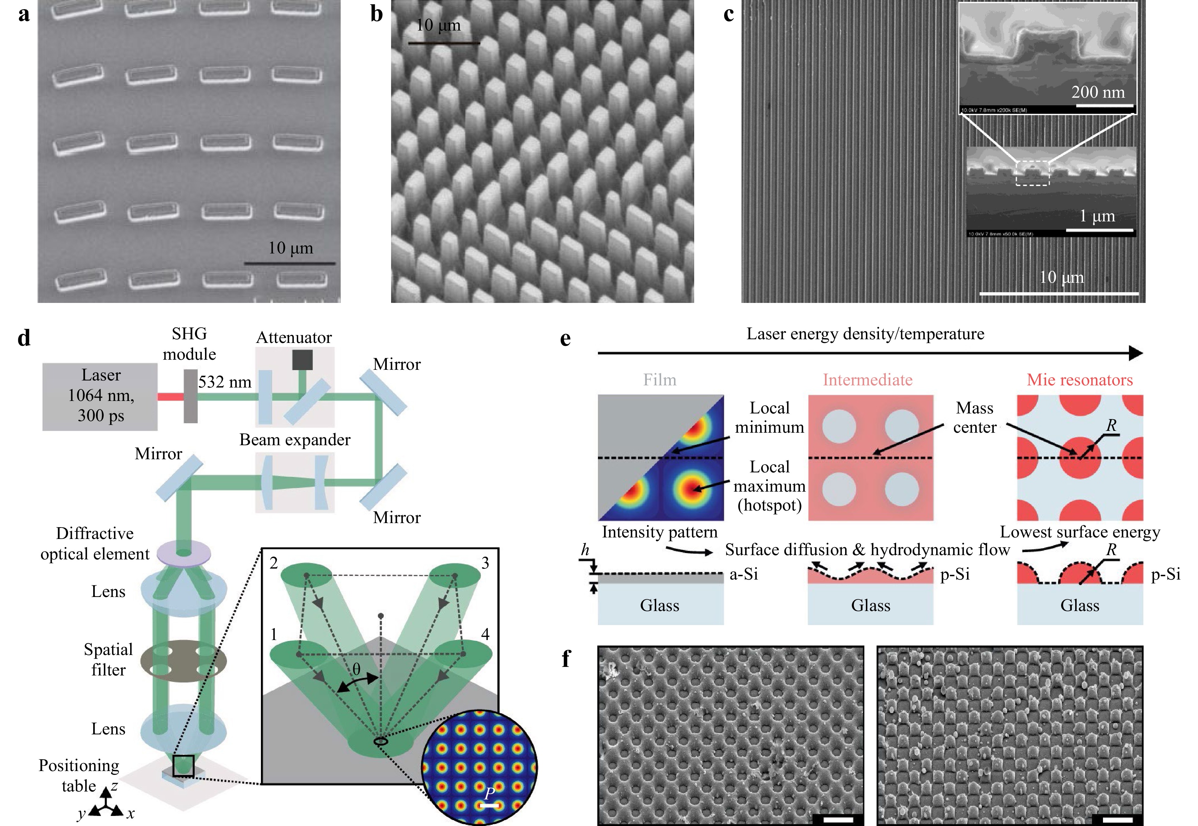
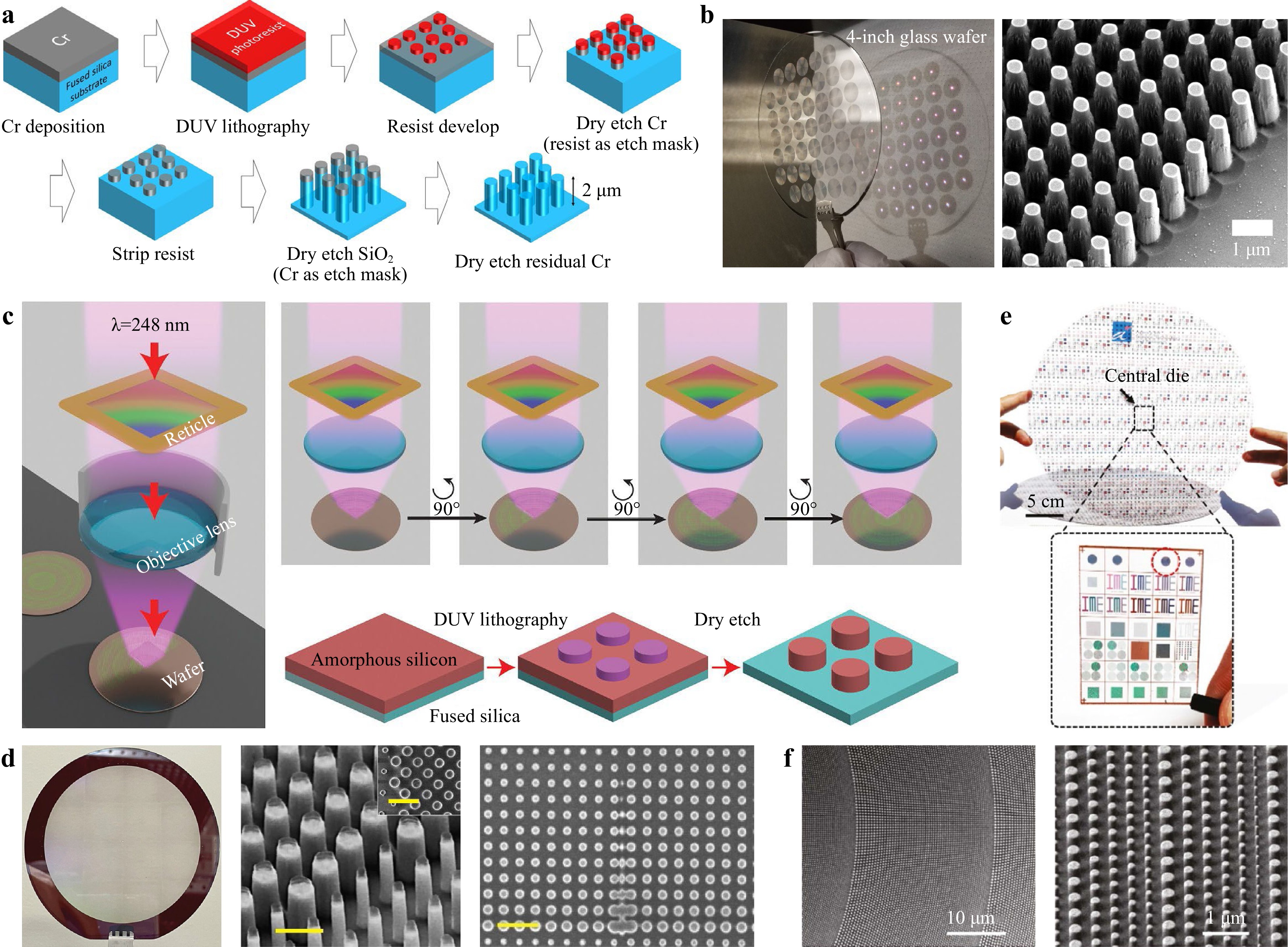
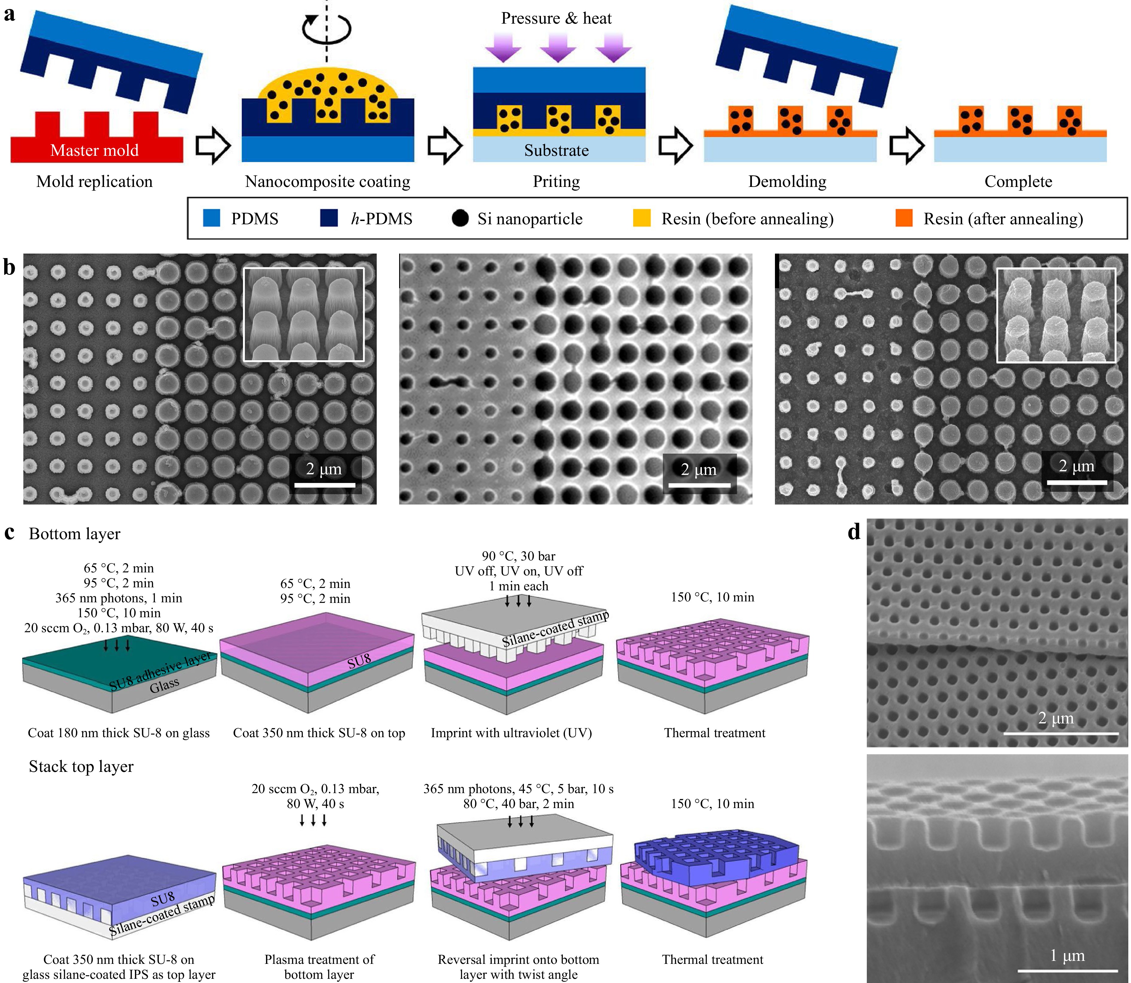
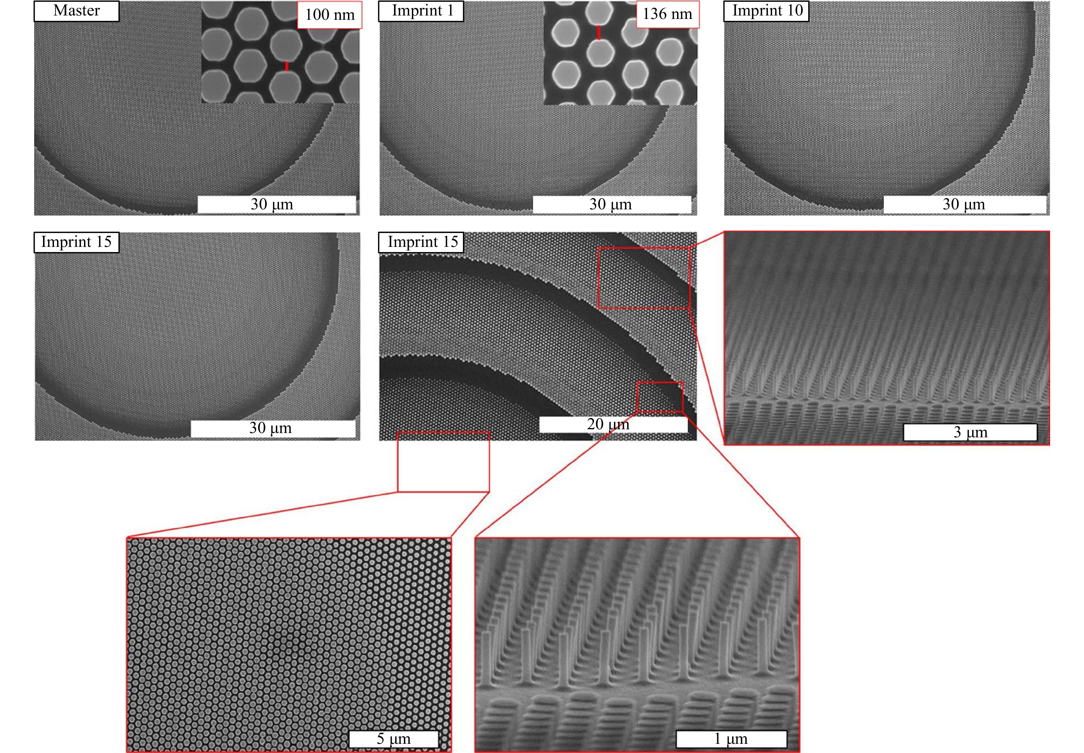
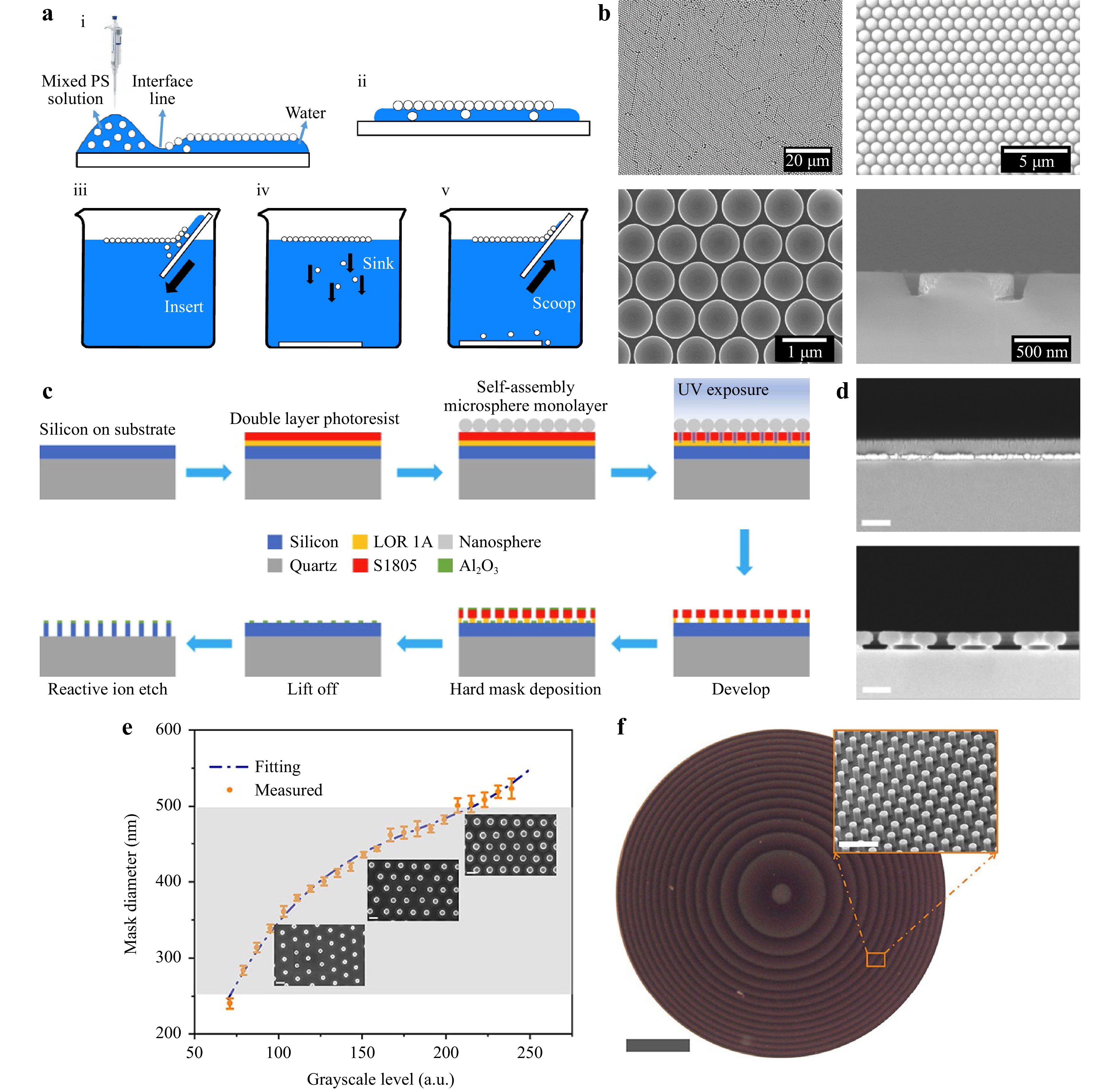
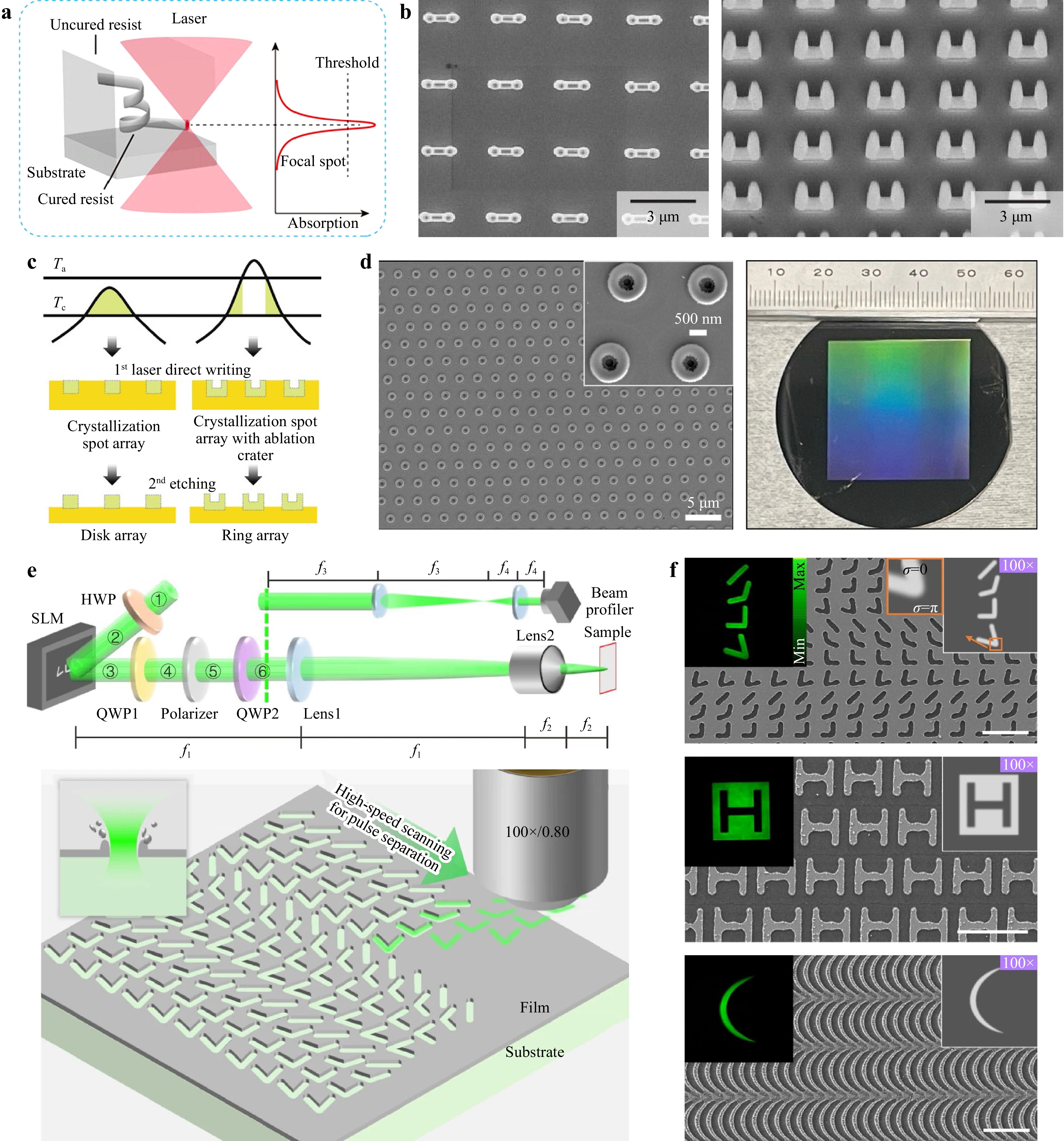
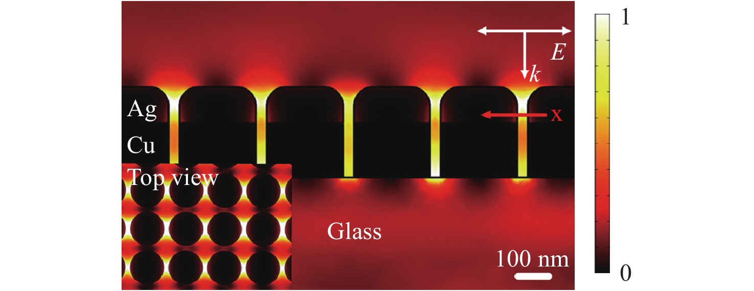
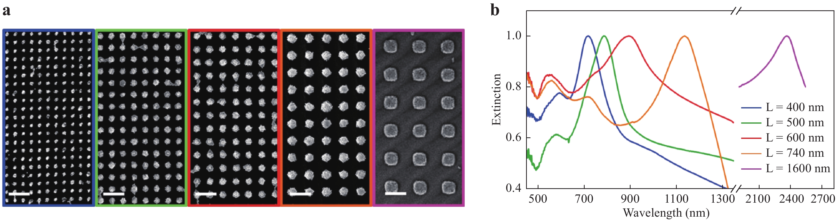
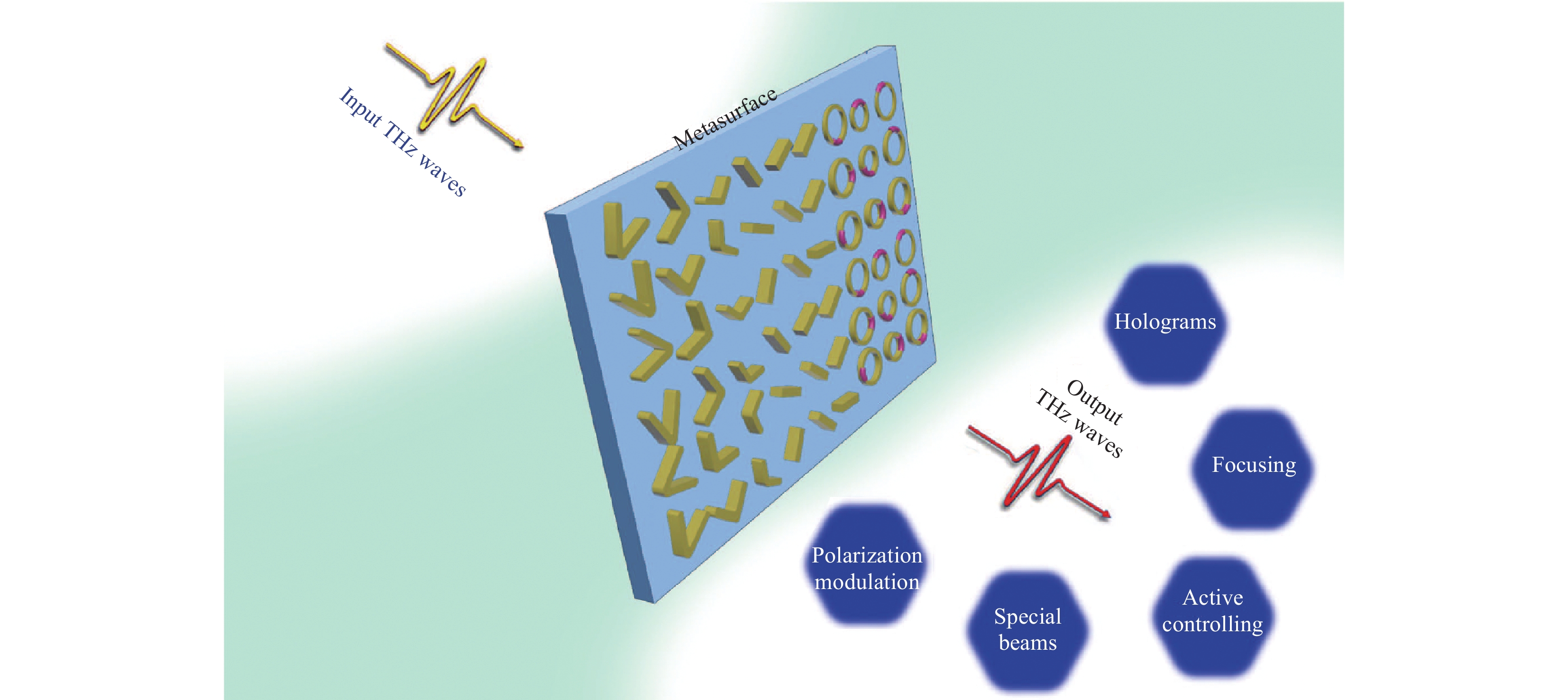
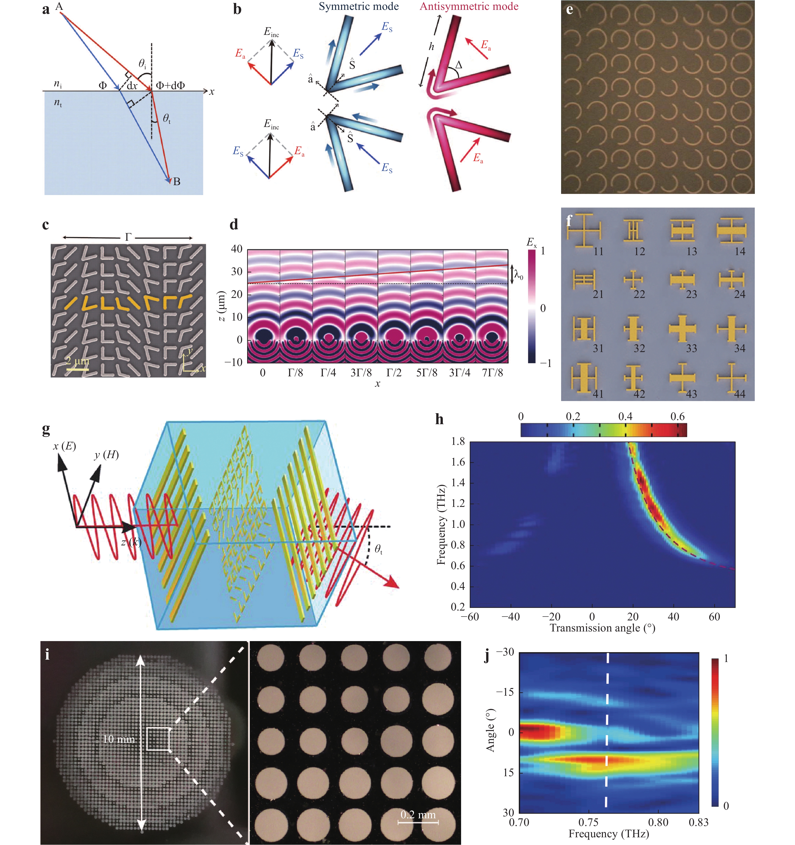
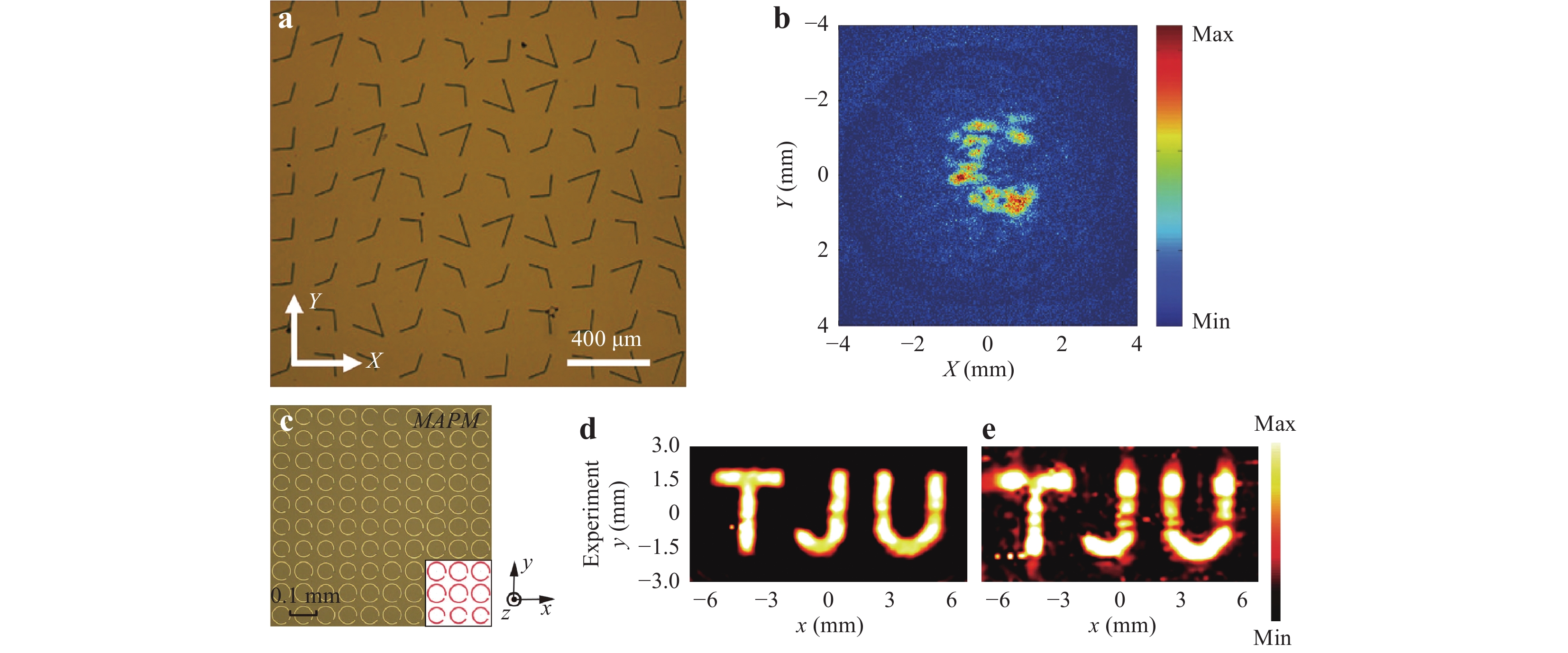
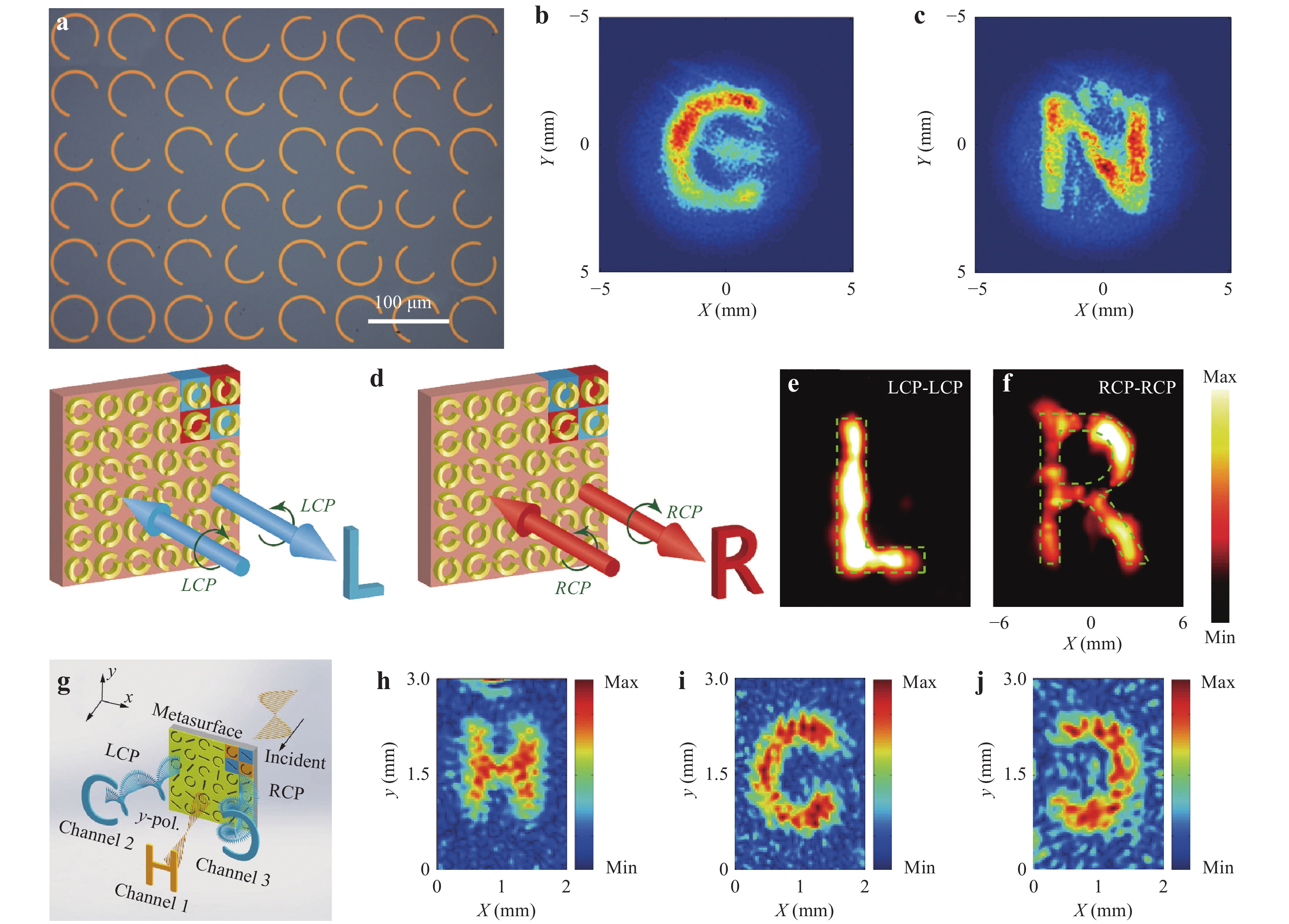
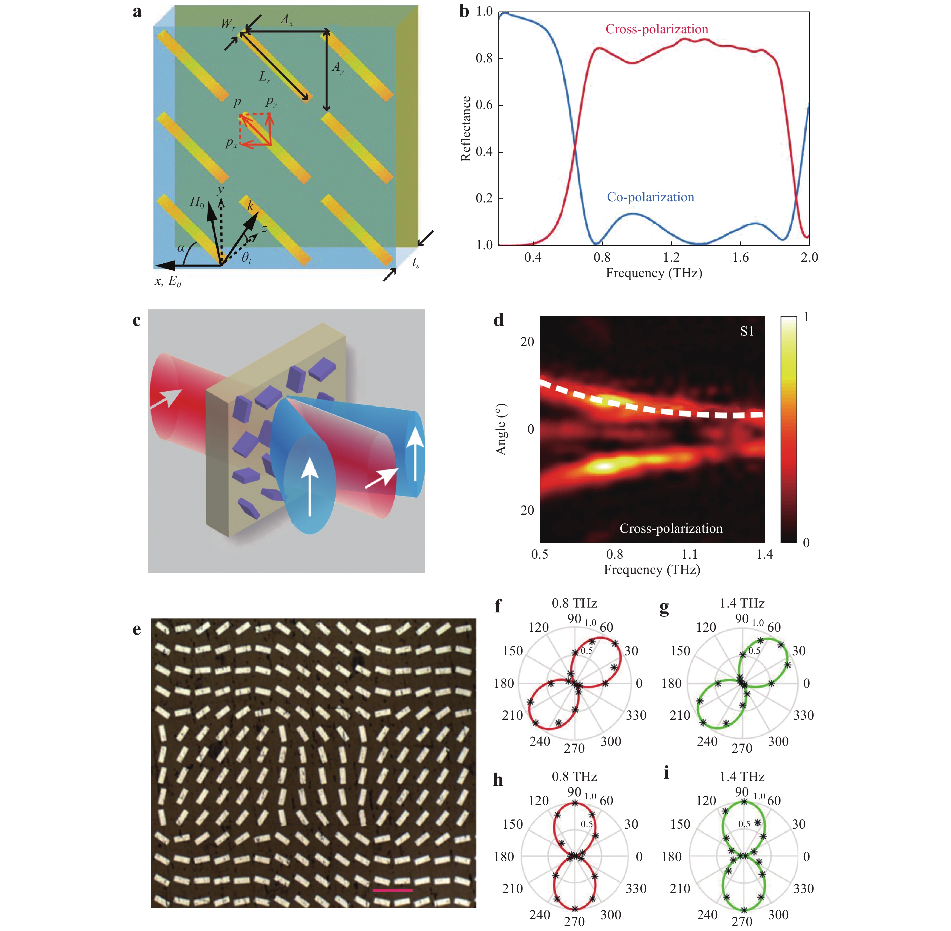
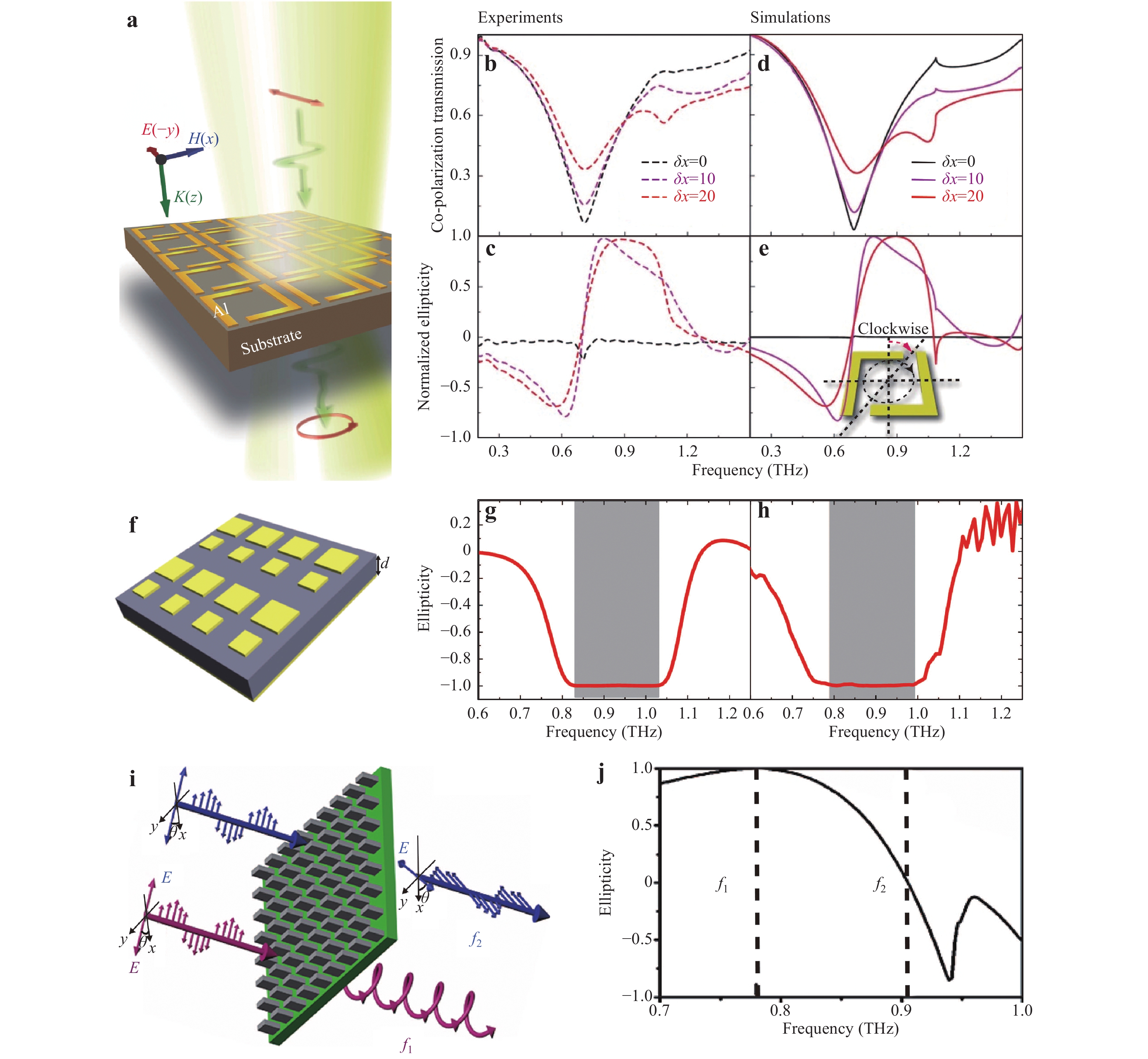
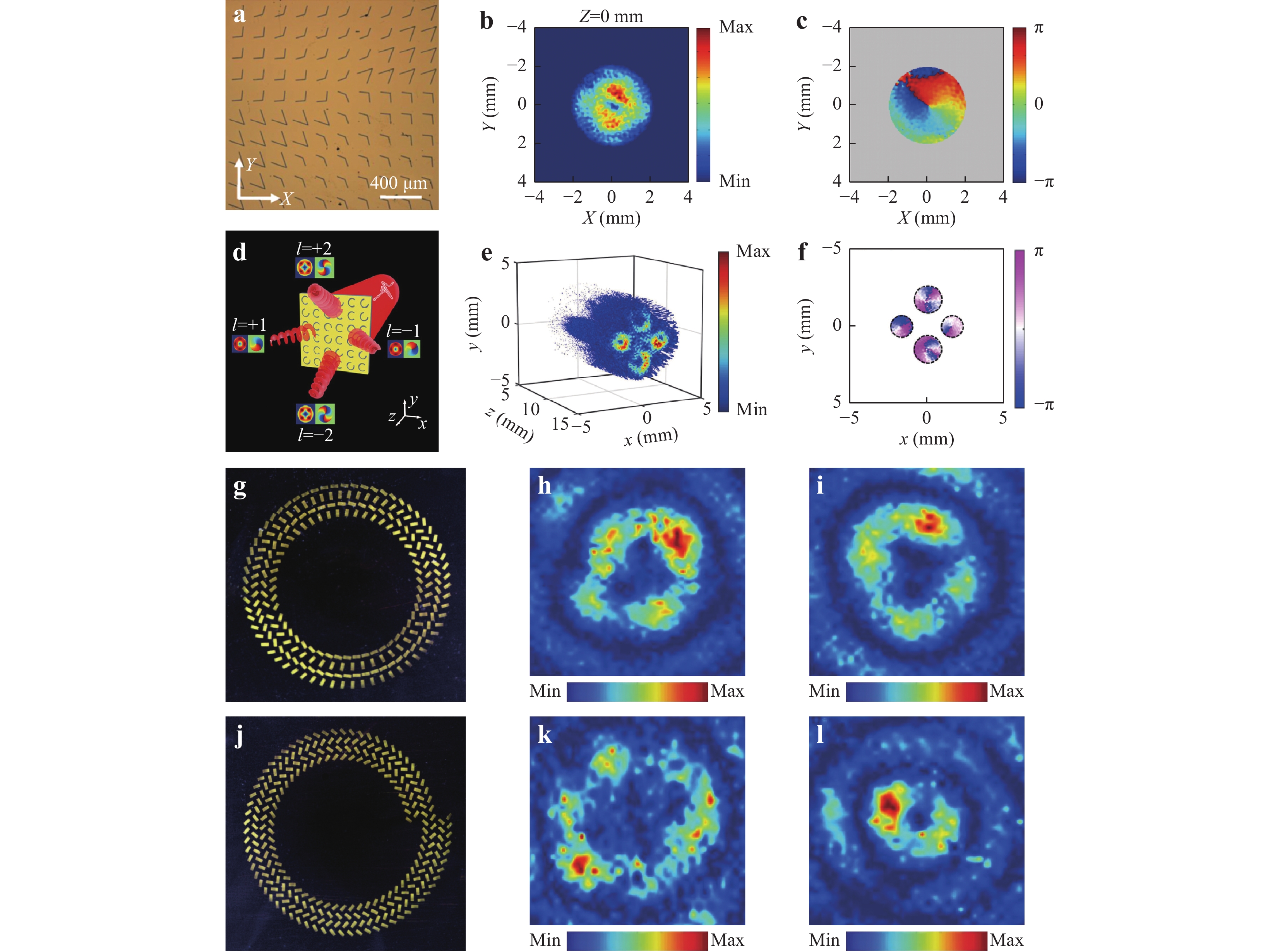
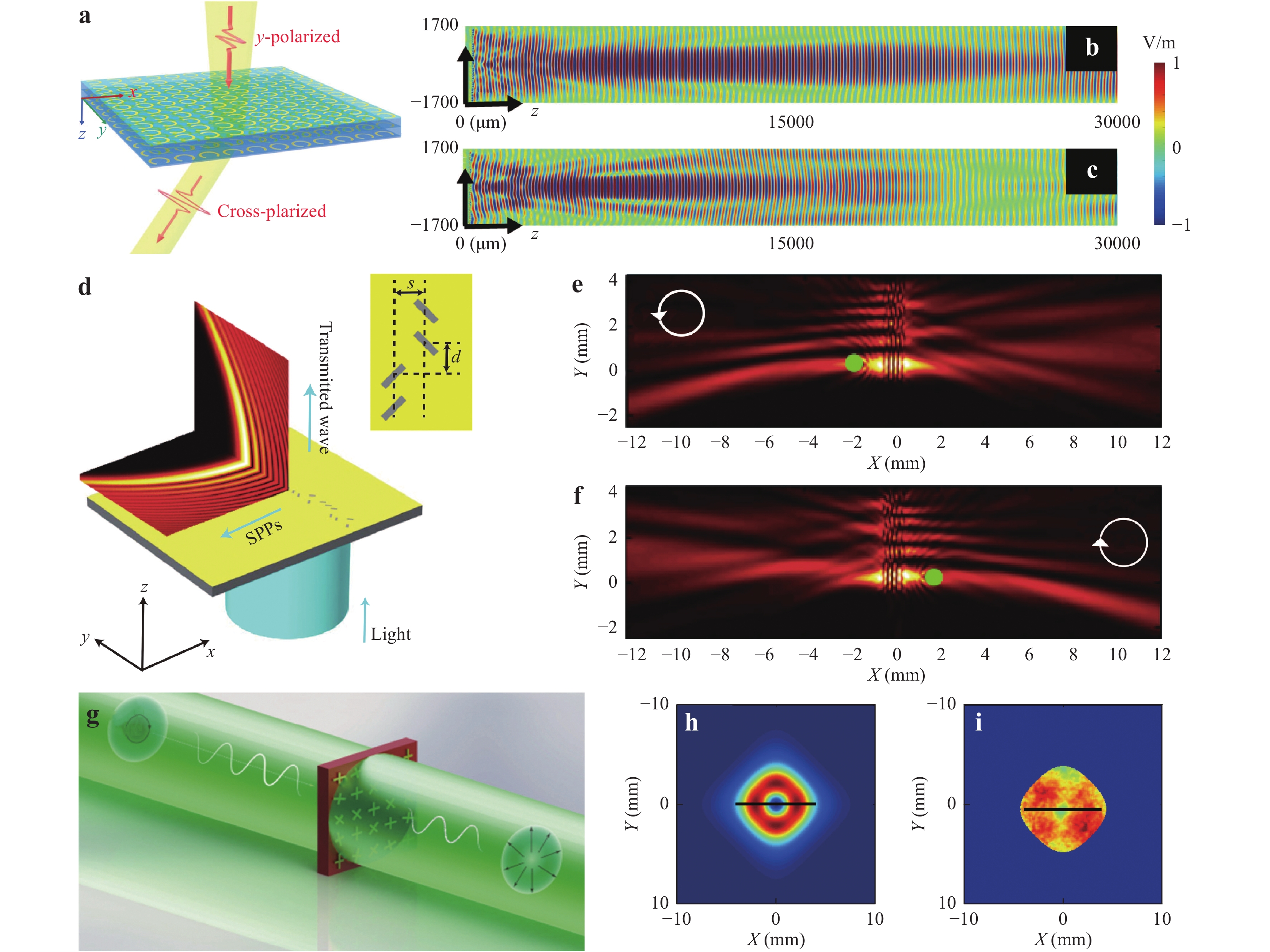
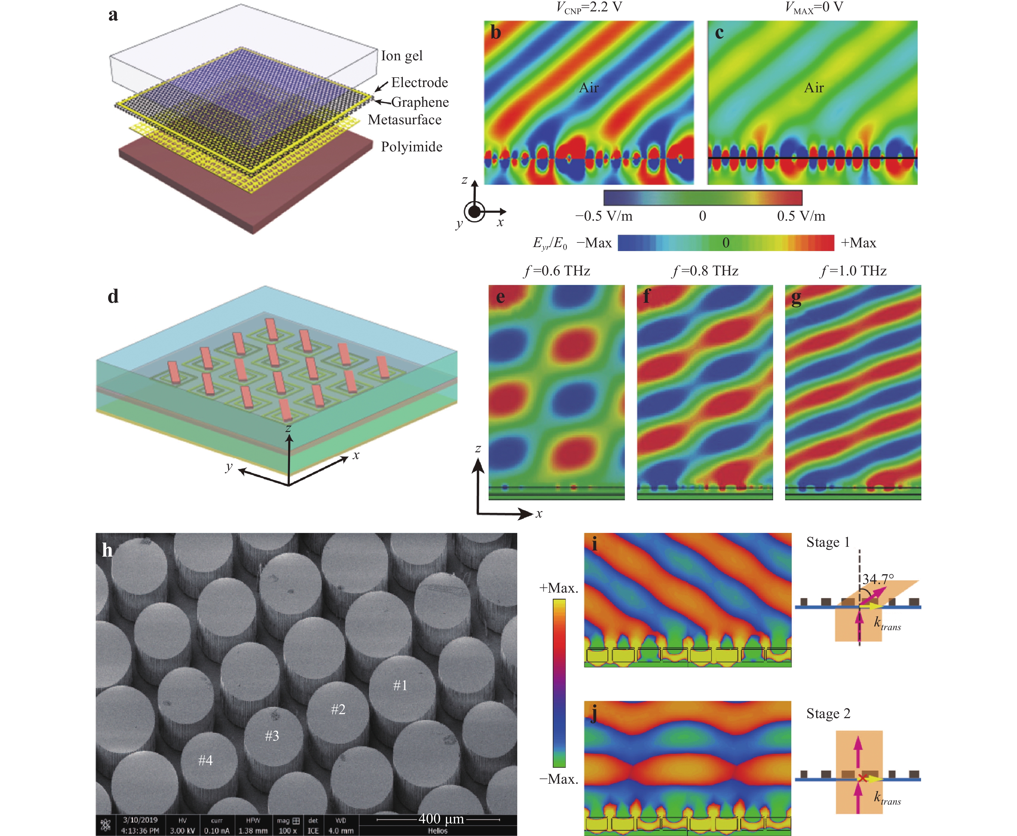
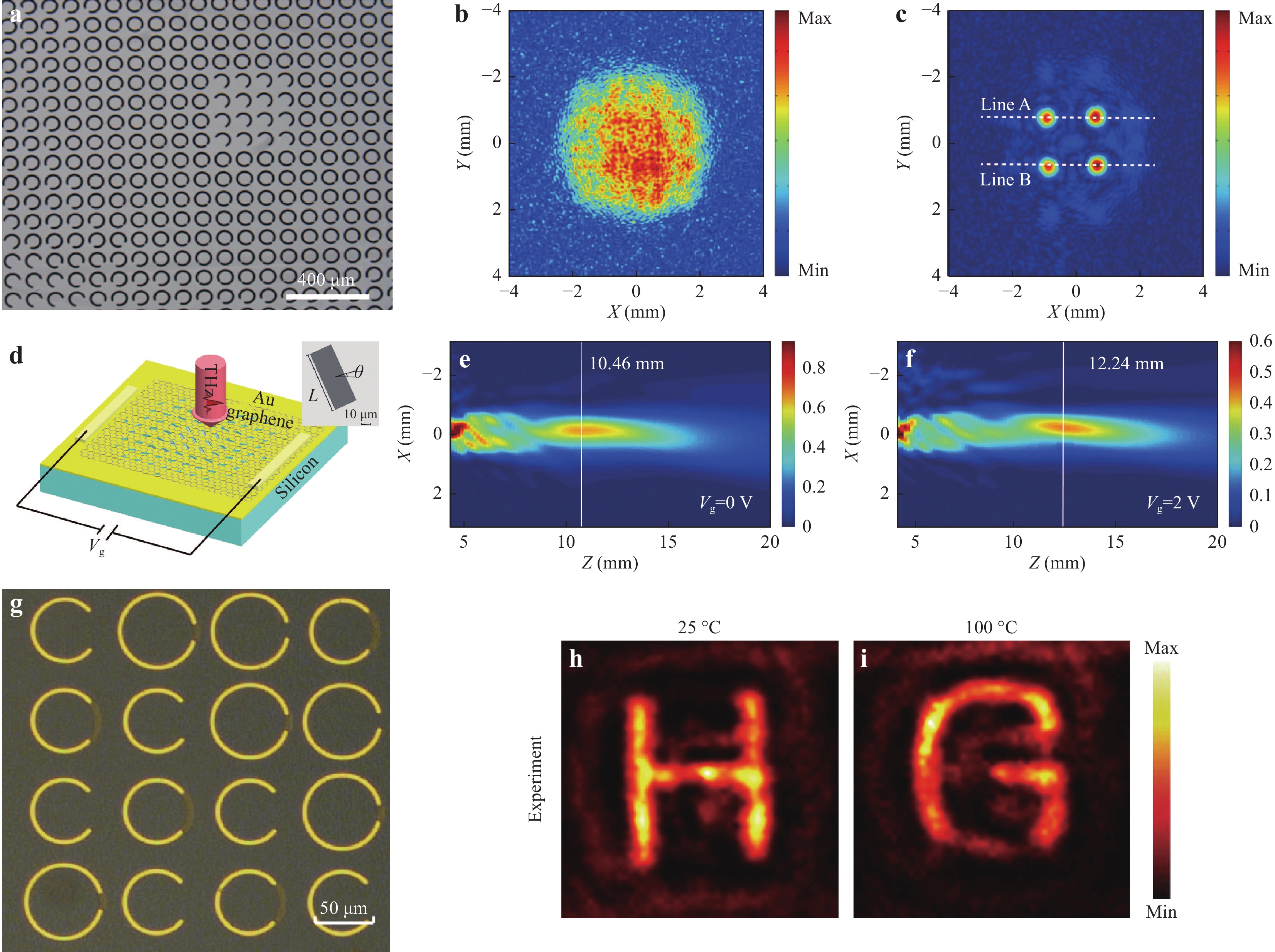
Metasurfaces are one of the most promising devices to break through the limitations of bulky optical components. By offering a new method of light manipulation based on the light-matter interaction in subwavelength nanostructures, metasurfaces enable the efficient manipulation of the amplitude, phase, polarization, and frequency of light and derive a series of possibilities for important applications. However, one key challenge for the realization of applications for meta-devices is how to fabricate large-scale, uniform nanostructures with high resolution. In this review, we review the state-of-the-art nanofabrication techniques compatible with the manufacture of meta-devices. Maskless lithography, masked lithography, and other nanofabrication techniques are highlighted in detail. We also delve into the constraints and limitations of the current fabrication methods while providing some insights on solutions to overcome these challenges for advanced nanophotonic applications.


 Email
Email RSS
RSS