


HTML
-
Surface-emitting lasers (SELs) operating at 1.3-μm are key devices for optical interconnects1, 2 spanning distances exceeding kilometers in length, and are crucial for low-cost high-capacity optical interconnects between data centers due to advantages including ease of testing and integration, low fabrication cost, and good beam quality with a circular beam. Several gain media emit at 1.3-μm. GaAs-based materials show more advantages than InP-based materials due to growth compatibility with AlGaAs/GaAs Bragg reflectors. Furthermore, compared with GaAs-based quantum wells (QWs)3, 4, In(Ga)As/GaAs quantum dots (QDs)5-11 are more promising because of the 3D carrier confinement, demonstrated low-threshold current densities and high characteristic temperatures12-14. Hence, 1.3-μm QD SELs are ideal candidates for long-distance optical interconnects.
SELs can be realized with vertical-cavity surface-emitting lasers (VCSELs) grown on a microcavity of an integer number of half-wavelengths using distributed Bragg reflectors (DBRs)5-9. However, the output power of 1.3-μm QD VCSELs under continuous-wave (CW) operation at room-temperature (RT) is at most 2.2 mW7, because of the complex and critical doping, growth of the DBR, oxide-confined structure, and hence poor thermal resistance. Although high power VCSELs with large apertures can be obtained, the higher-order modes resulting from the larger cavity critically degrade the beam quality.
Photonic-crystal surface-emitting lasers (PCSELs), which are based on band-edge effects of the photonic crystal (PC), realize self-mode locking (SML) by diffraction11, 15-22. The strong loss dispersion at the Brillouin zone center in PCs enables single-mode PCSELs with a large area22. Although, PCSELs can be viewed as a variation of grating coupled SELs10, 23, the multidirectional Bragg diffraction in PCSELs can yield coupling mechanisms unattainable with grating-coupled SELs, leading to control of the lasing mode over a large 2D area. In addition, the polarization17, beam pattern18, and direction19 of PCSELs can also be controlled. In contrast to VCSELs, surface emission is realized by PC diffraction, thus, no DBR is needed, which is especially suitable for 1.3-μm SELs. However, the power of 1.3-μm QD PCSELs is still limited to 2 mW when operated in pulsed mode at RT11.
PCs form energy bands for photons, which is an important attribute for PCSELs. A perfect or partial flat band is a dispersionless band structure24-26. Such a feature can provide slow light with zero group velocity and a high density of states over a broad range of the Brillouin zone. Therefore, enhanced light–matter interactions can be realized in such a range where a flat band exists27. In a previous study, a flat band was only realized at the second-order Gamma point, where a flat band mode exists and can support lasing of PCSELs28.
Inspired by the above works, in this study, the flat band of a PC is engineered to realize a high power 1.3-μm InAs QD PCSEL. In addition, an extra lateral feedback mechanism is introduced to further improve the output power of the PCSEL. The CW output power of the PCSEL at RT is 13.3 mW, which is higher than the output reported for any other 1.3-μm InAs QD SEL. Furthermore, such lasers can be operated at high temperatures, meeting the demands of optical communication applications.
A schematic of the structure of the PCSEL and its cross-section are shown in Fig. 1a, b, respectively. Light traveling in the slab is diffracted along the slab surface normal direction by the PC, forming a surface-emitting laser. Different from previous PCSELs, here we introduce a waveguide to form a Fabry–Pérot (FP) cavity, which can provide extra lateral feedback and a large area for current injection. The device width, length, and depth are 280, 800, and 2 μm, respectively.
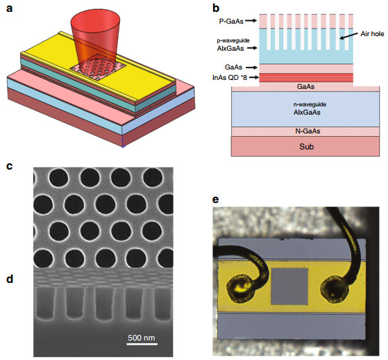
Fig. 1 Schematic drawing and optical micrograph of the PCSEL and SEM images of a PC.
a Schematic of the PCSEL. b Cross-sectional schematic of the PCSEL. c Top-view SEM image of the 2D PC. d Side-view SEM image of the 2D PC. e Top-view optical micrograph of the PCSEL.The PC region is 200 × 200 μm2, consisting of a triangular lattice in which each lattice point corresponds to a hole with a circular cross-section. Top-view and side-view scanning electron microscopy (SEM) images of the PC are shown in Fig. 1c, d, respectively. The lattice constant of the PC structure a is 520 nm. The diameter and depth of the holes are 300 and 800 nm, respectively. The holes were fabricated above the active layer, which favors realization of a high output power29. An overview top-view optical micrograph of the PCSEL is shown in Fig. 1e.
We calculate the transverse-electric (TE) band structure of the PC as shown in Fig. 2a, and then the band structure around the second-order Γ-point (Γ2) as shown in Fig. 2b. It is known that the mode with the highest Q value is favored for lasing. Thus the Q factor of each mode is calculated (Table S1 of the Supplementary Information), and it is found that mode B has the largest Q factor near the Γ2 Point. Therefore, mode B is more likely than the other modes to become the lasing mode. As shown in Fig. 2b mode B exhibits a flat band around Γ2 (between B1 and B2). In this flat band region, the group velocity of light becomes zero and a standing wave is formed. Such an unusual PC band structure is quite different from that of previous studies, in which the flat band only exists at Γ228. As a result, strong interaction between light and matter occurs not only at Γ2, but also in the vicinity of the flat band, which is the main factor for realizing a high output power of the PCSEL.
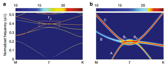
Fig. 2 Calculated TE band structure of the 2D PC.
a TE band structure of the 2D PC. b TE band structure of the 2D PC in the vicinity of the Γ2 point.We next discuss the lasing characteristics of our PCSEL under pulsed operation from 20 to 90 ℃. Under these conditions, thermal effects can be suppressed. We show the light–current characteristics for varying temperatures in Fig. 3. The maximum output power of the PCSEL is 150 mW at a current of 4.5 A, at 20 ℃ (RT). Under these conditions, the threshold current Ith and slope efficiency are 0.86 A and 40.9 mW A-1, respectively. As the operating temperature is increased, the output power and the slope efficiency of the laser decrease, and the threshold of the laser increases. It should be noted that the change in the light-current curves in the temperature range of 60–90 ℃ is larger than that in the temperature range 20–50 ℃.
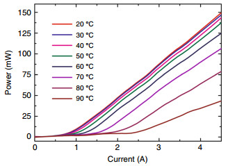
Fig. 3 Laser characteristics of the PCSEL under pulsed operation.
Light-current characteristics for temperatures from 20 to 90 ℃ for a drive current modulated at 5-kHz with a pulse duration of 2 μs.Next, the lasing characteristics of the PCSEL under CW operation are discussed. The measured output power of our PCSEL as a function of the injection current for various operating temperatures is shown in Fig. 4a. When the operating temperature is 20 ℃ (RT), the light-current curve exhibited thermal roll-over characteristics. The maximum output power of the device is 13.3 mW at 3.2 A, which is five times larger than that of previously reported InAs QD SELs7, 10, 11. The threshold current is 0.71 A, corresponding to a current density threshold of 48.2 mA cm-2 per layer of QDs. The slope efficiency of the laser is 5.8 mW A-1. With increasing operating temperature, the saturated output power and the slope efficiency decrease, and the threshold increases. However, when the temperature exceeds 70 ℃, the laser stops working normally due to thermal effects. Furthermore, in Fig. 4b we show the impact of the operating temperature on the threshold current Ith. From this curve one can calculate the characteristic temperature T0 of the PCSEL (Section 5 of the Supplementary Information), that is, 187 K in the range of 0–20 and 34 K in the range of 30–50 K.
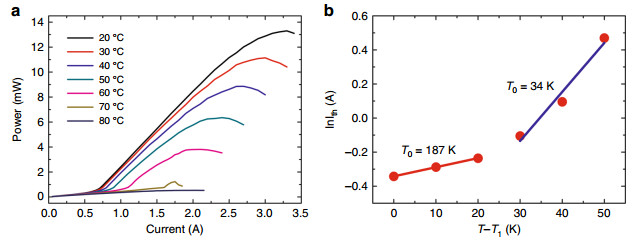
Fig. 4 Laser characteristics of the PCSEL for CW operation.
a Light-current characteristics for varying temperatures from 20 to 80 ℃ in steps of 10 ℃. b The characteristic temperature as a function of the threshold current Ith of the PCSEL.Last, we measure the spectrum of the PCSEL operating in CW mode at RT. As shown in Fig. 5a, the FP laser without a PC structure exhibits multimode output, while the PCSEL exhibits single mode output for both surface and edge emission. This phenomenon occurs because the PC can modulate the modes, suppressing the comb modes of the FP cavity and enhancing the PC mode around the Γ2 band edge. The spectrum of the surface emission of the PCSEL under a current of 1.2 A is shown in Fig. 5b. It can be seen that the PCSEL exhibits single-mode emission. The center wavelength and full-width at half-maximum (FWHM) of the spectrum are 1300.06 and 0.03 nm, respectively. In addition, the side mode suppression ratio (SMSR) is 18 dB. However, under a higher current, the PCSEL will exhibit multimode operation.
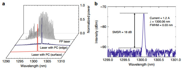
Fig. 5 Laser spectrum of the PCSEL operating CW at RT.
a The lasing spectrum of surface emission of the PCSEL (red line), edge emission of the PCSEL (blue line), and edge emission of the FP laser without a PC structure (gray line), respectively. b The spectrum of the surface-emitting PCSEL.In conclusion, we have achieved a 1.3-μm high power InAs QD PCSEL. We achieved an output power of 150 mW for pulsed operation at RT. The device can be operated in pulsed mode at temperatures up to 90 ℃. More importantly, we achieved an output power of 13.3 mW for CW operation at RT. This output power is five times larger than of that of previous InAs QD SELs. The device can be operated in CW mode at temperatures up to 60 ℃. The higher output power of the PCSEL occurs because of the flat band of the PC slab in the Brillouin zone and the introduced waveguide. Our fabrication process is simplified, reducing costs, because the need for DBR growth, epitaxial regrowth, and wafer fusion bonding is eliminated. Our devices provide a route towards realizing high-power 1.3-μm SELs that can be widely used in optical communications and for optical interconnects in super computers and data centers.
-
Using molecular beam epitaxy (MBE), layers were grown on an n-type GaAs (001) substrate. The details of the structure of the resulting QD sample are provided in Section 1 of the Supplementary Information.
The PC structure was fabricated on the QD sample. After depositing a 300-nm SiO2 etching mask by plasma-enhanced chemical vapor deposition (PECVD), a 2D PC was fabricated via electron-beam lithography followed by two ICP dry etching steps.
After fabrication of the PC structure, the PCSEL was fabricated by the conventional edge-emitting-laser fabrication process. The samples with a PC structure were patterned into stripe lasers by photolithography and ICP dry etching. A 200-nm thick SiO2 electrical insulating layer was deposited by PECVD at 300 ℃, and a contact window opening was fabricated within the PC area by photolithography and ICP dry etching. Standard p-side metallization was performed via a lift-off process, and finally, after the processes of substrate thinning and metallization of the n-side, a single device was obtained.
-
Simulations were performed by the finite-difference time-domain (FDTD) method to investigate the band structure of the PC slab. Here, only TE modes were focused on, because the gain of the TE mode is larger than the gain of the transverse magnetic (TM) mode. The band structure around Γ2 was investigated at a higher resolution, because in the vicinity of Γ2, the PC will supply distributed feedback and couple the light into the normal direction.
-
The light-current characteristics were measured by a thermal-type power meter, which was placed in front of the PC area normal to the surface of the PCSEL. The temperature was controlled by thermoelectric cooling (TEC). The width and delay of the pulse were 2 μs and 20 ms, respectively.
The spectrum was measured at a current of 1.2 A, and the laser beam was collected by a single-mode fiber coupled to an optical spectrum analyzer (Yokogawa AQ6370C).
Fabrication
Simulation
Measurement
-
This work was supported in part by the National Science Foundation of China (61774156 and 61761136009), in part by the National Key Research and Development Project (2018YFB2201001), in part by the External Cooperation Program of the Chinese Academy of Sciences (181722KYSB20160005), in part by the Jilin Provincial Natural Science Foundation (20180519024JH) and in part by the Youth Innovation Promotion Association of the Chinese Academy of Sciences (2018249).
-
H.Y.L. and C.Z.T. designed the structure, H.Y.L. and S.C.T. performed the fabrication. S.L.S. packaged the devices. H.Y.L., L.J.W., J.M.R., C.Y.L., and H.W. performed the measurements. S.C.T. and H.Y.L. prepared the original draft, C.Z. T. revised the manuscript. S.C.T. and C.Z.T. provide the funding. All authors discussed the results.
-
The authors declare that they have no conflict of interest.
-
Supplementary information is available for this paper at https://doi.org/10.1038/s41377-019-0214-2.

 DownLoad: