


-
Quantum dot (QD) light-emitting diodes (QLEDs), owing to their tunable emission spectra, wide colour gamut, and high electroluminescence efficiency, are widely recognized as strong candidates for next-generation display technologies1–5. To deliver vivid and realistic images and provide an immersive visual experience, display resolution must approach the perceptual limits of human vision. This typically demands pixel densities of several hundred pixels per inch (PPI), with even higher values required for near-eye display applications6–8. Therefore, QDs must be patterned with microscale precision to satisfy these stringent resolution requirements. Various fabrication approaches, including inkjet printing9–13, transfer printing14–18, and photolithography8,19–22, have been investigated for high-resolution QD patterning; however, each method suffers from intrinsic limitations that restrict their broad applicability. For example, inkjet printing encounters significant challenges in forming QD pixels with dimensions below a few micrometers23,24, whereas transfer printing often suffers from alignment difficulties at the microscale, resulting in reduced fidelity of high-resolution QD patterns25. Conventional photolithography, by contrast, relies on photoresists that hinder the formation of uniform QD thin films and impede efficient charge injection19,26. Furthermore, the high-dose deep ultraviolet (DUV) exposure required in this process can significantly degrade QD performance20,27,28. Consequently, the development of innovative techniques capable of achieving enhanced resolution while maintaining the optical and electrical integrity of QDs has emerged as a key focus in the advancement of QD display technologies.
Direct photolithography holds significant promise as a nondestructive, high-resolution, and high-yield technique for QD patterning21,29,30. By eliminating the need for photoresists, it simplifies the fabrication process, prevents undesirable interactions between photoresists and QDs, and minimizes the detrimental effects of etching on device performance. This approach also facilitates uniform QD deposition on the substrate, enabling the formation of high-resolution patterns. The principle of direct photolithography is based on the photosensitivity of QDs, combined with a photo-crosslinker. Upon exposure, the mixture of QDs and photosensitive compounds undergoes photochemical reactions, producing a pronounced solubility contrast between exposed and unexposed regions. This contrast allows the selective removal of more soluble regions using a developer, thereby forming the desired QD patterns22,27,31. Nonetheless, even the most advanced crosslinkers cannot entirely prevent photodamage to the luminescence properties of QDs during photolithography32–34. To improve crosslinking efficiency, DUV irradiation at 254 nm is commonly employed. However, this high-energy DUV exposure inevitably damages the QD surface, resulting in the creation of trap states. Consequently, the photoluminescence quantum yield (PLQY) of the QDs is markedly reduced, adversely affecting both pattern fidelity and overall device performance33,35.
In this article published in Light: Science & Applications, Chen et al. reported a direct photolithography strategy employing a rigid crosslinker, demonstrating its significant potential for producing nondestructive, high-quality, and high-resolution patterned QD layers36, as illustrated in Fig. 1. The authors designed a crosslinker incorporating a rigid cyclopentane (CPT) bridging group, which demonstrates strong UV absorption and substantially reduces the energy threshold required for the photo-crosslinking reaction. Furthermore, the restricted rotation imparted by the CPT unit results in a pronounced decrease in the solubility of QDs following crosslinking. Consequently, the required DUV dose is markedly reduced, allowing efficient and nondestructive patterning of QD films. The study demonstrated pixelated RGB arrays with an impressive resolution of 6350 PPI. In addition, it presented a gradient line pattern on a substrate, where the pixel width gradually varied from 3 to 1 μm, exemplifying the capability of direct photolithography to flexibly and precisely control pixel linewidth. This provides a solid foundation for fabricating optoelectronic devices with functional gradients. More importantly, beyond applications on rigid substrates, the study also demonstrated successful QD patterning on flexible substrates such as polyethylene terephthalate (PET), highlighting its potential for the development of flexible and wearable display devices—a significant step toward next-generation electronics. Furthermore, the electronic energy level of the crosslinker plays a key role in preserving and even enhancing the PL performance of patterned QD layers. The authors ascribed this improvement to the rigid architecture of the crosslinker, which limits electron delocalisation and consequently elevates the energy of the lowest unoccupied molecular orbital (LUMO). A higher LUMO level establishes a stronger energetic barrier for excited electrons in QDs, effectively preventing carrier trapping and suppressing non-radiative recombination following light absorption. Additionally, the crosslinker contributes to surface defect passivation in the QDs. As a result, the patterned QDs retain 99% of the PLQY of pristine QDs. To directly evaluate the device performance, the authors compared the electroluminescent (EL) characteristics of pristine and patterned red QLEDs. Both devices demonstrated excellent performance, with the patterned devices maintaining 96% of the external quantum efficiency (EQE) and 98% of the current efficiency relative to the pristine devices. These findings strongly highlight the nondestructive nature of the direct photolithography process.
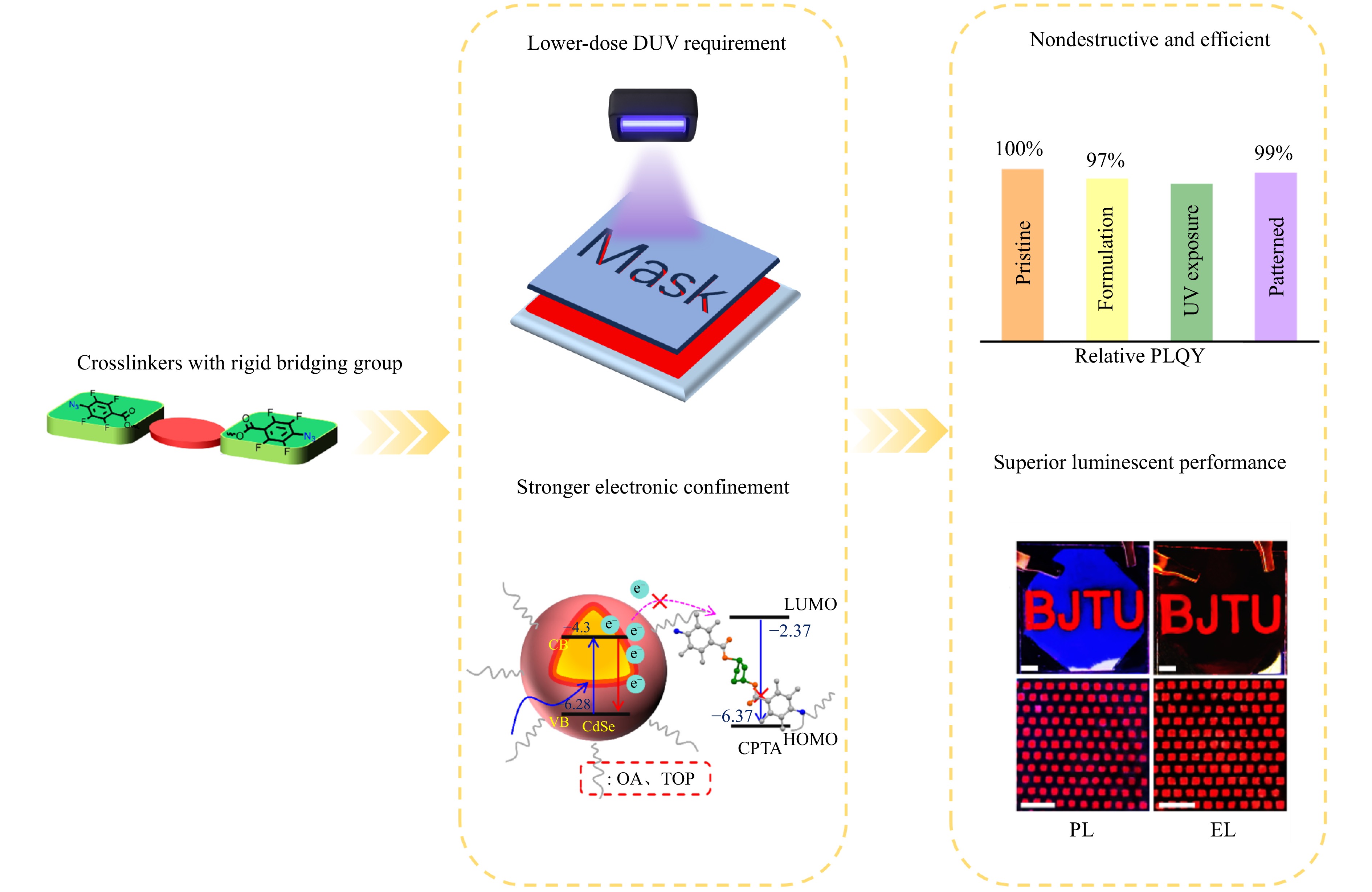
Fig. 1 Schematic of nondestructive, high-quality, high-resolution QD patterning facilitated by a rigid crosslinker. (Left) Structure of the rigid crosslinker. (Middle) Advantages of using rigid crosslinkers in direct photolithography processes. (Right) Nondestructive effects of rigid crosslinkers on QD thin films during direct photolithography, and the demonstration of the resultant device luminescence. Some images are reproduced from Ref. 36.
This work demonstrates that the rational design of a rigid crosslinker can effectively overcome key limitations in the direct photolithography of QLEDs. It enables nearly nondestructive, high-quality, and high-resolution patterning of QD films, paving the way for the development of high-resolution, high-efficiency QLEDs suitable for next-generation immersive display technologies.
Notably, the patterning of RGB QLED arrays is a crucial step toward achieving full-colour displays. In multiple photolithographic cycles, repeated deposition, exposure, and development steps can adversely impact the pre-defined QD regions8,20,37. Therefore, it is essential to evaluate the optical and electrical performance of patterned QD films following multiple photolithography steps. Although the proposed direct photolithography strategy shows strong potential for monochromatic QLED arrays and current single-color display applications, its scalability and applicability to full-colour, high-resolution displays require further investigation.
Finally, innovations in patterned QLED technology may significantly accelerate the integration of QLEDs into microdisplay applications. Compared with OLEDs, QLEDs offer superior colour purity, higher brightness limits, and greater compatibility with scalable patterning techniques, making them particularly well-suited for augmented and virtual reality (AR/VR) displays, where ultra-high resolution and luminance are critical38–40. With ongoing progress in high-precision patterning, QLEDs are now capable of producing micron-scale full-colour arrays, paving the way for the mass manufacture of high-PPI microdisplays21,24,41,42. Looking ahead, QLEDs are strategically poised to spearhead the next generation of innovation in microdisplay technologies, potentially transforming the landscape of the display industry.
High-resolution, nondestructive patterning of quantum dots via rigid crosslinker-enabled direct photolithography
- Light: Advanced Manufacturing , Article number: (2025)
- Received: 25 July 2025
- Revised: 20 October 2025
- Accepted: 21 October 2025 Published online: 12 November 2025
doi: https://doi.org/10.37188/lam.2025.081
Abstract: A direct photolithography approach using rigid crosslinkers was developed for the precise patterning of quantum dot (QD) layers, producing high-resolution RGB arrays with pixel sizes down to 1 μm. This strategy suppresses QD degradation typically associated with conventional high-UV photolithography while enhancing electron confinement within the QDs, thereby preserving their luminescent properties. As a result, high-performance patterned red QLEDs were successfully fabricated.
Rights and permissions
Open Access This article is licensed under a Creative Commons Attribution 4.0 International License, which permits use, sharing, adaptation, distribution and reproduction in any medium or format, as long as you give appropriate credit to the original author(s) and the source, provide a link to the Creative Commons license, and indicate if changes were made. The images or other third party material in this article are included in the article′s Creative Commons license, unless indicated otherwise in a credit line to the material. If material is not included in the article′s Creative Commons license and your intended use is not permitted by statutory regulation or exceeds the permitted use, you will need to obtain permission directly from the copyright holder. To view a copy of this license, visit http://creativecommons.org/licenses/by/4.0/.

 DownLoad: