


-
Recently, the introduction of nonlinear optical functions in integrated optics has sparked a lot of enthusiasm. Demonstrations (such as frequency combs1–4, supercontinuum sources5–7 suited for scientific and industrial applications, and photon pairs sources for quantum applications8–10) have shown the potential for integrated photonic platforms. Furthermore, large-scale manufacturing capability and affordability have motivated the development of fully integrated, nonlinear optical devices, aiming at various applications, such as all on-chip spectroscopy11, on-chip quantum computations and communications12, efficient multiplexing for data communications13, on-chip metrology14, bio-sensing15,16, or LIDARs17.
Integrating these different active functions in silicon photonics18, has also attracted much attention. The possible compatibility with CMOS processes and the overall low cost of the platform indeed makes it very attractive to the industry, with devices directly suitable for dense optical circuit fabrication. These deep integration capabilities make the Si-compatible platform an interesting testbed for the transposition, on a miniaturized and integrated scale, of optical functions initially developed on more macroscopic scales by bringing together various cumbersome elements needing precise alignments. However, silicon photonics presents some impediments when considering the exploitation of nonlinear optical processes due to the weak nonlinear responses of the most common materials (i.e., SiO2, SiN) compatible with its clean room processes, or to the presence of free carriers around 1.5 µm wavelength. In this C-band range, Si is highly nonlinear but suffers from Two Photons Absorption (TPA) due to its low bandgap of ~ 1.12 eV (at room temperature). Unfortunately, as seen in Table 1, most of the classical materials compatible with silicon integration, e.g., SiO2 and SiN, lack strength in terms of optical nonlinearities. For instance, the stochiometric SiN nonlinear refractive index (n2) is almost two orders of magnitude lower than that of Si. Although SiN/SiO2 waveguides show great advantages in linear optics (e.g., a much lower index contrast than Si/SiO2 and low propagation loss (~ 3 dB/m19,20)), the stochiometric SiN nonlinear refractive index (n2) is almost two orders of magnitude lower than that of Si.
Material Integrated optics Free space n2/n2si
(n2si=7.2×10⁻¹⁸ m2·W−1)Refractive index
(at 1550 nm)TPA (at 1550 nm) [m·W−1] χ(3) (m2V−2) @
1550 nmχ(2) (m1V−1)
(emission wavelength)Band gap (eV) Si 121 3.5 0.5×10⁻¹¹ 1.6×10⁻²¹ − 1.12 Si3N4 0.034 5 1.9-2.0 None 2.3×10⁻²² − − SiO2 0.003 1.44 None − − − WS2 291.622 − 1.58×10⁻⁹ 2.4×10⁻¹⁹ 23 68×10−11 24(600 nm) 2.1 MoS2 37.525
15.2826− − 3.6×10⁻¹⁹ 23 2.9×10⁻¹¹ 27
(780 nm)2 WSe2 − − − 1.0×10⁻¹⁹ 23 0.4×10⁻¹¹ 28
(730 nm)1.75 MoSe2 − − − 2.2×10⁻¹⁹ 23 5×10⁻¹¹ 29
(640 nm – 700 nm)1.7 BP − − − 1.6×10⁻¹⁹ 30 − 0.3−2 Graphene 2.0831
5.6932
10.69 33
2.7834− −
1.0×10⁻¹⁹ 35− Zero-gap GO 1600-375036 − − − − − Table 1. Second- and third-order nonlinear optical parameters at the technically important telecom wavelengths for the most common 2D materials and the primary materials of the CMOS-compatible platform used in Si and Si-hybrid integration schemes. We distinguish the results obtained in integrated settings and free space, as shown by the discrepancies below. BP stands for black phosphorous, and GO for graphene oxide, n2Si is the value of the Kerr refractive index for Si at 1550 nm.
Yet, impressive demonstrations have been presented throughout the years using various silicon-based materials to generate integrated optical functions, such as supercontinuum sources5–7, frequency combs1–4, and photon pair sources through spontaneous four-wave mixing. As the application fields developed, the requirements became more demanding. In some fields, such as high-power computing or data communications, the communities have pushed for more efficient devices showing high performance with low power consumption. Annealed SiN waveguides with loss levels of few dB/m have been demonstrated (e.g., allowing the generation of octave-spanning supercontinuum processes5,6,37), yet the needed pump power was still large1,4,38. Moreover, long waveguides were needed to achieve sufficient nonlinear processes, thus making optical functions demanding for fully integrated devices.
Alternatively, materials such as Si-rich waveguides39–42 or the use of p-i-n junctions to engineer carrier density43 have shown some promising results but have some drawbacks. For instance, Si-rich waveguides still present TPA, while the use of multiple p-i-n junctions adds another layer of complexity to devices and circuits. Hence, the need for solutions to this limitation is still strong.
Another approach is to introduce highly nonlinear materials to the on-chip platform to take advantage of the highly effective properties of these materials, thus boosting their nonlinear performance via the integration strategy. Following that idea, several materials have been tested throughout the past decade. Chalcogenides are a popular alternative to Si-based materials (e.g., GaAs44, As2S345,46, GeSe47, GeSbS48 or GaS49). In the quest to identify disrupting nonlinear optical materials, two-dimensional (2D) layered materials have been identified as extremely promising23,25–27,31,50, for example, with third-order susceptibility up to two orders of magnitude higher than that of Si. The most widely known material in this category is graphene. Still, other 2D materials such as Transition Metal Dichalcogenide (TMDs, MX2 like crystals where M stands for a metal atom and X for a chalcogen like MoS2, WS2, WSe2, MoSe2) or BP are also receiving increasing attention51,52. The principle behind hybrid integration (Fig. 1) consists in incorporating high-performance 2D materials into the existing integration platforms, thus increasing the overall effective nonlinear performance of the waveguides. Yet, several challenges arise from the hybrid integration approach, as 2D materials are still not fully understood. The impact of their addition to integrated structures needs to be handled carefully (such as dispersion, mode distribution, and nonlinear optical responses). This review presents recent progress in the field and our perspectives after briefly introducing the theoretical background of the hybrid integration of 2D materials for the different integrated optics platforms. The aim is to describe key steps, from the modeling and the design to the characterization steps. This will hopefully serve as a guideline for future works on the related fields, thus solving one of the obstacles met with integrated nonlinear photonics.

Fig. 1 Conceptual representation of the hybrid integration of 2D materials. Below are lists of the most common 2D materials with their bandgaps that have been integrated with waveguide structures. The inset spectra show the input (red) spectrum, and the output broadened spectra (blue for intrinsic waveguides and green for the 2D material integrated waveguides) during a typical pulse broadening experiment.
-
There is more to consider designing a hybrid waveguide structure than a more common waveguide due to the properties of the added material to the structure and the waveguides. Among all the different design factors, engineering the optogeometrical structures of the hybrid waveguide is one of the key parts of designing integrated nonlinear optical functions. Therefore, it is essential to estimate through eigenmode calculation the waveguide properties on which they are based53. This mainly includes their effective index values, the transverse mode distributions, and the Group Velocity Dispersion (GVD) profiles at the operating wavelength. For 2D material integrated hybrid waveguides, the difficulty is to consider the modelling of a quasi-surface 2D material correctly. However, the induced optical effect of a 2D material, mainly reflected in its surface conductivity, can be significant. This important physical quantity can be, in fact, described in two different ways: either by using the bulk surface conductivity $ {\sigma }_{b} $ in which the 2D material (or their heterostructures) is considered as a bulk material with an atomically thin thickness or, using a real surface conductivity ($ {\sigma }_{s} $) approach accounting for the actual 2D nature of the material. The two different methods yield the same results. However, in the first case, a typical Finite Difference Eigenmodes (FDE) calculation may require a very tight mesh to properly account for the boundary conditions set by the hybrid structure (monolayer 2D materials having thickness revolving around 1 nm and the overall structure having a dimension in the order of a few µm). This is why 2D materials can be preferentially described in waveguide mode calculations by the second approach, which needs a proper $ {\sigma }_{s} $ estimation. Several methods exist to perform the estimation of this parameter54. For graphene, analytical solutions can be found. The Dirac-cone shape of its band structure indeed allows for analytical investigation55-57
$$ {\sigma }_{s}\left(\omega \right)=\frac{{e}^{2}{E}_{F}}{\pi {\hslash }^{2}}\frac{\tau }{1-i\omega \tau }+\theta (\hslash \omega -2{E}_{F})+\frac{i}{\pi }ln\left|\frac{\hslash \omega -2{E}_{F}}{\hslash \omega +2{E}_{F}}\right| $$ (1) with ω the frequency, e the elementary charge, $ \hslash $ the reduced Planck constant, EF the Fermi energy level, τ the relaxation time, and θ the Heaviside step-like function54. Surface conductivity for graphene can be calculated (EF = 0.6 eV and τ=0.25/2π) accordingly and is displayed in Fig. 2a. For other 2D materials, an analytical approach is not yet available due to their more complicated band structures. Hence, for 2D materials such as TMDs, experimental measurement data are required for the numerical modelling of the 2D materials (e.g., MoS2, WS2, MoSe2, WSe258). Fitting the data by a sum of Lorentzian, one can then calculate the relative permittivity $ {\varepsilon}_{r} $:
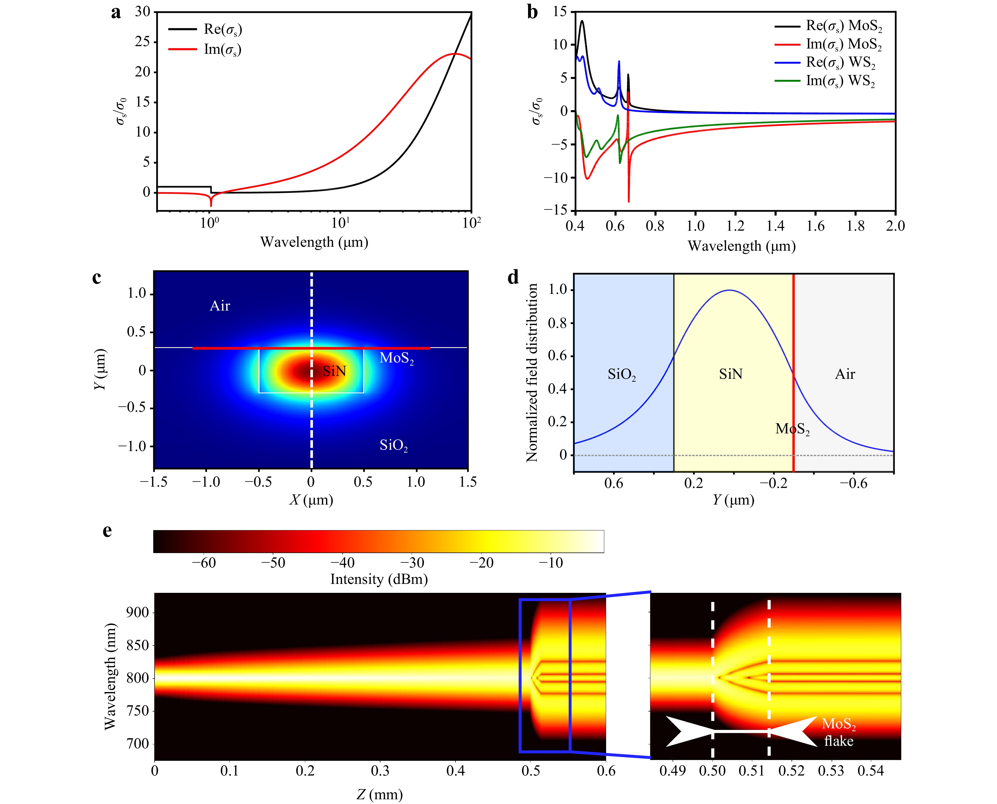
Fig. 2 Simulation examples of hybrid 2D material waveguides. a Linear surface conductivity of graphene calculated from Eq. 1 (Red curve for imaginary components black curve for real components). b Surface conductivity of two most common TMDs (i.e., MoS2, WS2) calculated from Eq. 354,58. c Typical Transverse electric (TE) mode distribution for a SiN planarized buried strip waveguide coated with MoS2 at 1550 nm optical wavelength. d Slice of the TE mode showing part of the mode overlapping the 2D material. The effective susceptibility tensor calculation of this structure takes into account the density of the mode with the nonlinearities of each part of the structure. e Evolution of the spectral envelope (in a logarithmic scale) along light propagation obtained from the simulation of pulse propagation in a SiN strip hybrid waveguide with a 14.8 μm long exfoliated WS2 flake transferred on top22. The waveguide has a cross-section of h = ~ 330 nm and w = ~ 760 nm. The WS2 sheet is directly transferred on top of the waveguide, thus triggering the evolution of the light pulse along propagation. The area where the WS2 flake is located is also zoomed in the right panel.
$$ {\varepsilon}_{r}=\frac{\varepsilon\left(\omega \right)}{{\varepsilon}_{0}}=1+{\sum }_{k=1}^{N}\frac{{f}_{k}}{{\omega }_{k}^{2}-{\omega }^{2}-i\omega {\gamma }_{k}} $$ (2) where $ {f}_{k} $ stands for the oscillator strength, $ {\mathrm{\omega }}_{\mathrm{k}} $ the resonance frequency, and $ {\mathrm{\gamma }}_{\mathrm{k}} $ is the spectral width of the kth oscillator. To access the surface conductivity, one can rely on a relation between surface conductivity and the material permittivity:
$$ \varepsilon\left(\omega \right)={\varepsilon}_{0}\left(1+\frac{i{\sigma }_{b}}{{\varepsilon}_{0}\omega }\right)={\varepsilon}_{0}\left(1+\frac{i{\sigma }_{s}}{{\varepsilon}_{0}\omega {h}_{eff}}\right) $$ (3) where heff is the effective atomic thickness of the thin layer 2D material, $ \varepsilon\left(\omega \right) $ is the permittivity, $ {\varepsilon}_{0} $ is the vacuum permittivity, $ {\sigma }_{b} $ is the bulk conductivity and $ {\sigma }_{s} $ is the surface conductivity. Fig. 2b displays the surface conductivity calculation for two of the most common TMDs (i.e., MoS2, WS2) using the data from Ref. 58. Retrieving the surface conductivity data is critical to model the opto-geometrical properties of the added 2D material. Typical calculated TE mode distribution can be seen in Fig. 2c, d and is not significantly different from the uncladded waveguide (see Refs. 59,60). As such, no additional coupling losses are to be expected. Although 2D materials have a very limited effect on the passive properties of the waveguides59,60, the additional phase shift from the 2D material is still required to be considered in several applications59,61.
Subsequently, as discussed in the next subsection, a precise knowledge of the interaction between the 2D material and the transverse propagating mode might be required in the case of nonlinear applications, notably because of the gigantic nonlinear properties of the added material. 2D materials are yet likely to introduce also additional propagation losses61, but as these losses are highly related to fabrication, transfer, and post-treatment methods (e.g., annealing), they are difficult to account for in numerical studies. In any case, worst case situations can be considered to assess the nonlinear performances of the devices embedding the 2D layers.
-
Nonlinear effects occur as a response to waveguiding structure materials during light propagation, including Four-Wave Mixing (FWM), Self-Phase Modulation (SPM), Second-Harmonic Generation (SHG), and Third-Harmonic Generation (THG). Mathematically, nonlinear optical phenomena can be expressed as an expansion of the polarization function of the medium where $ \mathbf{E} $ is the electric field and $ {\chi }^{\left(n\right)} $ is the nth order of the susceptibility tensor62:
$$ \mathit{P}\left(t\right) ={\chi }^{\left(1\right)}\mathbf{E}\left(t\right)+{\chi }^{\left(2\right)}{\mathbf{E}\left(t\right)}^{2}+{\chi }^{\left(3\right)}{\mathbf{E}\left(t\right)}^{3}+... $$ (4) Additionally, third-order nonlinearities induce phase modulation properties in the medium. This can be described by considering the phase-matching conditions63:
$$ \kappa ={\Delta \beta }_{L}+{\Delta \beta }_{NL}=0 $$ (5) where $ {\Delta \beta }_{L}=\sum _{k=0}^{\infty }({1}/{k!}){\left({\partial \beta }/{\partial \omega }\right)}^{k}{(\omega -{\omega }_{P})}^{k} $ and $ {\Delta \beta }_{NL}=2\gamma P $ , with $ P $ the peak pump power and $ \beta $ the optical mode propagation constant. $ {\Delta \beta }_{L} $ corresponds to the chromatic dispersion contribution to phase matching between the involved frequencies, a linear process derived from the opto-geometrical parameters of the waveguide. $ {\Delta \beta }_{NL} $ is the corresponding nonlinear component induced by the nonlinear response of the material and generating another phase shift. Here, the coefficient $ \gamma $ is the effective nonlinear coefficient accounting for the strength of the nonlinear response occurring during propagation in the waveguide. Basically, the nonlinear waveguide behavior scales as the real part of this coefficient and thus needs to be as large as possible. The linear phase mismatch $ {\Delta \beta }_{L} $ originates from the waveguide mode dispersion profile. The geometry of the structure and the composite materials set opto-geometrical parameters where properties and shapes must be studied in relation to each other. The Kerr nonlinear refractive index and the TPA coefficients of the waveguiding structure are generally introduced as n2 and βTPA respectively, and can be related as follows64:
$$ \frac{\omega }{c}{n}_{2}+\frac{i}{2}{\beta }_{TPA}=\frac{3\omega }{4{\epsilon }_{0}{c}^{2}{n}^{2}}\Gamma $$ (6) The effective nonlinear susceptibility tensor $ \Gamma $ directly expresses the contribution of every component of the hybrid structure. Every material is considered with its properties and weighted by the fraction of the mode overlapping with each part of the waveguide’s cross-section. Subsequently, $ \Gamma $ can be calculated as:
$$ \Gamma =\frac{{A}_{0}{\int }_{{A}_{NL}}^{}\overline{e}(r;\omega ){\chi }^{\left(3\right)}e(r;\omega )\overline{e}(r;\omega )e(r;\omega )dA}{{({\int }_{{A}_{\infty }}^{}{n}^{2}\left(r\right){\left|e(r;\omega )\right|}^{2}dA)}^{2}} $$ (7) with ANL the transverse area is occupied by nonlinear materials, $ {A}_{\infty } $the whole cross-section area, A0 the area of the waveguide’s core, $ e(r;\omega ) $the transverse electromagnetic mode distribution, and $ \overline{e}(r;\omega ) $its complex conjugate. This parameter is a complex number that can be separated into its real and imaginary parts: $ \Gamma =\Gamma \text{'}+j\Gamma \text{'}\mathrm{\text{'}} $64. $ \Gamma \text{'} $ accounts for the refractive index variations, whereas $ \Gamma \text{'}\text{'} $ accounts for the nonlinear TPA. This parameter does not provide a useful comparison between different waveguide structures. A more informative factor is the effective nonlinear coefficient $ \gamma $, mentioned in Eq. 5 which considers the mode group velocity vg:
$$ \gamma =\frac{3\omega \Gamma }{4{\epsilon }_{0}{A}_{0}{v}_{g}^{2}} $$ (8) This factor carries the information of the nonlinear Kerr coefficient expressed with the real part of $ \gamma $ and the TPA with the imaginary part. The numerical integral over the whole waveguide cross-section from Eq. 7 must include the properties of different nonlinear materials. The 2D material can then be considered as a bulk layer with a thickness of heff. This is critical to consider the overlap between the transverse mode and the huge nonlinearities of the material. This simulation methodology thus makes it possible to study different typical hybrid waveguide geometries, regardless of the location or the number of 2D sheets, and to derive both the dispersion properties of the hybrid waveguides and their effective nonlinearities.
A more intuitive and complementary measure of the situations to be investigated consists simply in evaluating the total fraction of the power passing through the active material, i.e., the confinement factor in the active material60. To do so, we derive the Poynting vector through the effective thickness of the layered material and the Poynting vector through the whole structure:
$$ \mathbf{S}=\mathbf{E}\times \mathbf{H} $$ (9) S is the Poynting vector, E is the electric field, and H is the magnetic field. To describe the propagating energy responsible for nonlinear effects occurring in the waveguide, the average power flow through the wanted area is derived from S:
$$ ⟨P⟩=\left\langle{\iint \mathbf{S}.{u}_{z}ds}\right\rangle $$ $$ CF=\frac{{\left\langle{P}\right\rangle}_{2D}}{{\left\langle{P}\right\rangle}_{tot}} $$ (10) where <> denotes a time average and CF the confinement factor. $ {\left\langle{P}\right\rangle}_{2D} $ is thus the power flow through the 2D material only and $ {\left\langle{P}\right\rangle}_{tot} $ the power flow through the cross-section of the waveguiding structure. Knowing how much the 2D material contributes to the effective nonlinearity allows the calculation of its nonlinear Kerr refractive index from the experimental characterization of the hybrid waveguide (e.g., SPM or FWM measurements)25. This means that this formalism can be used both ways, as a means of anticipating the effective performances of waveguide structures through simulation and optimization on the one hand60, and as a way to trace back the contribution of the 2D materials from experimental data22 on the other hand.
-
From the effective nonlinear optical properties of waveguides, it is possible to describe the propagation of optical pulses numerically. Third-order nonlinear effects, free carriers, and linear passive losses are the main effects to be included in the model to match experimental results as closely as possible. Commonly used for that purpose, the propagation of nonlinear pulses can be modelled using the generalized nonlinear Schrödinger equation (GNLSE)63–65:
$$ \begin{split}&\frac{\partial A}{\partial z}-\frac{\alpha }{2}A-\left(\sum _{k\ge 2}{\beta }_{n}\frac{{i}^{n-1}}{n!}\frac{{\partial }^{n}}{\partial {T}^{n}}\right)A-\left(\frac{{\sigma }_{a}}{2}+i{\sigma }_{n}\right){N}_{C}A\\=&i\gamma \left(1+\frac{1}{{\omega }_{0}}\frac{\partial }{\partial T}\right)\times \Bigg(\left(1-{f}_{R}\right)A{\left|A\right|}^{2}\\&+{f}_{R}A{\int }_{0}^{\infty }{h}_{R}\left(\tau \right){\left|A\left(z,T-\tau \right)\right|}^{2}d\tau \Bigg) \end{split}$$ (11) with A the complex envelope, α the attenuation constant, βn the higher-order coefficients from the Taylor expansion of the propagation constant calculated around the central frequency $ {\omega }_{0} $. Free carriers are described using the following parameters: $ {\sigma }_{a} $ and $ {\sigma }_{n} $ are the free carrier absorption and refraction coefficients, and $ {N}_{C} $ is the free carrier density64,66. The Raman response is considered with $ {f}_{R} $, the delayed Raman response to polarization63,67, and $ {h}_{R}\left(t\right) $ the Raman response function. TPA can be expressed in this equation as the complex part of the nonlinear coefficient $ \gamma $64. The different effects can be neglected or not, depending on the case. For instance, the Raman response is usually neglected for simulations in integrated optics for the Si or SiN platforms64,68. Free carriers and TPA can be further ignored when using materials that do not trigger such effects in the frame of wavelengths used during the experiments (e.g., doped silica waveguides or SiN waveguides around 1.5 µm). Regardless, the GNLSE can be used for fitting purposes22,32,34,68. Using the nonlinear coefficient γ as the fitting parameter, it is possible to retrieve the effective nonlinear performances of a waveguide. An extended literature review exists on numerical methods for integrating this equation, such as the split-step Fourier method using a fourth-order Runge-Kutta scheme for the integration63,67,68. Retrieving the effective nonlinear coefficient of a waveguide by fitting experimental spectra using Eq. 11 is an important link in the characterization of hybrid waveguides. When realizing pulse-broadening experiments in hybrid waveguides, it can be used to retrieve the effective nonlinear coefficient. Together with Eq. 7, this can be combined to retrieve the nonlinear refractive index of the 2D material itself. It must be pointed out that the longitudinal variation of the nonlinear coefficient needs to be addressed for more accurate results. Because current transfer methods rarely allow for full coverage of the device, it is frequently the case that optical pulses propagate in at least two different types of structures consecutively between light injection and collection in and out from the chip. Therefore, a longitudinal profile of the nonlinear coefficient along light propagation must be considered to perform realistic numerical modelling of experiments. This is illustrated here by Fig. 2e, where a flake of WS2 was deposited on a fraction of a waveguide. The reports of such approaches have shown promising results, with extracted Kerr index and TPA coefficient values for the 2D material comparable to those reported in the literature22. Note that all our abovementioned theoretical discussions (e.g., modeling linear and nonlinear optical properties, pulse propagation in hybrid waveguides) on silicon waveguide examples apply to cylindrical silica optical fiber waveguides and can be extended to new frequency generation processes beyond the highlighted pulse broadening effect.
-
The main components of a hybrid waveguide are the photonic chip itself and the 2D materials. The processes have been well studied and optimized for the fabrication of integrated waveguides in the lab. Starting with the manufacturing, one can distinguish three main methods to fabricate 2D materials: Mechanical Exfoliation (ME)69,70, Liquid Phase Exfoliation (LPE)71 and Chemical-Vapor-Deposition (CVD)72. All these cases have advantages and disadvantages. For example, mechanical exfoliation usually delivers the best crystal quality, the uncertainty of the process of low volume makes it difficult to scale up at industrial levels. Other methods, such as LPE or CVD, offer much bigger volumes and are promising for industrial scale, but the quality of the materials remains to be improved.
Fabrication of the 2D materials is one side of the process. After, 2D materials need to be transferred on top of the integrated photonic chip. The great majority of the existing work on hybrid waveguides utilize direct transfer methods, such as wet transfer73,74 (fishing of the 2D material in suspension in a solution), dry transfer75 (deposition of the material using a polymer stamp) or semi-dry transfer76. However, the field has recently seen a few publications attempting direct growth of 2D materials via CVD on the chip77,78. This method could prove itself revolutionary as it would circumvent most of the problems arising in more conventional methods (polymer residue, small scale of the deposit,…), which however needs further investigation for deterministic hybrid waveguide fabrications at a large scale.
-
The denomination “2D material” designates a thin crystal layer with a thickness of just a few atoms. No material is completely 2D and does have an effective thickness heff (usually a few nm). This corresponds to the atomic thickness of the material in the case of monolayer or few-layer crystals. The 2D material category includes graphene, a honeycomb structured layer of carbon atoms that was first demonstrated thanks to mechanical exfoliation70. Its unique electronic and optical properties79–81, sparked enormous interest in 2D materials, and prompted the discovery of numerous other thin-layer crystals with interesting physical properties82. Other 2D materials (such as TMDs, BP, or hexagonal Boron-Nitride (h-BN)) have also been widely studied. Fig. 1 presents typical “honeycomb-like” structures of 2D materials that differ in the nature of their band gaps and their group of symmetry (e.g., D6h for graphene, D3h for typical TMDs83). These variations can be exploited to get the best out of hybrid integration depending on the targeted optical functions (e.g., switch operation, broadband light sources84).
2D materials show very promising performance in terms of optical nonlinearities23,51,84, as illustrated in Table 1 with the characterized nonlinear response of various hybrid waveguides. Second-order nonlinear effects (like SHG)85,86 and other nonlinear effects (such as Raman emission and saturable absorption) can also be reinforced thanks to 2D materials. However, assessing the nonlinear optical properties can prove challenging. A lot of discrepancies can be found between different references and characterization methods. This can be attributed to the influence of the layer fabrication methods and the quality of the thin layered crystal and their properties23,51. For example, some fabrication and deposition methods leave more residues (e.g., polymer, water), defects in the monolayer crystal, and wrinkles of the flake87. For instance, a CVD-grown sample (e.g. CVD grown graphene prompting $ {\chi }^{\left(3\right)}=~5-10\times {10}^{-19}\;{\rm m}^{2}{\rm V}^{-2} $ from THG measurements with a pump at 1566 nm88) presents different performance than an exfoliated one (e.g., $ {\chi }^{\left(3\right)}=~4.2\times {10}^{-15}\;{\rm m}^{2}{\rm V}^{-2} $ for exfoliated graphene measured from THG measurements with a pump at 1550 nm89). Doping can also generate variation in the measured nonlinear response90–92. Moreover, the environment surrounding the 2D materials (e.g., the substrate93), and induced strain94–97 also affect results. The characterization method itself is an important aspect of this matter. An in-plane electromagnetic wave excitation produces different results than an out-of-plane one23,98–100. In connection with this question of the optical excitation mode of 2D sheets, it was shown that for graphene and GO a quasi-TE polarization in the waveguide triggered higher responses than the quasi-TM polarization99-101. Some preliminary studies suggested this might also be true for TMDs, such as MoS292.
The study and deep understanding of the nonlinear properties of 2D materials remain challenging. Most previous studies are based on experimental measurements without any strong link with the theoretical origin of the observed properties. In this view, the exception is again graphene, its Dirac-cone shape band structure allowing for analytical investigation of the third-order conductivity, i.Fe., equivalent to the third-order susceptibility in a bulk material as for its linear properties. Thus, the analytical solution for $ {\sigma }^{\left(3\right)} $, a surface equivalent of the susceptibility tensor $ {\chi }^{\left(3\right)} $, can be explicitly expressed98. For other 2D materials, understanding the mechanisms requires iterative comparisons between experimental results and numerical modelling and analysis, raising at the same time a difficulty but also opening a very interesting field of investigation to explore to evaluate their full potential. Undoubtedly the theoretical understanding of the optical properties of 2D materials will continue to grow in the coming years, as well as the hybrid integration with waveguides simultaneously. However, for the time being, progress and research must mainly rely on experimental results, particularly in the case of newly discovered materials.
-
Integrating 2D materials on photonic chips is beneficial in various ways102. We have witnessed that hybrid integration of 2D materials not only enhances the nonlinear optical performance of waveguides, but also introduces new nonlinear optical properties that are impossible with the waveguide before the integration. This section focuses on second and third-order parametric and a few nonparametric optical processes62.
-
Finding reliable materials to boost the effective third-order nonlinear response of a waveguide while remaining TPA-free is critical for silicon-based waveguides. Whereas some 2D materials present photon absorption around 1.5 µm wavelength (such as graphene, due to its gap-less nature103), other families of 2D materials, such as TMDs, have a gap large enough to limit photon absorption in the wavelength range of interest102–104. Related to this, experimental data collected from integrated optics and free space measurements are summarized in Table 1. Although results can vary significantly from one characterization method to another, performances are generally promising with high reported Kerr refractive indices compared to standard materials of the CMOS platform (see $ {n}_{2} $ comparison for different materials in Table 1). Here we summarize the hybrid integration results of using third-order optical nonlinearities.
-
SPM may be one of the easiest methods to measure third-order nonlinearities in a waveguide. Indeed, this phenomenon relies on the Kerr refractive index-induced phase shift during light propagation throughout a waveguide. Thus, this occurs in a typical regime of the waveguide’s chromatic dispersion for the guided mode and can be measured by pulse broadening. Fig. 3 presents several cases of different 2D materials. By adding a highly nonlinear material to the waveguide, a higher effective nonlinear refractive index (n2) is expected, thus causing a more substantial broadening of the output spectrum after a given constant propagation distance (Fig.1). Therefore, measurements of the output spectra can convey information regarding the effective properties of the hybrid integrated waveguide structure. Usually, simulation data calculated by integrating the GNLSE are matched with measurements. For all cases presented in Fig. 3, a more significant broadening effect is obtained from the waveguide with a 2D material on top due to the enhanced SPM of the 2D materials26,63,107.
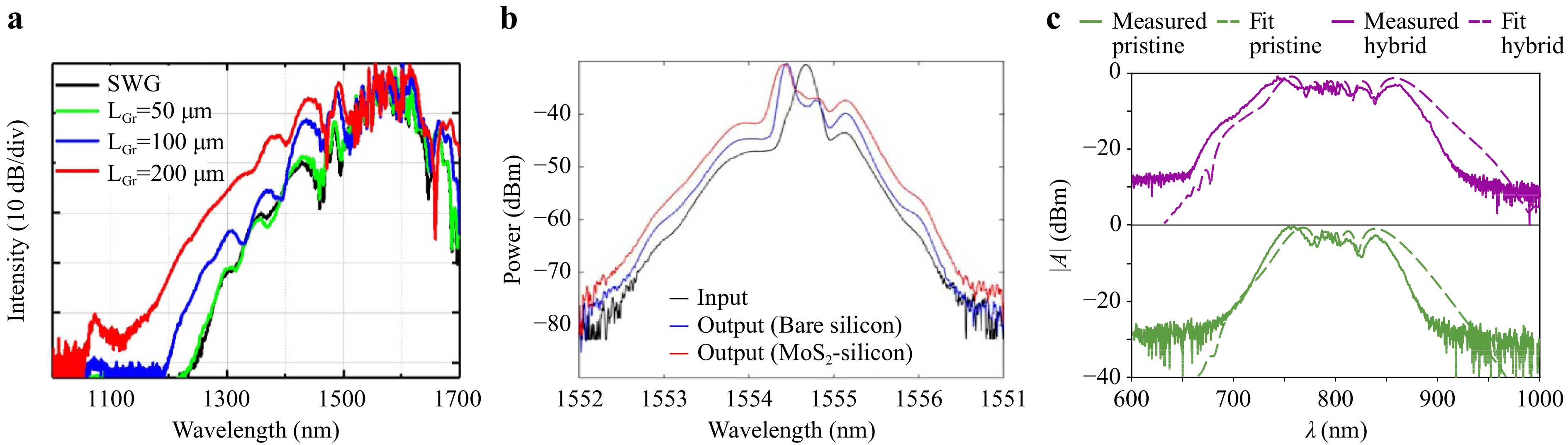
Fig. 3 SPM enhancement results with 2D materials covered waveguides. a SPM measurements in graphene-covered silicon waveguides. Measurements were done for several lengths (LGr) of graphene sheet-covered waveguides in contrast with a pure silicon waveguide (SWG) using a pulsed pump at 1560 nm wavelength with a 250 MHz repetition rate, 80 fs pulse duration, and an input pulse energy of 120 pJ 32. b SPM measurements in a planarized buried strip silicon on insulator (SOI) waveguide enhanced with MoS2. The pump is a pulsed laser with a 1 MHz repetition rate and a pulse width of 56 ps at 1554.5 nm26. c SPM measurements in a SiN waveguide integrated with WS2. The pump is a pulsed laser-centered around 800 nm with an 85 MHz repetition rate and a TE-duration pulse of 100 fs22.
Results highlighted in Fig.3 show significant broadening spectra for the hybrid waveguides compared to the reference (bare waveguides). Fig. 3a presents larger spectral broadening effects for different lengths of graphene. The full potential of various 2D materials in a guided configuration for Kerr effect enhancement of waveguides was thus successfully demonstrated and quantified using methods discussed in Section 2. An effective nonlinear refractive index of ~ 4.1 × 10⁻¹⁷ m2/W was retrieved for graphene32 (Fig. 3a). Other similar work in graphene also confirms ~ 2 × 10⁻¹⁷ m2/W34. SPM also has been demonstrated with planarized buried strip SOI waveguides integrated with MoS2 (Fig. 3b), giving an effective nonlinear refractive index for MoS2 of ~ 1.1 × 10⁻¹⁶ m2/W26. Ref. 22 reported a n2 of ~ 2.18 × 10⁻¹⁵ m2/W for WS2 (Fig. 3c). Note that those reported n2 values are consistent with the results measured with other characterization methods such as FWM (see Table 1). To offer more complex optical functions (e.g., broadband, and ultrashort light sources), future developments are expected, such as using longer spiral waveguides, integrating 2D materials inside the waveguides, using heterostructures or alternative layers60 with enhanced nonlinearities. Beyond the spectral applications to the Kerr effect, Kerr modulation can also be introduced and enhanced using 2D materials, as in the example of a fiber-based all-optical Kerr phase shift modulator108. Undoubtedly, similar usage of 2D materials will be developed for the fiber integrated platform as well.
-
FWM is one of the most widely used third-order nonlinear optical functions for applications, such as all-optical parametric amplifiers and photon pairs109,110. FWM is often found in its degenerate form, where $ 2{\omega }_{P}={\omega }_{s}+{\omega }_{c} $, according to the conservation of energy and $ 2{k}_{P}={k}_{s}+{k}_{c} $ according to the conservation of momentum. Here, degenerate FWM involves 3 frequencies ($ {\omega }_{p} $, $ {\omega }_{s} $ and $ {\omega }_{c} $) and their wavenumbers ($ {k}_{P} $, $ {k}_{s} $, and $ {k}_{c} $) for the pump, the signal, and the converted frequency (idler), respectively. FWM is most effective when the frequencies are phase-matched together. In the absence of TPA, the efficiency of the FWM process can be characterized in terms of conversion efficiency111–114:
$$ {\eta }_{straight}=\frac{{P}_{C}\left(L\right)}{{P}_{S}\left(0\right)}={\left|\gamma {P}_{0}{L}_{eff}\right|}^{2}\mathrm{e}\mathrm{x}\mathrm{p}(-\alpha L) $$ (12) with $ {P}_{C}\left(L\right) $ the power of the converted frequency after propagation in a waveguide of L length, $ {P}_{S}\left(0\right) $ the input signal frequency power, $ {P}_{0} $ the input pump power, α the propagation loss, and the effective propagation length Leff:
$$ {L}_{eff}=\frac{1-{e}^{-(\alpha +j\kappa )L}}{\alpha +j\kappa } $$ (13) where κ is the phase mismatch. FWM conversion efficiency can be further enhanced if we use a resonator. However, the integration of 2D materials with a microresonator (e.g., a micro ring resonator) must be carefully considered because of the influence of the thin layer material on the cavity’s passive properties59,115,116. The new equation for the conversion efficiency becomes112,113,117–119:
$$ {\eta }_{resonator}=\frac{{P}_{C}\left(L\right)}{{P}_{S}\left(0\right)}={\left|\gamma {P}_{0}{L}_{eff}\right|}^{2}{FE}_{p}^{4}{FE}_{c}^{2}{FE}_{s}^{2}\mathrm{e}\mathrm{x}\mathrm{p}(-\alpha L) $$ (14) where FEi is the field enhancement factor and can be expressed as follows in an all-pass ring:
$$ {FE}_{i}=\left|\frac{k}{1-r{e}^{\frac{-\alpha L}{2}+j\frac{{\omega }_{i}L}{c}}}\right| $$ (15) The field enhancement factor is responsible for improving the FWM performances in a ring compared to a straight waveguide. Reciprocally, FWM frequency conversion can also be used as a useful means of characterization of hybrid optical waveguides. By measuring the gain on the converted frequency, one can retrieve the waveguide’s effective nonlinearities. This method was used in numerous examples for different materials due to its reliability and relatively easy implementation. Fig. 4 shows examples of FWM studies carried out for various hybrid waveguides embedding 2D materials. Those studies were either performed in micro-ring resonators (Fig. 4a−f) or regular waveguides25
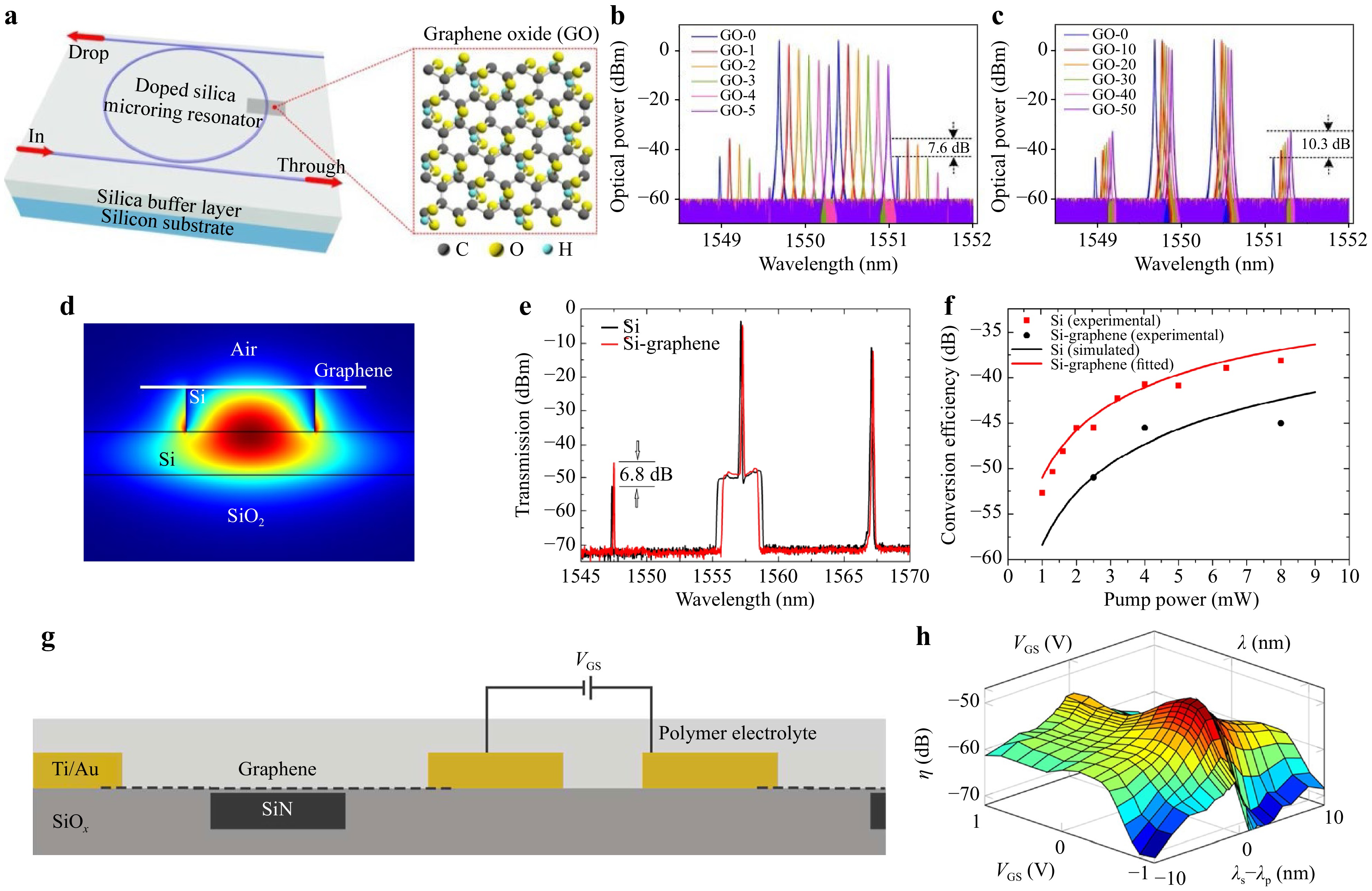
Fig. 4 FWM results of hybrid integration with 2D materials. a−c FWM experiment conducted on GO coated Si-ring resonators 120. a Doped silica/silica micro-ring resonator coated with 1-50 layers of GO. In the zoomed-in inset: chemical representation of GO and its crystalline configuration. b FWM spectrum for 0-5 layers coating of GO. c FWM spectrum for 0-50 layers coating of GO. d−f FWM measurements in a graphene-coated Si ring-resonator31. d Cross section of a Si-ridge ring resonator. e Comparison between the FWM spectrum in a Si waveguide (black) and a Si-graphene waveguide (red). f Enhancement in the idler gain shows the conversion efficiency versus the pump power for both waveguides. g-h Gated graphene-SiN waveguide for tunable FWM, 122. g Gated planarized buried strip with graphene. h Results of conversion efficiency (FWM) versus the gate voltage (VGS) and the wavelength detuning between the pump and the signal.
Using the same reasoning as for SPM, it is then possible, knowing the overlap between the 2D material and the transverse propagating mode, to calculate the effective Kerr refractive index of the 2D material alone. A first example of the FWM approach to the use of hybrid waveguides is highlighted with a ring resonator coated with GO (see Fig. 4a)120. The Kerr refractive index of GO was extracted as ~ 1.5 × 10⁻¹⁴ m2/W. The injected pump was a 160-mW continuous wave source centered at ~ 1550 nm wavelength. As shown in Fig. 4b, c), the experiment was attempted for several thicknesses of the GO covering layer. The thicker the layer, the higher the nonlinear effect seems to be due to a higher interaction between the mode and the GO. For graphene (Fig. 4d−f), the nonlinear refractive index has been measured at ~1.5 × 10⁻¹⁷ m2/W31 with a pump and the signal set at resonances of the ring (1557 nm and 1567 nm, respectively). The gain on the idler is ~6.8 dB for a continuous power of 8 mW for the pump and 1 mW for the signal (Fig. 4e). The study also reports a typical behavior of the conversion efficiency versus the pump power (Fig. 4f), confirming the nonlinear origins of this increased performance in the hybrid waveguide. Similar experiments with MoS2 on a straight Si waveguide have also been reported (Ref. 25) with a Kerr refractive index of ~ 2.7 × 10⁻¹⁶ m2/W25. FWM was measured by injecting a 0.1 mW pump at ~ 1550 nm with a signal at ~ 1550.4 nm. The results between the reference waveguide and the MoS2-Si waveguide are compared to assess the effect of MoS2 on the waveguide’s properties. FWM results presented here are promising. Depending on the structure and nonlinear 2D material, a gain of up to 10.3 dB (Fig. 4c) on the idler frequency, the lowest being 4 dB for a straight waveguide in SOI (Ref. 25). This also shows the advantages of combining interesting integrated photonics structures with 2D materials. Additionally, 2D materials, such as graphene, can be combined with electrodes, introducing the tunability of the FWM. Indeed, inducing a biased current allows tuning the 2D sheet surface conductivity as a tuning of the Fermi level121. Fig. 4g, h presents an example of tunable effective nonlinear coefficient γ using gated graphene (with polymer electrolyte) combined with electrodes (see Fig. 4g)122. The applied bias voltage effectively induces a shift in the Fermi level, which translates into effective tunable properties of the waveguide (Fig. 4h). This can, of course, be expanded to wider and very promising nonlinear optical functions as the FWM process is involved in the generation of multiple nonlinear integrated functions (e.g., supercontinuum sources, frequency combs). Using the approaches illustrated in Fig. 4g, h, one can improve and diversify the possibilities of hybrid integration by introducing the device’s tunability. This is one more step toward fully integrated on-chip applications and other applications such as miniaturized spectroscopy123.
-
Frequency combs are broadband light sources of multiple equally spaced narrow frequency lines124. They can be formed under specific phase and pump power conditions inside a ring resonator3. To meet these phase-matching requirements, the ring waveguide GVD is required to be in the anomalous regime, thus requiring waveguide engineering63. The wider the anomalous window, the broader the frequency comb tends to be125. This phenomenon was established in the literature and can be understood thanks to the so-called Cherenkov radiations2,125. Kerr frequency comb generation is typically strongly relying on cascaded FWM. Hence, good performance in FWM is key to the development of efficient generation processes of frequency combs. Due to the recent advances in boosting FWM using hybrid integration schemes, the demonstration of frequency combs using hybrid devices with 2D materials is likely to be widely addressed in the next few years. Moreover, a report of tunable frequency combs enhanced with graphene has been reported. Using the Fermi-Dirac tunability of a gated graphene sheet on top of a micro-ring, the tunability of the GVD profile brought a tunability of the comb itself126 as well as a reported slight enhancement of the nonlinearity introduced by the graphene. In this work, a tunable laser (between 1480 nm and 1640 nm) was driven to mode-lock Kerr dissipative soliton pulse inside the cavity together with the control of the cavity chromatic dispersion thanks to the gated sheet of graphene. A bias current was applied to the graphene sheet covering the cavity’s waveguide. The proper flow of electrons was further guaranteed at the surface of the monolayer sheet using an ion gel. With different bias voltages applied, various Fermi levels for the graphene sheet can be electrically shifted, thus resulting in various frequency combs due to the shifting dispersion profile. Graphene is not the only material that could benefit this range of applications. Other 2D materials recently showed a lot of potential regarding the tunability of the micro ring cavity using gated TMDs61. The variations of the resonance induced by different biased currents can be explained by an effective index change of the propagative waveguide mode induced by the modified conductivity of the 2D material. From the tunability of the effective refractive index in Ref. 126, it was inferred that such tunable frequency combs could also be achieved in the future using other families of materials (such as WS262 or WSe2127). Beyond the benefit of the dispersion tunability, materials such as graphene can also weight on the gain-loss balance and thus further expand tunability. The optoelectronic feedback stabilization128 and chemical sensitization121 are also huge benefits of that approach for soliton combs. Supercontinuum generation can benefit from similar designs. Although, the complexity brought by cavities and mode-locking is removed as regular waveguides are generally used for that purpose, GVD engineering and optimization of the effective nonlinear properties are still required65.
-
Second-order nonlinear phenomena involve $ {\chi }^{\left(2\right)} $and are subject to crystal symmetry62. In a centrosymmetric medium, material polarization P is an odd function (P(-E) = −P(E)) E being the electrical field. Thus, to satisfy Eq. (4), $ {\chi }^{\left(2\right)} $ vanishes to 0. Hence, typical materials compatible with CMOS processes, such as Si or SiN do not present second-order nonlinear effects due to their centrosymmetric structures. Yet, second-order nonlinearities could be beneficial for ultrafast modulation of optical signals, which is required for signal processing. The free-carrier dispersion of p-n and p-i-n junctions typically used in the SOI technology for modulation is too slow130-132. Therefore, the ultrafast Pockels effect would be preferable, although it is challenging to engineer due to the nature of available materials. The introduction of such an effect relying on the hybrid integration of III/V semiconductors on Si was proven efficient for that purpose131. 2D materials could also be a promising solution to that end. However, materials presenting centrosymmetric crystal layouts (such as graphene, BP, or even numbers of TMD layers) do not provide second-order nonlinearity75,133. However, some methods exist to introduce SHG to centrosymmetric 2D materials. For example, introducing external electrical fields (in graphene134,135 or TMDs135-137) or doping the material91,138 showed promising results in that regard. On the other hand, other 2D materials (e.g., 3R phase BN and TMDs) can present second-order nonlinearity due to their non-centrosymmetric nature. As a pilot demonstration scheme of $ {\chi }^{\left(2\right)} $, SHG was particularly mainly studied. As such, promising SHG performance in terms of conversion efficiency was reported in free space27,29,51,86,139–141, but also in a few cases in integrated optics, as discussed in this section. SHG phenomena were investigated in various waveguide structures (see Fig. 5) regarding the intensity of the generated frequency (i.e., second harmonic: SH). For structures coated with a 2D material sheet, the evanescent field of the exciting wave (also referenced as a fundamental wave: FW) overlaps with the 2D material and could thus take advantage of the sheet's second-order nonlinearity. The SH frequency wave could then propagate in the integrated structures and be collected at the output. Similarly, to what has been established with other frequency conversion mechanisms (see the section relating to FWM), SHG can benefit from the boosting of a cavity57,142 (e.g., photonic crystal cavity142). It can be treated mathematically similarly to FWM (see Ref. 112 for SHG and Ref. 112,118 for FWM). The cases discussed here show larger enhancement with the hybrid cavity than in a more classic propagation scheme. In the reported experiments, samples were pumped with a 1550 nm wavelength laser for a generated signal at around λ = 630 nm. Thus far, the 2D materials considered in these experiments typically are WSe2, MoSe2, and WS2 for Refs.142,143, and 144 respectively. In the case of Ref. 142, the addition of the 2D materials induces a twofold increase in the conversion efficiency, reaching an impressive ~ 10−2 conversion efficiency. The dependence of the results on the pump power is a characteristic of a nonlinear phenomenon, proving the nonlinear origins of the results, thus confirming SHG. Accounting for the cavity, boosting this enhancement, the improvement was up to 200 times more than bare Si. Fig. 5a−c reports a 5-fold efficiency enhancement after waveguide integration. This example showed that in-plane, longitudinal and extended interaction between the FW frequency and the 2D material was beneficial in terms of conversion efficiency in the MoSe2/Si waveguide compared to MoSe2 layers deposited on a homogeneous Si substrate. This demonstrated that an integrated edge-based scheme provided a reinforced light-matter interaction compared to free space settings, as shown in Fig. 5b, with a prominent SHG peak compared to the free space measurements. Moreover, the nonlinear nature of this intensity increase was indeed demonstrated (Fig. 5c). Other works in optical fibers using various 2D materials coatings were also reported. The example in Fig. 5d, e is a micro-fiber coated with WS2 in which a factor of ~ 20 on the second harmonic intensity was reached143. As in previous examples, the nonlinear origin of this SHG intensity increase was confirmed by ramping the pump power (Fig. 5e). Additionally, work in hybrid photonic crystal fibers (PCF) has also been recently reported. In Ref. 144, PCFs coated with MoS2 and measured conversion efficiency of 10−4 to 10−3, an enhancement of 3 orders of magnitudes compared to planar 2D MoS2. Additionally, other results with various 2D materials combined with different integrated structures have also shown great results (e.g., monolayer GaSe on a photonic crystal (PhC) cavity145, GaSe146 or InSe147 on microfibers). All these results and trends collected on the enhancement of second-order nonlinear effect by the integration of 2D materials on waveguide photonic structures have opened promising application opportunities as a reliable approach to induce effective second-order nonlinearities in Si- photonics that is difficult to induce by other approaches and by relying on classical Si compatible materials (e.g., Si, SiO2, SiN). Enabling SHG for these platforms will extend the range of applications and possibilities. For example, the realization of on-chip optical parametric oscillators, as presented in Ref. 148 (in aluminum nitride) or the generation of entangled photons sources with the pair photon generation enabled by SHG for quantum applications (as depicted in Ref. 149 in lithium-niobate) could become a reality for CMOS compatible platforms, using 2D materials as the second order nonlinear medium.
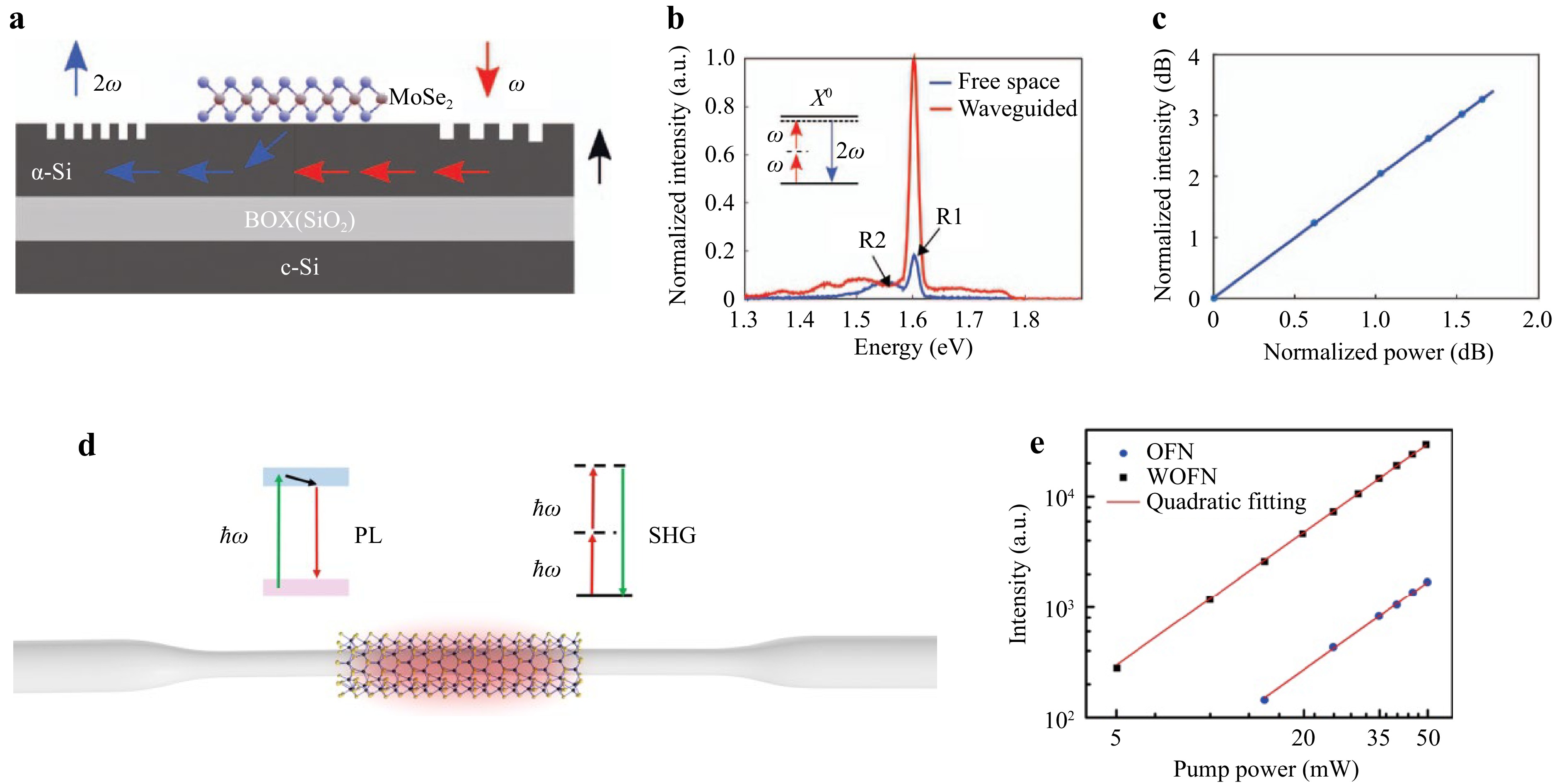
Fig. 5 Examples of SHG enhancement in various hybrid structures. a−c SHG enhancement with a MoSe2 integrated planar Si waveguide143. d Schematics of the device. A grating coupler is designed for the pump at the input and the generated frequency at the output. e Measured spectrum with a significant increase in the SHG emission for the hybrid structure. Peak R1 corresponds to SHG, and peak R2 to PL. f SHG intensity versus the input power. d and e SHG enhancement in a WS2 covered optical fiber144. d Optical fiber coated with the 2D material and occurring phenomena during propagation. e SHG intensity versus the input power. The WS2-optical-fiber-nanowire (WOFN) is here compared to the pure optical-fiber-nanowire (OFN).
-
Raman scattering originates from the coupling between the incident light and the vibrational frequency of the medium (atoms or molecules)62. Materials thus show different responses due to their different eigen-vibrational states. In fact, this is largely used to identify 2D materials based on their Raman signatures150,151. Although this effect is widely studied and exploited in free space, very few examples of Raman applications in the 2D material hybrid platforms exist. For example, some studies have shown a reinforcement in the Raman response of graphene by integrating it on top of a 2D slab of a PhC cavity152,153. Fig 6 shows two examples of enhanced Raman response in graphene using this integration method. PhC cavities were designed here using a three-hole defect (L3) cavity (Fig. 6a, d)154, which allowed for direct normal coupling inside the cavity. This cavity was designed for the cavity modes to correspond to the proper excitation wavelength of graphene for an optimal Raman response at 532 nm. The Raman mapping of the cavity (intensity of peak G and 2D as depicted by Fig. 6b) shows a large increase in the cavity (Fig. 6c). In a similar fashion, different measurements performed at key locations (locations are represented in Fig. 6d) show a large increase in PL and Raman signature for measurements performed on the cavity (red curves for Fig. 6e). As depicted in both examples presented in Fig 6, the combination of a cavity and a 2D material strengthens the Raman response of the 2D materials. Fig. 6c, e shows a significant increase with a 3.5 and a 6.1-fold enhancement in the Raman emission, respectively. Moreover, using these L3 PhC cavities allows normal, direct injection into the cavity, making the characterization process easy. As pointed out in Ref. 152, other types of photoemissions (PL for instance) from other 2D materials could also be enhanced using this principle155. This is a promising step for characterization purposes.This enhanced interaction between 2D materials, and the probing light might resolve limitations in the current characterization methods by improving the magnitude of the obtained signal. Other 2D materials, such as TMDs or h-BN, will also provide interesting alternatives to graphene for this kind of application, thanks to the nature of their bandgap offering other possibilities. Photoluminescence in 2D semiconductors (e.g., TMD), or harmonic generation (SHG, THG, higher harmonic generation (HHG)) might also be investigated using PhC devices. Furthermore, Raman effect could be leveraged in the generation of broadband light sources (as demonstrated in Ref. 156), thus expanding the range of possibilities in achieving efficient on-chip nonlinear optical functions.
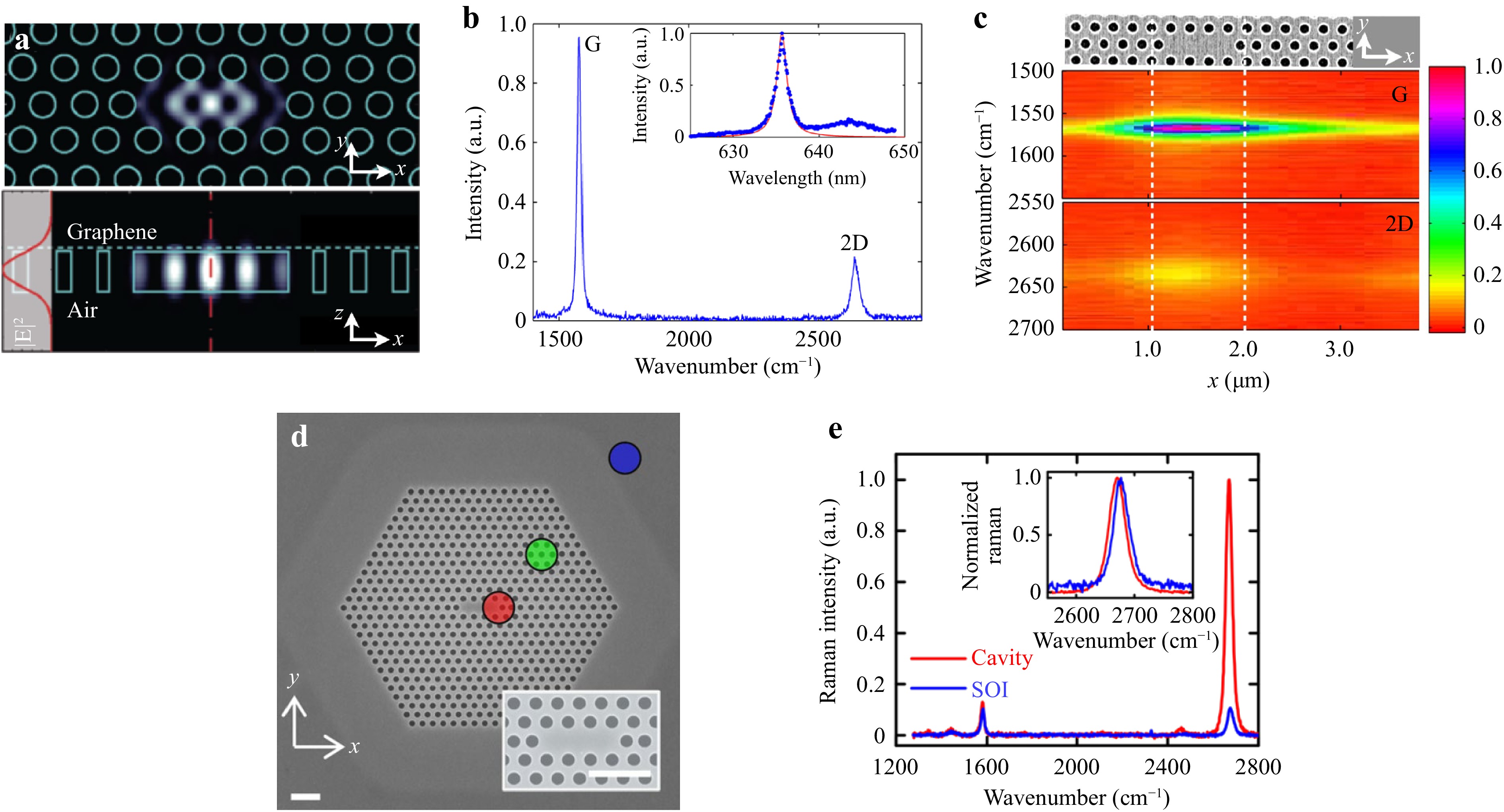
Fig. 6 Raman response enhancement using graphene-integrated PhC cavities. a−c Enhancement of the Raman response in graphene deposited on a Si-L3 cavity153. a In-plane (top) and cross-section (bottom) energy distribution of the fundamental mode of the PhC L3 cavity (simulation). b Raman response for excitation at 637 nm wavelength. The resulting spectrum shows two characteristic peaks (G at 1578 cm−1 and 2D at 2640 cm−1). The cavity resonance, set at 636 nm, is displayed in the inset. c Normalized emission intensity for the two peaks G and 2D, showing the spatial distribution. The Scanning electron microscopy (SEM) top image shows the corresponding localization. d−e Enhancement of the Raman response on graphene deposited on a Si-L3 cavity152. d SEM image of the PhC L3 cavity. Scale bars are 1 µm. The inset is a zoomed-in image of the cavity. e Raman spectrum of graphene for excitation at 532 nm. The spectrum is taken at two locations on the device: red for the cavity and blue for the SOI plane substrate. In the inset: zoomed-in on the normalized 2D peak for spectral comparison.
-
Until now, we considered absorption to be avoided due to its attenuation nature. However, absorption can also be an ally for applications due to its nonlinear properties. For several applications, TPA, a nonlinear conducting/semiconductor materials media property, can be exploited to trigger new effects. For example, because of the absorption of propagating photons through nonlinear processes such as TPA, free carriers are generated157 and affect the propagating waves. In a bulk medium, this can be accounted for by calculating the dynamic of the free carrier’s population using the imaginary part of the effective susceptibility tensor $ \Gamma \text{'}\text{'} $64.
$$ \frac{\partial N}{\partial t}=-\frac{N}{{t}_{c}}+\frac{3{\beta }_{1}^{2}{P}_{0}^{2}\mathrm{\Gamma }\text{'}\text{'}}{4{\epsilon }_{0}\hslash {A}_{0}^{2}}{\left|u\right|}^{4} $$ (16) with u the normalized field amplitude and tc the carrier lifetime.
In the context of a 2D sheet of graphene, it was established that due to Pauli blocking, inter-band transitions from the valence band to the conduction band become less likely as the electronic states of the conduction band are filled158. Hence the absorption becomes less probable, effectively translating into a saturation of the absorption process. In this context, it is thus more accurate to use an alternative expression describing the carrier population dynamic accounting for this saturation effect159:
$$ \frac{\partial N}{\partial t}=-\frac{N}{{t}_{c}}+\frac{{\alpha }_{sat}}{\hslash \omega }\left(1-\frac{N}{{N}_{sat}}\right)\frac{{\left|u\right|}^{2}}{w} $$ (17) The overall absorption in the 2D material-covered waveguide can then be written as such:
$$ \alpha \left(N\right)={\alpha }_{NS}+{\alpha }_{sat}\left(1-\frac{N}{{N}_{sat}}\right) $$ (18) where $ {\alpha }_{NS} $ is the non-saturable component of the absorption, Nsat is the saturated carrier density, and w accounts for the interaction length between graphene and the propagating mode within the transverse cross-section and corresponds to the waveguide width. Here, we present several examples of devices based on the saturable absorption properties of graphene (Fig. 7). Adding graphene on top of SiN/SiO2 (Fig. 7a, b) or SOI (Fig. 7c, d) waveguides (strip or slot waveguides as depicted in Ref. 161) allows for the introduction of saturable absorption to the silicon platform. The graphene sheet modifies the effective properties of the waveguide by interacting with the propagating mode overlapping with the 2D layer, as shown in Fig. 7a. Accordingly, transmission measurements show a saturation of the absorption as the injected power is increased (see Fig. 7b, d) even more if the interaction length between graphene and the mode is increased (see Fig. 7b, d). Adding saturable absorption properties allows for the design of new optical functions such as mode-locking, modulation160,161, and optical switching162. Whereas graphene has been the most studied, other materials are also available, operating at various wavelengths. For instance, MoS2 shows promising results both at 1 and 1.5 μm162,163. More generally, many different materials have been investigated for their saturable absorption properties, characterized in different guided settings (PCF, tapered fibers, or microfibers), showing the promises in terms of integrated optics (because of the similarity in the propagating evanescent field interacting with the material of interest)159,164,165. The variety of materials and fabrication/integration methods also allow for expanding the spectral range. In a 1 μm regime, work in a PCF was reported with a coating of the topological insulator Bi2Te3166. Other materials operating at this wavelength could also be investigated as they have shown promising results in unguided settings (graphene167, WS2168, MoS2169, BP170, etc.). Similarly, for the 1.5 μm regime, several results in guided settings have been reported using different 2D materials such as Bi2Se3 in PCF171, Bi2Te3 on a microfiber172, Heterostructures may also be investigated, MoS2/graphene, WSe2/MoS2, h-BN/graphene and other nanocomposite films have shown interesting results173-176. The extensive work conducted on saturable absorption has enabled the development of various functions such as Q-switching of mode-locking for short pulse duration laser with excellent performances down to the femtosecond regime176,177.
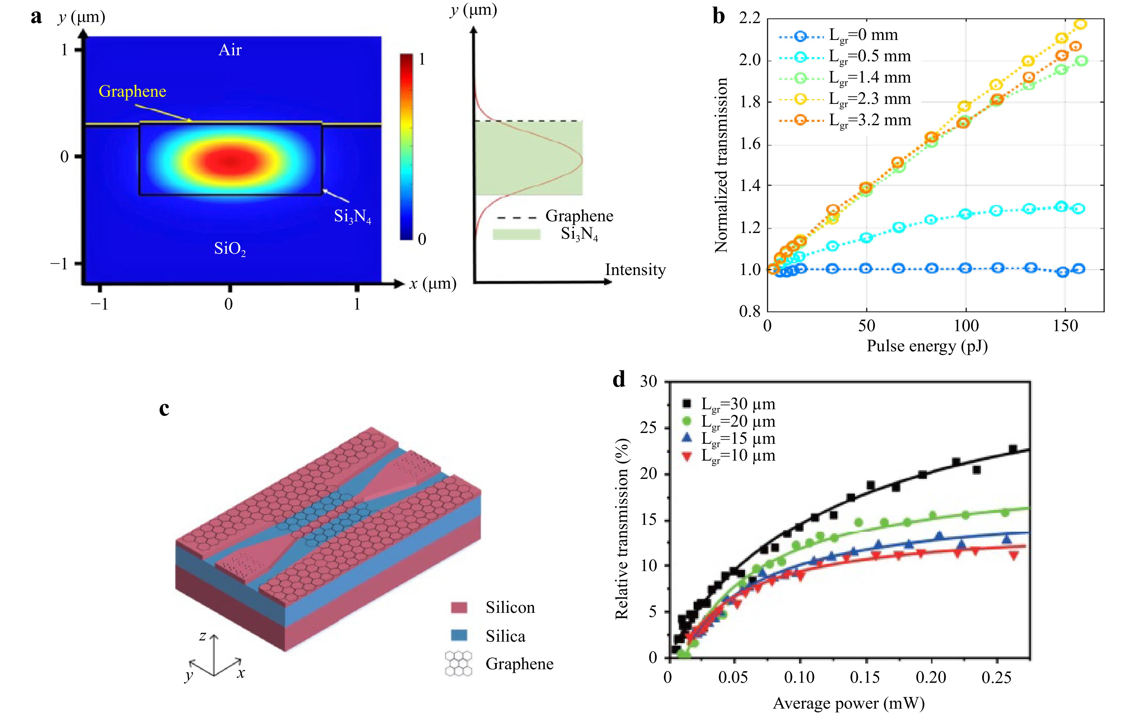
Fig. 7 Examples of graphene saturable absorption in CMOS-compatible waveguide structures. a and b Saturable absorption in a graphene-covered SiN waveguide159. a Transverse mode distribution of a graphene-covered planarized SiN buried strip. On the right, a slice of the cross section shows the density of the mode around the graphene layer. b Transmission in this waveguide measured for several lengths of graphene covered waveguides. c and d Saturable absorption in a graphene-SOI strip waveguide160. c Strip graphene-Si waveguide. d transmission measurements for different graphene lengths on top of the waveguides.
-
The current successful demonstrations have shown that the physical limits of different integrated optics platforms could be bypassed with their integration with 2D materials. The demonstrated properties indeed offer versatility and have demonstrated their improved performances in the context of hybrid structures. Further, 2D materials also introduce new functions (e.g., physical, chemical, and biological tuning). Nevertheless, a lot of gaps still exist in the available state of the art regarding the integration of 2D materials with waveguide structures. Performances can widely vary depending on the integration process and the environmental disturbances. Yet, many developments and breakthroughs can be expected from the relevant fields in the upcoming years. New Van der Waals crystals heterostructures are being investigated and are showing interesting results for their physical properties141,178. Additionally, the focus has been mainly put on graphene and TMDs, but other materials should also be considered (e.g., Kerr effect in GaS-SiN waveguides49, or SHG in NbOl2140). It is expected that new original types of integrated photonics structures will also emerge for various applications (e.g., spectroscopy179, all-optical computing180). Beyond the progress achievable in the design and fabrication of hybrid structures, it is likely that many different applications could benefit from this approach.
-
Putting an emphasis on maximizing the interaction between the 2D materials and the propagating light can be beneficial for characterization purposes. Indeed, it has been stated that these newly discovered materials (with only a couple of decades of research behind it) need more studies to increase the understanding of the community regarding their physics, especially their nonlinear properties. The enhanced measured nonlinear response emerging from increased interaction between light and these exceptional atomic-layered materials highlighting gigantic nonlinear susceptibilities, might both provide a powerful route to unveil new knowledge about this class of materials and to open avenues for a broad set of applications relying on their integration within classical photonic platforms. The use of integrated cavities, such as ring resonators or PhC cavities (with low-volume optical modes and high-quality factors), has already demonstrated interesting outcomes153. It is bound to yield more data and information as research continues. Coupled with this experimental aspect, such optimized devices are likely to find a use for designing efficient integrated functions.
-
The majority of nonlinear optical research on 2D materials uses graphene, TMDs, hexagonal BN, and BP. There are thousands of 2D materials, which might provide new materials with high nonlinearity (e.g., the recently reported 1D van der Waals semiconductor fibrous red phosphorus181, NbOl2140). Further, heterostructures (including mixed-dimensional heterostructures182,183 and Moiré heterostructures) have been reported for saturable absorbers184, which will be significantly extended to different integrated nonlinear optics (e.g., SHG185, THG186,187, and HHG157).
-
Thus far, most of the demonstrated hybrid 2D material-waveguide devices were fabricated by the transfer method, offering numerous successful proof-of-concept demonstrations. However, new fabrication methods have emerged with experimentation around the direct growth of 2D materials on top of the waveguiding structures. Promising work (e.g., MoS2 on silicon waveguides77 or WS2 on SiN waveguides78) has been reported, paving the way forward. In this view, scalable fabrication of 2D material layers (e.g., CVD techniques, liquid exfoliation method188) and their localized integration at dedicated chosen locations will represent important milestones prior to mass-production for commercialization.
-
The current research of hybrid 2D material-waveguide devices focuses on optical fibers and silicon-based waveguides. However, we expect other material integration platforms will be reported, such as lithium niobate waveguides189 or ion-exchanged glass waveguides162,189-193. Recently, bulk van der Waals materials have been demonstrated to fabricate waveguides194,195 and cavities. In principle, a van der Waals material can be directly used or combined with multiple van der Waals materials to fabricate nonlinear optical devices without the conventional waveguide materials (e.g., silicon, silica). Further, various structured waveguides (e.g., PCF, cavities), optical confinement concepts (e.g., the bound state in the continuum196, plasmonic structures98,197), and nonlinear optical enhancement methods (e.g., carrier engineering198, energy transfer199, phase engineering200) have been demonstrated. These structures and concepts will be further studied with 2D materials and their heterostructures via integrated platforms.
-
The development of highly efficient nonlinear broadband light sources can also benefit greatly from the integration of 2D materials into integrated photonic platforms. The limitations on the nonlinear behavior of the common materials involved in the design of silicon photonic chips, i.e., mainly SiO2 and SiN, need to be circumvented. A much stronger nonlinear response can be expected from their suitable integration. Supercontinuum or frequency combs have been known for being a very useful tool for many applications, e.g., life sciences201, spectroscopy202, coherent optical telecommunication13, spectroscopy203, LIDAR204, quantum optics205, metrology206. Therefore, more focus on these applications and an increase in interest in hybrid technologies can be expected in future works.
-
The technical challenges arising in traditional electronic devices are starting to be an impediment to the improvement of logical devices. If new solutions are not brought forward, Moore’s law might be broken within the upcoming decade. For a very low-scale electronic circuit, quantum effects cause limitations to the propagation of the signal in an electronic circuit207. Other limitations, such as narrow information capacity or energy consumption, could also be addressed208. Nanoscale all-optical logical devices have been proposed and researched to answer this arising technological lock207,209,210. It has been proven that these new devices could offer the promise of lower energy consumption, larger bandwidth, higher switching speed, and higher integration capabilities. Moreover, the absence of the Joule effect makes this technology very promising. The energy consumption of data centers could be reduced significantly by removing the need for a cooling system. 2D materials could be a cornerstone in the development of this new field. The physical principle at the base of these all-optical devices is strong in thin-layer materials211. Therefore, hybrid structures could be a way to increase efficiency or enable certain effects. For example, the second order requires less energy and could yield higher switching speeds than the third order212. Therefore, introducing or boosting the second-order susceptibility by using some integration approaches presented earlier in this paper could be a way forward. Additionally, recent work using MoS2 has shown the potential for electrically controllable chirality logic gates, which shows progress toward this kind of application (e.g., quantum gates)213.
-
The surge of numerous new applications for integrated optical devices calls for developing more functions to increase performance and expand the possibilities. One key function that finds applications in most devices is amplification. More specifically, the parametric amplification of signal using FWM or other frequency generation as the base physical principle. FWM amplification mechanism has been thoroughly studied in optical fibers for applications, such as all-optical delays214, all-optical switches215, and optical signal amplifiers216. These functions can be transferred onto the integrated platform and benefit from hybrid integration. Demonstration of the use of graphene for boosting conversion efficiency has already been achieved31. Although the net optical parametric gain has not been reported217, performance enhancement and electro-optical tunning can be introduced with such devices and enabled thanks to 2D materials122,218–221. The electrical control over the amplification and frequency generation can be further boosted using plasmonic in works such as Ref. 222 with tunable different frequency generation. Nevertheless, this specific amplification method is well suited for all-optical devices as multiplexing is one of the many advantages of the platform. Dispersion engineering of the waveguides, and integration of highly nonlinear materials, will enable efficient broadband amplifiers. Additionally, the electrically controlled FWM has shown potential in the development of gas detection graphene with graphene heterogeneous fiber223 or in the case of graphene-enhanced microresonators224. It appears the development of such devices can benefit significantly by integrating nanomaterials such as graphene or TMDs.
-
Integrated photonics, specifically the CMOS-compatible platforms, has been recognized as a promising way to develop efficient and effective quantum devices8–10,12,225,226. Quantum information science is at the dawn of tremendous progress, development, and propagation. Building reliable and stable quantum sources with simple designs and structures that ensure affordability and accessibility could be the key to unlocking promising technologies in this field. Quantum computation227–229, quantum simulation230 or quantum metrology231 are high priorities and are cutting-edge methods for major improvements in processing capabilities and communication security. In this context, CMOS-compatible platforms such as SOI are essential by bringing high integration levels10. The stability and large potential for scalability of these types of solutions make integrated quantum circuits in SOI a major candidate for the development of the next generation of quantum applications. Moreover, the versatility of the platform with many proven linear and nonlinear functions makes it a suitable candidate for all on-chip quantum computing12. Similarly, to what can be expected in the fields of all-optical computing or optical parametric generation, quantum applications may also benefit from the hybrid integration of 2D materials. Nonlinear processes are indeed typically used for the generation of photons pairs10, triplets or others. Boosting the brightness of a quantum source using highly nonlinear 2D materials could be a convincing demonstration in favor of that approach232. Combined with other integration schemes, it could be the next step toward all on-chip quantum technologies (e.g., quantum computing, sensing and communications).
-
Hybrid integration of 2D materials on silicon or integrated photonic devices is only at its beginning. A lot of further developments in the next few years with new designs and new compounds being invented can be expected. The integration of thin-layer materials and their various properties improves the waveguiding structure, promising varied and efficient on-chip optical functions. Bringing tunability of the effective susceptibility through gating of the 2D materials, saturable absorption, and boosting the nonlinear performances, one can expect to push back the limits of what can be achieved in optical functions design. Moreover, this being enabled on CMOS-compatible platforms (e.g., SOI, SiN/SiO2, doped Si, etc.), is promising in terms of applications. The search for efficient, all-on-chip devices can benefit from this hybrid approach by introducing effects absent from the platform or boosting performances. Much ground still needs to be covered as different materials may offer different opportunities. There are still blind spots to be uncovered in the integration of 2D materials, such as the impact on propagation losses or the reliability of the added 2D layer, integration methods, the selection of 2D materials. A comparative study assessing the different fabrication methods and materials could be also useful to the community. Besides, most of the more advanced studies have been conducted with graphene only. Shortly, other families of 2D materials will be more thoroughly investigated (e.g., TMDs, h-BN, BP, heterostructures, etc.). This may provide numerous breakthroughs in several devices’ applications. Advanced nonlinear optical functions (e.g., supercontinuum, frequency combs, Kerr modulation, all-optical parametric amplification, generation of pair photons, etc.) can benefit from this emerging field with higher efficiency and enabling tunability. Therefore, various photonics and optoelectronics functions demonstrated in free space79,233 can be introduced on chips in the design of devices. Already impressive results have been reported, demonstrating the potential of this approach based on hybrid integration. Applications such as photodetectors228,234, pulsed laser sources235, all integrated broadband light sources, parametric amplifiers, modulators236, pair photons light sources, biosensing applications237-239 and much more) can be expected to benefit from this field. Furthermore, we highlight, for real application, the need for the successful, larger-scale manufacturing of 2D materials together with integration and packaging.
-
This work was supported by Paris Saclay University within the Centre for Nanoscience and Nanotechnology (C2N) in France and Aalto University in Finland. ZS thanks fundings from the Academy of Finland (314810, 333982, 336144, 336818, 352780 and 353364), the Academy of Finland Flagship Programme (320167, PREIN), the EU H2020-MSCA-RISE-872049 (IPN-Bio), and ERC (834742).
Hybrid integration of 2D materials for on-chip nonlinear photonics
-
Vincent Pelgrin1, 2, *, ,
 ,
, - Hoon Hahn Yoon1,
- Eric Cassan2,
-
Zhipei Sun1, *, ,
- Light: Advanced Manufacturing 4, Article number: (2023)
- Received: 18 January 2023
- Revised: 09 May 2023
- Accepted: 09 May 2023 Published online: 01 August 2023
doi: https://doi.org/10.37188/lam.2023.014
Abstract: Interests surrounding the development of on-chip nonlinear optical devices have been consistently growing in the past decades due to the tremendous applications, such as quantum photonics, all-optical communications, optical computing, on-chip metrology, and sensing. Developing efficient on-chip nonlinear optical devices to meet the requirements of those applications brings the need for new directions to improve the existing photonic approaches. Recent research has directed the field of on-chip nonlinear optics toward the hybrid integration of two-dimensional layered materials (such as graphene, transition metal dichalcogenides, and black phosphorous) with various integrated platforms. The combination of well-known photonic chip design platforms (e.g., silicon, silicon nitride) and different two-dimensional layered materials has opened the road for more versatile and efficient structures and devices, which has the great potential to unlock numerous new possibilities. This review discusses the modeling and characterization of different hybrid photonic integration structures with two-dimensional materials, highlights the current state of the art examples, and presents an outlook for future prospects.
Research Summary
Hybrid integration of 2D materials for on-chip nonlinear photonics
In the past decade, the field of micro and nanotechnologies has undergone significant changes due to the emerging demand for high-performance on-chip integrated devices and the advent of quantum computing. Although on-chip optical devices have been identified as a promising platform, several limitations still need to be addressed to facilitate integrated photonics' next technological evolution. The integration of disruptive new nanomaterials, particularly 2D materials, with the integrated optics approach, is a promising solution to unlock the full potential of the next generation of on-chip devices. The unique electronic, optical, and mechanical properties of 2D materials can enable the development of ultra-compact and efficient photonic components, such as modulators and detectors, and new functionalities. The integration of 2D materials with integrated optics is a promising avenue for revolutionizing the field of on-chip devices, paving the way for significant technological advances.
Rights and permissions
Open Access This article is licensed under a Creative Commons Attribution 4.0 International License, which permits use, sharing, adaptation, distribution and reproduction in any medium or format, as long as you give appropriate credit to the original author(s) and the source, provide a link to the Creative Commons license, and indicate if changes were made. The images or other third party material in this article are included in the article′s Creative Commons license, unless indicated otherwise in a credit line to the material. If material is not included in the article′s Creative Commons license and your intended use is not permitted by statutory regulation or exceeds the permitted use, you will need to obtain permission directly from the copyright holder. To view a copy of this license, visit http://creativecommons.org/licenses/by/4.0/.

 DownLoad: