


-
III-V semiconductor optoelectronic devices have been widely used in a variety of fields, such as in illumination, displays, data communication, horticulture, and biological detection. To date, however, these applications required individual devices to be relatively large, of the order of a few hundred of microns or more, often driven by the need to maximize the output power1-3. Now, the development of advanced displays with ultrahigh resolution (e.g., >2,000 pixel per inch (PPI)), especially those for augmented and virtual reality (AR and VR), makes it necessary to use smaller device sizes for improving the resolution4. Biomedical and visible-light communication applications of microscale light sources have also been of great interest recently4-7. The micro-LED devices would have the benefits of higher self-emissive brightness, ultra-high integration density, robustness and stability as compared to existing technologies, such as liquid crystal displays (LCDs) and organic light emitting diodes (OLEDs)8. A comparison of these technologies is shown in Table 1.
Properties Technology Liquid Crystal Organic LED Quantum Dot Based Inorganic Micro-LED Emission Backlit Self-emitting Self-emitting/Backlit Self-emitting Luminance Low Medium Medium High Contrast Poor High High High Lifetime Long Medium Short/medium Long Toxicity Low Low High Low Response Time ms μs ns ns Power Consumption High Medium Medium Low Cost Low Medium Medium High Table 1. Comparison between some candidate technologies for future display applications9.
The pioneering technology for modern displays was LCDs, using liquid crystals to block emission from a backlight, and colors were attained through color filters. However, it had some limitations including color saturation, slow response times and poor conversion efficiency8, 10. More importantly, a large fraction of the optical power generated from the backlight was being wasted in these displays as they were not self-emitting. LCD displays are also difficult to scale down to small sizes with high resolution. Therefore, displays moved towards more energy-efficient self-emitting displays comprised of LEDs, which could be either inorganic (e.g., III-nitride based) or organic LEDs. While OLEDs have been widely adopted in displays, they are not without their limitations. Primary among them is the limited brightness of OLEDs (<1000 cd/m2) which is a major drawback. OLEDs also suffer from an efficiency roll-off at higher injection currents, resulting in significantly lower output power than inorganic LEDs11. Furthermore, OLEDs need longer burn-in times, and they are highly resistive, usually operating at current densities on the order of mA/cm2 from Refs. 12-14. Moreover, it has remained challenging to achieve high PPI OLED displays due to the shadow effect of the fine metal mask used to define pixels. It has also been difficult to achieve high efficiency OLEDs at shorter emission wavelengths (higher energy photons), severely limiting the performance of blue-emitting devices15-19. Generally speaking, the maximum operational temperature of OLEDs is limited to 50-70 ˚C, and they have much shorter lifetimes than inorganic devices. These issues can be readily solved by using inorganic LEDs, which have excellent stability, robustness, brightness, and long lifetimes. Inorganic LEDs typically reach their peak efficiencies at current densities of ~0.1-100 A/cm2, making them extremely bright with output luminance greater than 100,000 cd/m2 from Ref. 20. – a necessity for high-power applications. These features have led to their widespread adoption in diverse applications such as general lighting, automotives, horticulture and medicine21.
However, the above applications of inorganic LEDs are primarily suited for large-area devices, and at present the efficiencies of visible-emitting inorganic III-nitride micro-LEDs are extremely low, as compared to their larger area counterparts. This is of particular concern for future micro-LED display applications, which need small LED chip sizes. The approximate maximum size requirements for individual micro-LEDs in some major applications are summarized in Table 28, 22-25. Further reductions in device area would be beneficial in terms of lowering the cost of the displays25.
Application LED Dimensions (in μm) AR/VR 1-5 Wearables 5-30 Phones 5-50 Televisions 20-80 Automotive Displays 50-100 Digital Displays 80-100 While the efficiency is inherently higher for shorter wavelength blue-emitting devices26, it is significantly lower for devices having longer wavelength green and red emissions, due to the generation of defects when growing layers with high In composition and the stronger polarization fields, that together deteriorate radiative recombination. This difference is magnified for devices in the micron and nanoscale, wherein even blue-emitting devices struggle to attain high efficiencies.
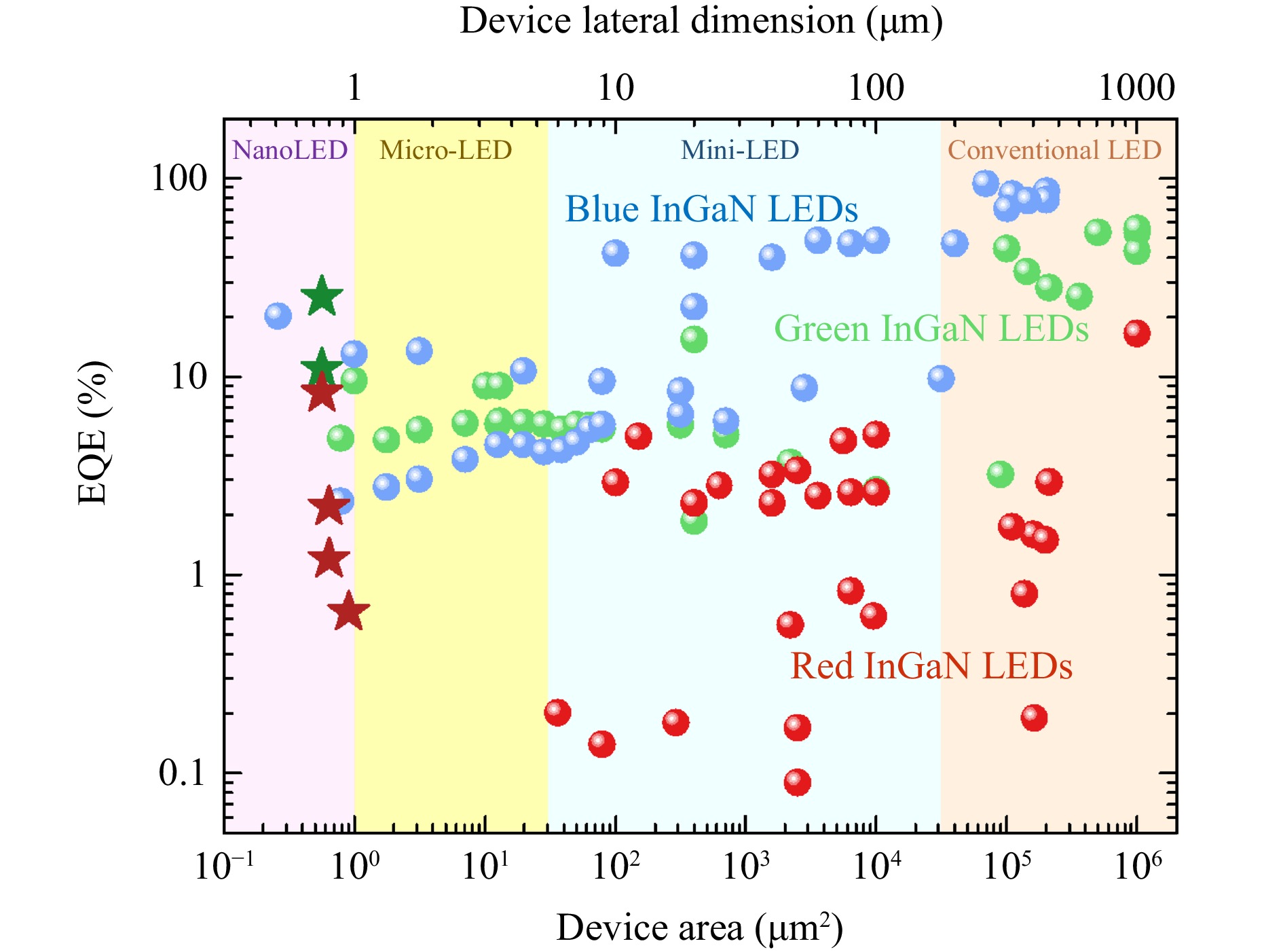
The low device efficiency has spawned great interest in improving micro-LED performance, with many research groups actively working in the field27-33. This has resulted in a marked improvement in the device efficiency for small-area blue InGaN LEDs, with most research work focusing on techniques to effectively passivate the sidewalls of the devices so as to reduce non-radiative surface recombination. D. Hwang et al. reported an external quantum efficiency (EQE) of 40.2% for a device with a size of 10 µm × 10 µm in the blue spectrum34. A high EQE of 20.2 ± 0.6% for blue micro-LEDs was reported very recently by a top-down approach, wherein a conventional multiple-quantum well epilayer LED heterostructure was etched to form nano-rods that were then passivated using an SiO2-based sol-gel35. However, the successful realization of high-efficiency small-area devices has not been replicated for green and red InGaN LEDs. A peak EQE of 14% for green micro-LEDs was demonstrated with a device size of 40 × 40 µm36. J.M. Smith et al. have studied the effect of surface recombination on device size for micro-LEDs with diameters between 1 µm and 30 µm. They measured a maximum EQE of ~7% for green micro-LEDs with device dimensions of 6 × 6 µm37. For devices with red emission, P. Li et al. have examined in detail the temperature dependent properties of red micro-LEDs with an area of 60 µm × 60 µm, and a peak EQE of 3.2%38. They have also demonstrated a red-emitting micro-LED with a tunnel junction contact, having a maximum EQE of 4.5%39. Recently, Y.M. Huang et al. reported a 6 µm × 25 µm sized red micro-LED with a peak EQE of 5.02%, with a focus for visible light communication applications40. A peak EQE of 1.75% has also been demonstrated for a device with 2 µm diameter41. The EQE of some III-nitride based LEDs from literature, of different emission colors, are plotted in Fig. 1 for varying device active areas26, 29, 32-101. The EQE of the LEDs shows a drastic reduction when the area of the LEDs becomes smaller for all wavelengths. This reduced efficiency greatly inhibits the commercialization of micro-LED technology. The causes for this efficiency cliff will be discussed in the next section.
Regarding the emission wavelength of devices, conventionally, the III-nitrides (AlInGaN) are more generally used for shorter wavelength blue-green emission, whereas the smaller bandgaps of AlInGaP alloys make them better suited for yellow-red emission. However, specifically for micro-LEDs, several factors have motivated the investigation of using InGaN to cover long-wavelength red devices as well. Firstly, the bandgaps attainable through the InGaN material system can cover the entire visible spectrum, which could enable full-color red-green-blue (RGB) devices made from a single material. It has also been shown that InGaN-based LEDs are significantly less impacted by temperature due to the better quantum-confinement of charge carriers, as compared to AlInGaP devices, which improves their usability in applications where heating can affect performance102. Finally, and most importantly, a lower surface recombination velocity has been measured in the III-nitrides, as compared to AlInGaP, making them a preferable alternative for small-area devices103, 104. This is due to the increase in the dominant effect of surface recombination for micro-LEDs especially those with dimensions < 5 µm, which have a high surface-area to volume ratio.
Instead of using a combination of III-V semiconductor materials for emitting at different wavelengths, phosphors and quantum dots have been proposed for color conversion. While this method might simplify the production of displays, there are several technological challenges. To date, color converters suffer from low conversion efficiency, poor/non-uniform color due to cross-talk, and size limitations8, 105, which greatly limit their application for micron-scale devices. While phosphors can be created with nanoscale particles, that could potentially be used in micro-LEDs, the reduced size of the particles results in a decrease of their color conversion efficiency106. Quantum-dot based color conversion technologies are a promising alternative, especially to a mass-transfer approach for micro-LED displays, however their incorporation is also complicated with an increase in fabrication steps, and hence cost. Quantum dots are also known to suffer from saturation and degradation when under illumination, which can also lead to leakage of the light that is used for exciting them, thereby affecting the output color107, 108. Furthermore, toxicity is a major concern with quantum dots, as several of the compounds used for making them are comprised of heavy metals, such as Pb and Cd9. Active research is being undertaken to address these problems, however, fundamentally, the fact that both quantum dot and phosphors involve the down-conversion of short-wavelength blue light to attain longer wavelength green and red emission means that they would be ultimately less efficient than light sources that intrinsically produce that color.
The above discussion highlights that despite their low efficiencies, the prospect of creating monolithic RGB LEDs makes III-nitride inorganic devices the foremost approach for future micro-LED display technology. This review article firstly discusses the unique challenges associated with III-nitride micro-LEDs, including their fabrication, the difficulties in attaining longer emission wavelengths such as green and red, as well as their integration into displays. We then discuss the novel nanostructure-based approach by which several of these outstanding issues can be addressed. Our work on high-efficiency green micro-LEDs is then presented, including initial Ga-polar tunnel-junction devices, to more recent high-efficiency excitonic N-polar green submicron LEDs. This is followed by our work on developing N-polar sub-micron scale red InGaN LEDs. Subsequently, the use of photonic crystals to address the color purity of InGaN micro-LEDs is considered, with a demonstration for green micro-LED devices, along with their use for creating photonic crystal surface emitting lasers. The versatility of nanostructure devices is then further exemplified through a demonstration of green-emitting devices directly on non-native silicon substrates, as well as the realization of multi-color pixels monolithically grown in a single epitaxy step. Finally, we conclude with a summary of the major roadblocks and outlook for nanostructure-based III-nitride optoelectronic devices.
-
The primary reason for the efficiency cliff, i.e., the degradation in LED efficiency with decreasing lateral dimension, is the increased surface recombination when the device areal sizes are reduced. Conventional top-down processing of III-V devices requires a plasma etch step to define the device mesas, however this also results in severe surface damage along the periphery of the mesas, forming crystal defects and dangling bonds and also introducing impurities37, 42, 49, 109. The surface defects created through this process play a major role on the carrier injection properties, especially when the ratio of surface area to volume is high, as in the case of micro-LEDs. Further, the non-radiative surface recombination depends strongly on the material properties. In this regard, the III-nitrides are more promising candidates, as compared to AlInGaP devices, for long wavelength micro-LEDs due to their significantly reduced surface recombination velocities103. The large variation in the reported surface recombination velocities is likely due to different fabrication procedures and the different In compositions of the active regions in the samples studied. The plasma etch step has a detrimental impact on the p-doped layer, where exposure to plasma results in an N-deficient near-surface region. These point defects typically compensate the Mg acceptors, resulting in a low free hole concentration that can impact the charge transport properties of the device110-114. To show the effect of plasma etching, J. M. Smith et al. studied the size-dependent characteristics of blue and green InGaN micro-LEDs. Their investigation revealed that the EQE drops off drastically when the device is scaled below 10 µm in lateral size. This study emphasized the main challenge associated with top-down micro-LEDs – mitigating the impact of plasma damage induced defects in the near-surface region.
Several methods have been investigated to recover from the plasma etch induced damage, including annealing, exposure to nitrogen plasma, wet chemical etching, and surface treatments. It has been found that thermal annealing can reduce crystallographic damage in the near-surface region, partially recovering the device characteristics115, 116. Extending the duration of the annealing was shown to have further beneficial effects on crystal quality, however it would also result in the decomposition of the active region, affecting the emission wavelength and luminescence efficiency. It was shown that through the combination of thermal annealing with a step where the etched surface was exposed to N2 plasma, the surface stoichiometry was improved and the device characteristics could be recovered117. Hydrogen plasma treatment has been shown to enhance the peak EQE by 1.4 times in InGaN-based green micro-LEDs. This was attributed to the deactivation of Mg acceptors around the device mesa, which inhibited the injection of charge carriers along the region with a high density of surface defects56. Surface treatments immediately after mesa etching have been studied, including using atomic layer deposition (ALD) for depositing a dielectric Al2O3, or an (NH4)2S treatment, which can effectively passivate surface states57, 118. Blue-emitting InGaN micro-LEDs with an EQE of ~20.2% have been obtained by sol-gel SiO2 passivation, which was shown to be over two times more effective than SiO2 deposited using plasma-enhanced ALD35. The low-temperature sol-gel deposition approach avoided exposing the device sidewalls to thermal or plasma effects that occur in ALD, thereby minimizing any additional surface or structural defect creation that could occur due to atomic reactions. Through a combination of chemical treatment and sidewall passivation, M.S. Wang et. al. reported device size-independent peak EQE of micro-LEDs119. Finally, wet etching, typically using KOH, was shown to be effective in removing leakage paths formed during the plasma etch step. It was found that the device performance could be recovered after wet etching ~50-60 nm of the semiconductor, indicating the extent of plasma damage to the crystal, however this depth would also be affected by conditions of the plasma etch120, 121. In addition, this method is not selective, attacking even non-etched regions of the device, as well as any metal contacts. However, despite these extensive studies, the efficiency of micro-LEDs fabricated utilizing the conventional top-down etching process remains quite limited, especially for green and red devices.
-
There is a large lattice mismatch between the constituent binary compounds of InGaN alloys – InN and GaN have a lattice mismatch of ~10%122. This makes it extremely difficult to grow high-quality InGaN epilayers with emission in the green and red regions of the visible spectrum, due to the tendency of InGaN to form defects and dislocations123, 124. The low miscibility of InGaN alloys also causes significant phase separation for high In content alloys, which results in broad luminescence peaks that make it hard to achieve pure red emission125. Another consequence of the lattice mismatch is that the grown InGaN epilayers would also be under a large compressive strain, and the resulting strong piezoelectric field spatially separates the electron and hole wavefunctions51. The reduced overlap of the carrier wavefunctions limits radiative carrier recombination, further reducing the internal quantum efficiency (IQE). The emission color of the generated light also depends on the injected carrier density. At low carrier injections where the piezoelectric polarization fields cause severe band bending, the emission energy is lower than the bandgap of the alloy. At higher injection currents, where the injected carriers can screen the polarization fields, thereby flattening the bands, the emission wavelength shifts closer to the bandgap. This quantum-confined Stark effect (QCSE) implies a current dependance for the emission color, limiting the applicable brightness range of practical color devices126, 127.
Various methods have been developed to enable efficient red emission of InGaN. High-efficiency large-area red and orange LEDs were demonstrated by implementing V-pits to relax compressive strain, thereby helping to increase indium incorporation80, 128, 129. The V-pits are usually formed at the start of the growth of the low temperature layer, extending through the active region. They can help enhance the injection of carriers, as holes can be transported from the semi-polar facets of the V-pit into the deeper quantum wells. With the use of this technique, an EQE of 24% was attained for a large-area 1 mm2 LED having emission at 608 nm. However, while the average size and density of V-pits can be somewhat controlled, their location cannot, which is a major detriment to their inclusion in small-area micro-LEDs, where individual devices may randomly contain a few of them.
The large compressive strain in InGaN impacts indium incorporation into the crystal lattice, making it difficult to achieve long wavelength green and red emission130, 131. Several groups have attempted to address this challenge by deliberately relaxing the strain within the active region. A thick underlying n-GaN buffer layer was shown to reduce residual in-plane stress of the InGaN active region, improving the crystal quality52, 132. This method greatly helped in red-shifting the emission wavelength, however the efficiency remained below 2%, even for larger area 400 µm × 400 µm devices. Another similar technique to relax strain involved the growth of a superlattice beneath the active region, which also assisted in increasing the In content of the InGaN active region45, 133.
Pseudo-substrates, created by selectively performing electrochemical etching of doped GaN layers to form porous layers, were shown to be an effective tool to relax epitaxial films46, 66, 134. While red micro-LEDs have been demonstrated with this method, the fabrication process is quite complex, requiring a regrowth of the LED on the substrate after it has been made porous. Further, the porous nature of the substrate creates problems with electrical stability, reliability, and thermal conduction. Utilizing this approach, micro-LEDs with areas of up to 6 µm × 6 µm were shown, with an on-wafer EQE of ~0.2%.
Recently, semi-relaxed InGaN pseudo-substrates have been investigated for the growth of the LED structure, where an InGaN layer first grown on GaN is separated from the substrate using Smart Cut™ technology, and then transferred onto a sapphire substrate with SiO2-SiO2 bonding70. The subsequent device structure growth is done on the InGaN pseudo-substrate layer, which has a lattice constant more closely matched to the red-emitting InGaN active region. The quality of the transferred pseudo-substrates and their p-type doping, however, remain obstacles affecting device performance and yield.
Strain relaxation was also achieved through the partial decomposition of an InGaN underlayer beneath the active region135-137. This method did not involve additional fabrication steps, and only used thermal annealing of an InGaN decomposition layer grown beneath a high temperature InGaN/GaN superlattice decomposition stop layer. The high temperature caused voids to form in the InGaN decomposition layer, helping to relax the InGaN/GaN superlattice, as well as the subsequent active region growth. While this technique is quite promising, the defects and surface roughness as a result of the high temperature growth and annealing are problems that need to be addressed, which have so far limited the device EQE to below 1%.
-
To date, the integration of individual, multi-color micro-LEDs into a high-resolution display has remained a major challenge. A single pixel contains at least three different color LEDs (RGB), while displays contain several million pixels. VR applications require a pixel density of at least 60 pixels per degree (PPD) to match the visual acuity of a human with 20/20 visual acuity. Practical headsets would require a field of view of at least 100 degrees, which corresponds to a 6K screen resolution. Considering that typical headsets would have dimensions of the order of 2 inches, these screens would require pixel densities in excess of 3000 PPI138. Further, glasses-like AR displays would likely require even higher densities23, 24, 138, necessitating small LED chip sizes, as shown in Table 2.
In a display, pixels are arranged in an array, and driven in either a passive or active-matrix configuration. Both configurations use row and column interconnect lines to select a line and apply the appropriate driving voltage (current) to the pixels in that line. This is done at a high frequency so that the eye perceives a single image across the display. The primary difference between the two techniques is that while the individual LEDs in a passive matrix array are switched on for a short period of time, however, the presence of a charge storage capacitor in active-matrix arrays allow for the devices to stay on until the value assigned to them is updated. This enables significantly higher brightness at similar input currents for active matrix displays. However, the additional backplane transistors needed for active-matrix displays using micro-LEDs require micro-CMOS circuitry. This is typically achieved through a transfer process. Traditional pick-and-place methods for integration would struggle to handle such large quantities of devices while maintaining high throughput, yield, and precision. Further, the large number of devices makes it imperative to develop effective methods for defect identification, testing and mitigation. While pick-and-place would remain viable in applications with low PPI requirements, for emerging technologies requiring high PPI, such as AR/VR, the placement of the devices and their yield are major challenges with pick-and-place mass transfer139.
Direct wafer-scale mass transfer can enable wafer-to-wafer or die-to-wafer assembly, greatly simplifying the fabrication process. This monolithic integration of the LEDs onto complementary metal-oxide semiconductor (CMOS) and low-temperature polysilicon (LTPS) backplanes has been demonstrated for producing screens of different sizes and resolutions140, 141. However, so far these displays have only been in a single color, with the expectation that color-converting quantum dots could be potentially integrated into them for making a full-color display.
-
Considering the challenges facing micro-LED efficiency, integration and long-wavelength operation, nanostructures offer an alternative path and solution for achieving high efficiency micro-LEDs. The bottom-up approach to growing nano or micro-LEDs precludes the need for plasma etching of the active region to define device mesas, as in the case of conventional top-down LEDs, thereby avoiding the creation of surface defects. Both metal-organic chemical vapor deposition (MOCVD) and molecular beam epitaxy (MBE) have been used for the growth of nanostructures on a variety of lattice mismatched substrates with dislocation-free crystals, greatly enhancing the quantum efficiency of charge carrier recombination3, 27, 142-162. The high surface area to volume ratio during crystal epitaxy is also beneficial for strain relaxation and promoting the incorporation of indium in InGaN layers163-165. Nanostructures have an enhanced dopant incorporation, due to strain relaxation, which is crucial to maximizing injection efficiency in LEDs166-169. The incorporation of wide-bandgap AlGaN in InGaN nanostructures also results in the spontaneous formation of a core-shell structure, with the wider bandgap material forming the shell, thereby shielding the low bandgap active region from the effects of surface recombination146.
Selective area epitaxy (SAE) of nanostructures has been demonstrated, using both MBE and MOCVD, which allows for precisely defining the dimensions, shape, morphology, and placement of the nanostructures prior to epitaxy170-176. The growth involves a precise control of growth conditions to allow crystal formation only in areas where the substrate is exposed, with no growth occurring in the mask region covering the substrate elsewhere. The morphology of the growth has been shown to depend critically on growth conditions, as well as the condition of the substrate. K. Kishino et al. studied the selective-area growth of InGaN/GaN nanowires using MBE177-181, and demonstrated multi-color (red, green, blue, yellow) pixels monolithically grown on a substrate. By varying the dimensions of the nanowires, the emission wavelengths of InGaN/GaN nanowires could be tuned through the entire visible spectrum. Their work demonstrated how the emission wavelength of nanostructures depends on their dimensions, as well as configuration in an array – where the effect of shadowing of material during epitaxy can affect composition. L. Samuelson et al., studied selective-area growth of micron-scale and smaller platelets, pyramids and nanowires using MOCVD, especially for their application in micro-LEDs182, 183. T. Wang et al. demonstrated a peak EQE of ~9% for a green LED array, grown using selective area epitaxy, wherein the diameter of individual devices was ~3.6 µm33, 44. They further demonstrated red-emitting micro-LEDs using this method with a peak EQE of 1.75%41. In addition, they monolithically integrated a high-electron-mobility transistor (HEMT) with a micro-LED, to target high-speed visible-light communication applications184. A record modulation bandwidth of 1.2 GHz was measured from the monolithically integrated bottom-up device, showcasing the possibilities of bottom-up device epitaxy and fabrication.
A schematic of the SAE process used in plasma-assisted molecular beam epitaxy is shown in Fig. 2a. Through this process, highly uniform arrays can be grown over relatively large areas, shown in Fig. 2b. The composition of the alloys can be readily tuned by adjusting the ratio of the metal fluxes for the constituent elements (In and Ga). Photoluminescence spectra from nanostructures grown using this method are shown in Fig. 2c, with emission covering the entire visible spectrum. As the incorporation of In depends strongly on the arrangement of nanostructures, due to effects such as adatom migration and flux shadowing from adjacent structures, through this method multiple different InGaN emission colors can be attained2, 177, 185.
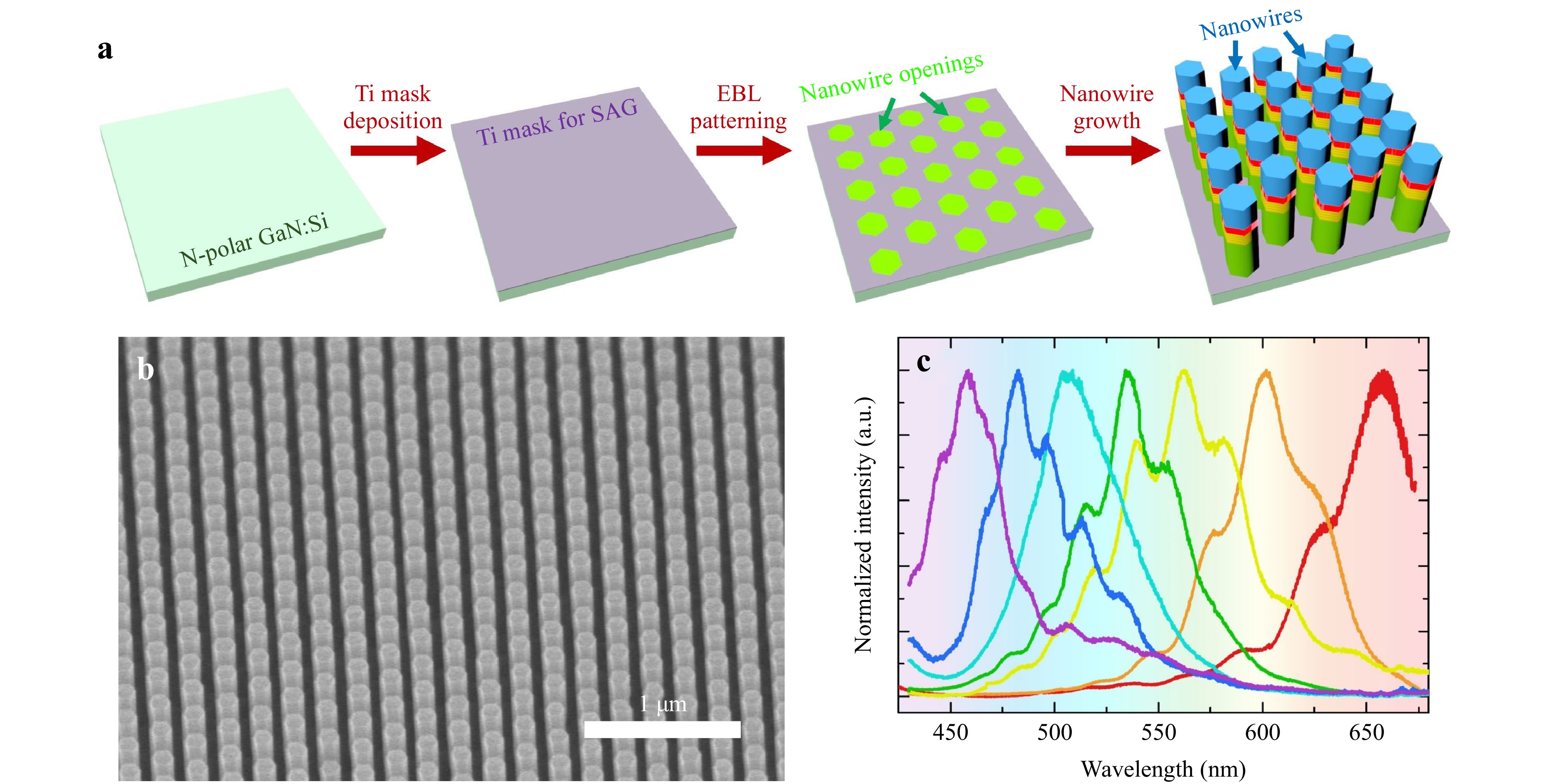
Fig. 2 a Schematic of the SAE process for the growth of nanostructures. This figure has been adapted with permission of the Chinese Laser Press, from the Ref. 65: A. Pandey et al., “Strain-engineered N-polar InGaN nanowires: towards high-efficiency red LEDs on the micrometer scale”, Photonics Research, vol. 10, no. 12, pp. 2809-2815, 2022. b SEM image of an array of nanowires grown using SAE. c PL spectra measured from various InGaN/GaN nanowire arrays covering the visible spectrum.
The arrangement of the nanostructures can also be set such that they form a photonic crystal or metasurface structure186, 187. By carefully designing the photonic crystal, the emission properties of the nanostructures formed within them can be enhanced – the light extraction efficiency can be increased, emission could be made more directional, and the emission spectral broadening can be greatly reduced. This approach has been further exploited in the design and fabrication of nanostructure-based surface emitting lasers, i.e., photonic crystal surface emitting lasers (PCSELs).
Finally, the unique growth process of nanostructures can enable their easy integration onto a variety of substrates, which could be utilized to monolithically integrate the micro-LED devices with circuitry comprising of different materials, such as silicon and SiOx188, 189.
-
Strong green emission has previously been demonstrated from nanowires grown using plasma-assisted molecular beam epitaxy (PA-MBE)100, 142, 158, 190, 191. To fabricate micro-LED devices, nanowire arrays were patterned on Ga-polar GaN-on-sapphire substrates for SAE using a thin 10 nm Ti mask layer100. Electron beam lithography was used to etch vias defining the injection openings into this layer. Then, using optimized growth conditions for high selectivity of growth (growth only in the openings where GaN is exposed), a multiple quantum disk InGaN/AlGaN LED was grown. Following the active region, a p-AlGaN electron blocking layer was grown to reduce electron overflow. High resolution TEM images show that this AlGaN layer, along with the AlGaN barriers in the active region, form a shell around the InGaN active region. The presence of the high bandgap Al-rich shell greatly reduced the impact of surface recombination on the nanostructures, which should already be low due to the absence of any plasma etching steps. An n++/p++ GaN tunnel junction contact layer was also incorporated above the p-GaN layer to improve the hole injection to the active region.
To fabricate the nanowires into micro-LEDs, nanowire arrays were first filled with Al2O3 deposited by ALD, which was then etched back to reveal the top of the nanowires. Plasma-enhanced chemical vapor deposition (PECVD) was then used for depositing a thick SiO2 insulation layer. Stepper lithography was used to etch injection vias into the SiO2 layer to define the active area of the devices. Finally metal contacts were deposited and annealed. Fabricated devices exhibited relatively good I-V characteristics, and strong green electroluminescence (EL), as shown in Fig. 3a. As the growth of the InGaN was primarily along the semi-polar facets of the Ga-polar nanowires, the reduced polarization fields resulted in a small wavelength shift with injection current, with EL spectra at different currents plotted in Fig. 3b. For micro-LEDs having an area of 3 µm × 3 µm, a maximum EQE of ~5.5% was measured at a current density of ~3.4 A/cm2, shown in Fig. 3c. Furthermore, as the micro-LEDs were fabricated in arrays of nanowires, with individual nanowires having identical emission and morphology, there were relatively small variations in the normalized EQE of different area devices formed in the same array, shown in Fig. 3d.
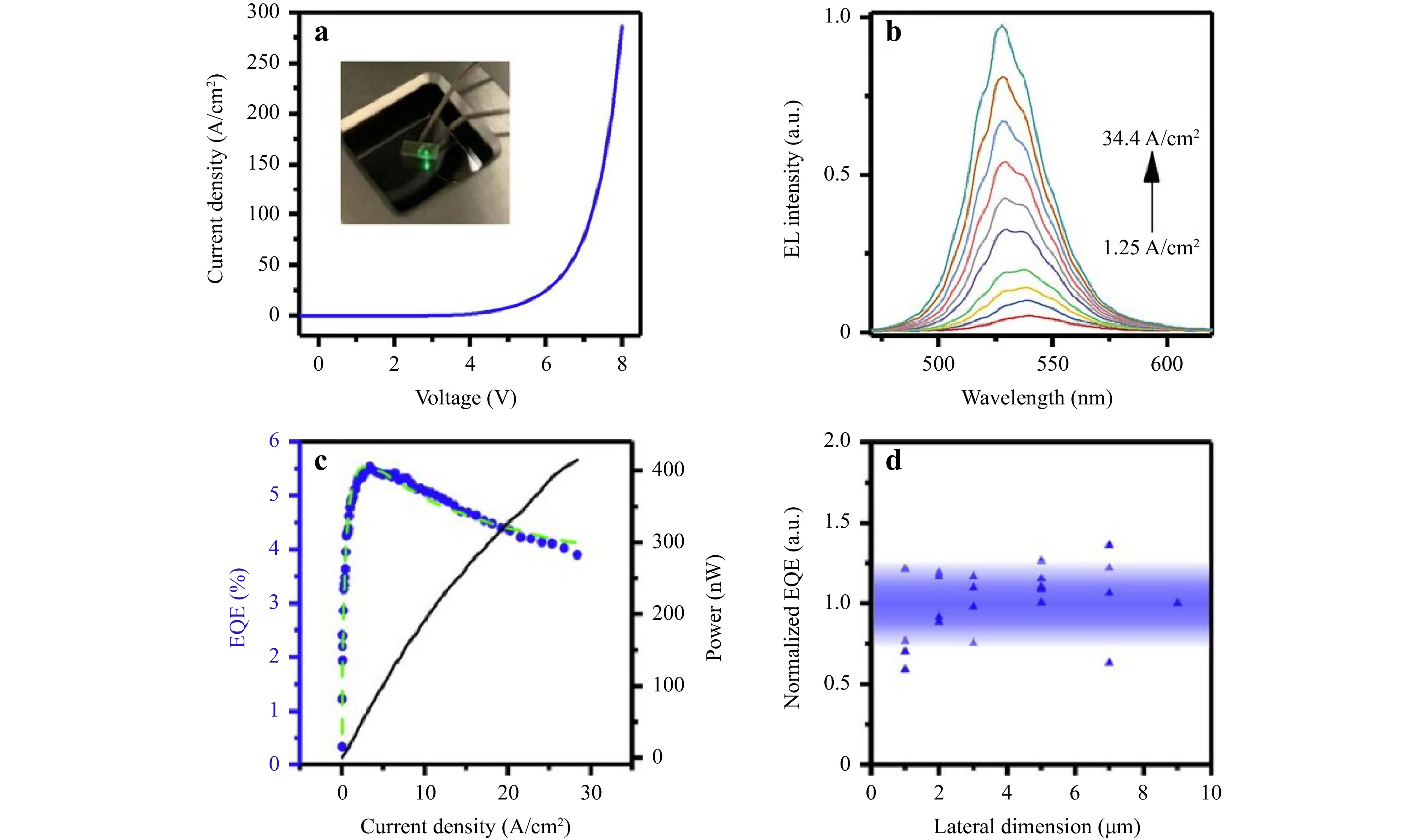
Fig. 3 a J-V of a fabricated green-emitting TJ micro-LED. The inset shows a device under operation. b EL spectra measured at different injection currents for the device. c EQE and output power vs. current density for a high-efficiency green micro-LED. d Normalized EQE vs lateral dimension for different devices. This figure has been reprinted from Ref. 100: X. Liu et al., “High efficiency InGaN nanowire tunnel junction green micro-LEDs”, Applied Physics Letters, vol. 119, no. 14, p. 141110, 2021., with the permission of AIP Publishing.
-
Recently N-polar nanostructure-based LEDs have gained significant attention. Previous work on bottom-up nanostructure micro-LEDs was primarily aimed toward materials with metal polarity. In metal-polar devices with conventional structures having the p-type layer on top of the active region, the polarization fields inhibit carrier injection to the active region, resulting in severe electron overflow/leakage and nonradiative parasitic recombination outside of the device active region that diminishes device efficiency146, 149, 192-194. Further, the tip of metal-polar nanowires has a faceted morphology that complicates device fabrication, unlike N-polar nanowires that have flat top surfaces195. The reversed polarization fields present in N-polar devices are also beneficial to charge carrier injection and can greatly improve device emission characteristics at high current injection192. N-polar InGaN has been shown to have a higher decomposition temperature than its metal-polar counterpart, which can make higher growth temperatures possible, resulting in improved material quality196, 197.
Taking advantage of these benefits, high efficiency N-polar green nanowire sub-micron scale LEDs have been demonstrated. To ensure the N-polarity of the grown nanowires, an N-polar GaN substrate was used for seeding the initial nanowire nucleation. Over a base n-GaN segment, a six-period InGaN quantum disk/AlGaN barrier active region was grown, followed by a p-type AlGaN electron blocking layer and a p-GaN contact layer. A schematic of the nanowires and their structure is shown in Fig. 4a. SEM images of the nanowires following growth confirm the uniform morphology and flat top surface, shown in Fig. 4b. Similar to studies on Ga-polar structures, an AlGaN shell was formed, protecting the active region from surface recombination. This was confirmed with elemental mapping of the active region, presented in Fig. 4c, for In and Al. High resolution atomic-scale images shown in Fig. 4d also confirmed the N-polarity of the grown nanowires.
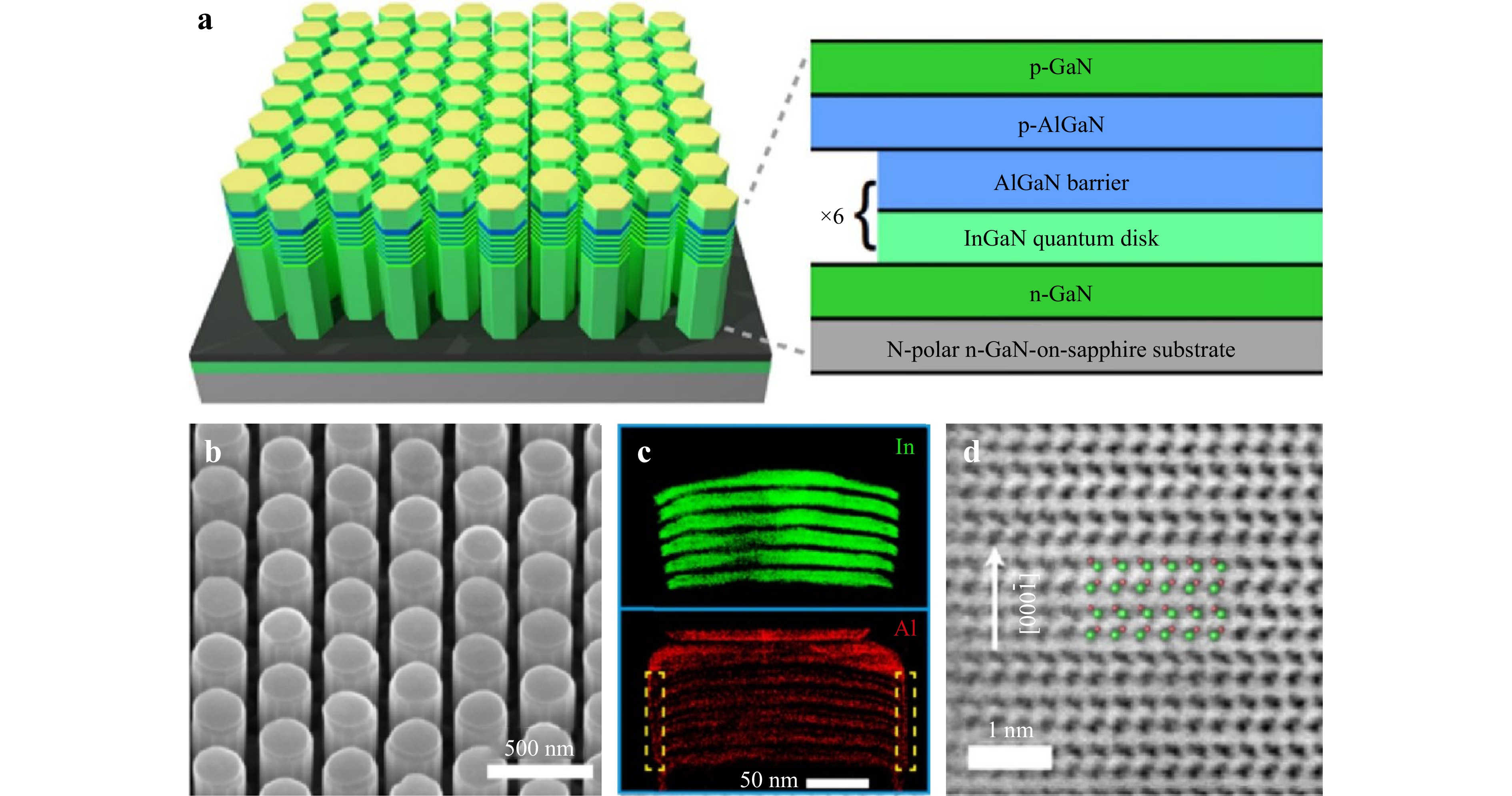
Fig. 4 a Schematic and device structure of N-polar green micro-LEDs. b SEM image of an array of InGaN/GaN nanowires. c Elemental mapping of the active region in the nanowires for In and Al. d High resolution atomic scale image of the nanowire, confirming the N-polar orientation. This figure has been reproduced with permission of the Chinese Laser Press, from the Ref. 99: X. Liu et al., “N-polar InGaN nanowires: breaking the efficiency bottleneck of nano and micro LEDs”, Photonics Research, vol. 10, no. 2, pp. 587-593, 2022.
To fabricate devices using the above nanowire arrays, they were planarized using Al2O3 deposited by ALD and SiO2 deposited by PECVD. Lithography was used to define injection vias in the insulating SiO2 layer at the sub-micron scale. The inset of Fig. 5a shows an SEM image of the injection window for a sub-micron device which consisted of only four nanowires. Fabricated devices showed negligible reverse leakage current, as plotted in Fig. 5a. The turn-on voltage of the device could be reduced in future work by optimizing the device fabrication process. Fig. 5b plots the EL spectra from the device at different injection currents. The main emission peak is at ~530 nm, and it remained stable with varying injection current. Green emission was observed from a sub-micron device under operation, even under room-light illumination, shown in the inset of Fig. 5b. The variation of the measured output power with injection current is plotted in Fig. 5c, and the EQE vs. injection current in Fig. 5d. The EQE reached a maximum of ~11% at a relatively low current density of 0.83 A/cm2. The low current corresponding to the peak EQE suggests that the non-radiative SRH recombination is minimal in the devices . This confirmed both the excellent material quality, as well as the benefits of the bottom-up fabrication process which avoided exposing the active region to plasma damage.
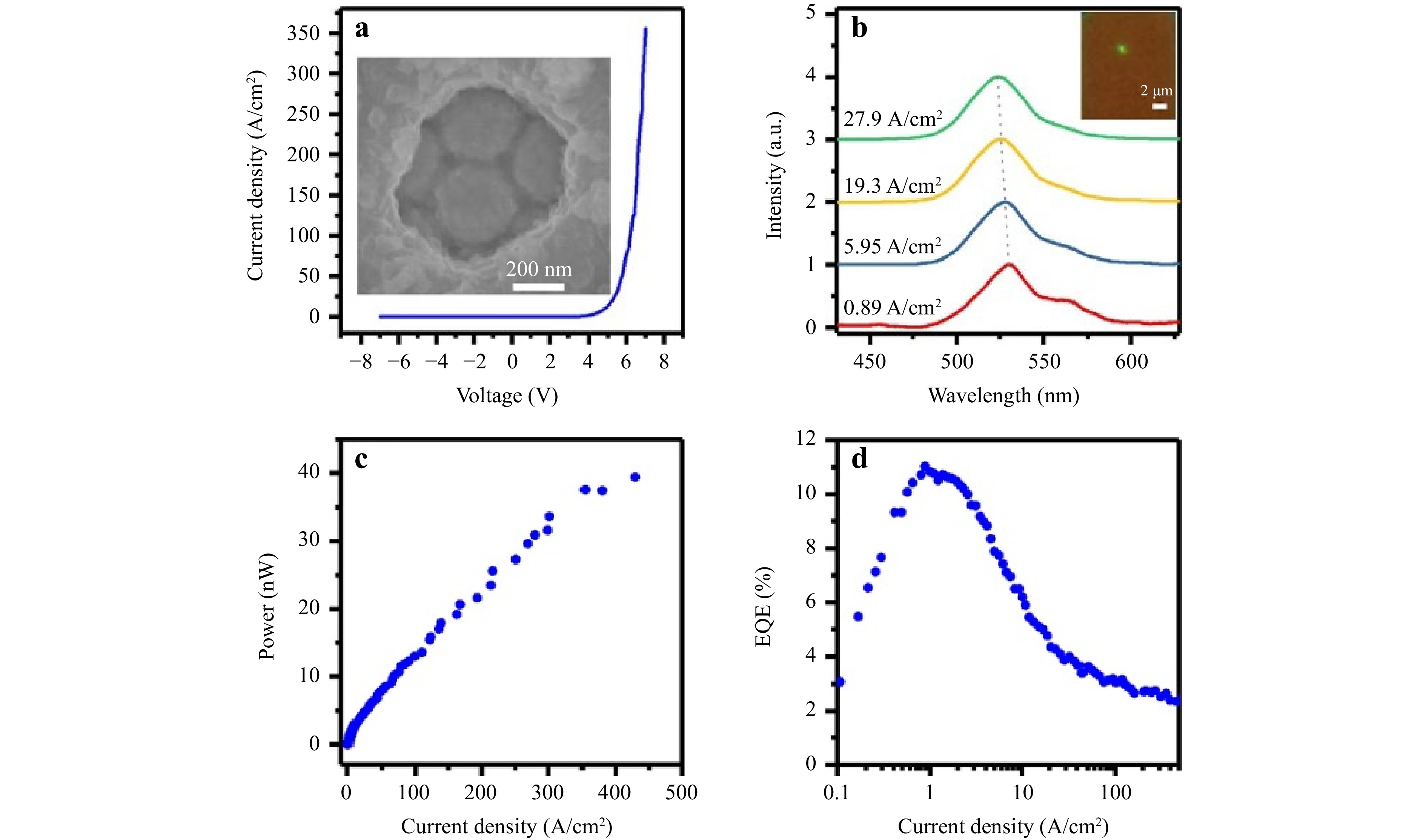
Fig. 5 a J-V of a fabricated N-polar green-emitting submicron scale LED. The inset shows an SEM image of an injection window that forms a submicron device. b EL spectra from a submicron LED measured at different injection currents. The inset is an optical microscope image of an operating device under room light illumination. Plots of measured c output power and d EQE with current density for the submicron LED. This figure has been reproduced with permission of the Chinese Laser Press, from the Ref. 99: X. Liu et al., “N-polar InGaN nanowires: breaking the efficiency bottleneck of nano and micro LEDs”, Photonics Research, vol. 10, no. 2, pp. 587-593, 2022.
The structure of the quantum wells formed in the nanowire are also of extreme interest, as previous work has shown that InGaN insertions in N-polar GaN nanowires tend to form a faceted surface to facilitate strain relaxation27, 198-200. These facets are formed along the semi-polar planes, with different indium compositions, resulting in a complex geometry for the active region. The benefits of strain relaxation and highly confined InGaN active regions along the facets can localize charge carriers, promoting excitonic recombination, potentially further increasing the peak EQE of the device. This advantage has been harnessed recently to realize high efficiency excitonic green submicron scale nanowire LEDs98. Fig. 6a-c show TEM images of nanowires, along with high resolution images at the center and the facets for the InGaN active region within the nanowire. Elemental maps of the Ga and In ratio at different positions along the radius of the nanowire showed an increase in indium composition for the growth along the semi-polar facets. The extent of faceting is a consequence of the growth conditions and the dimensions of the nanowires, which must be controlled to tune the emission properties from the facets177, 198. The high indium composition and low strain in the faceted InGaN regions200 is essential for promoting carrier recombination within them, especially at low current injection. Further, these factors also improve the electron-hole wavefunction overlap, increasing the exciton oscillator strength and binding energy in the faceted regions201-203. The improved excitonic recombination can greatly reduce nonradiative Shockley-Reed-Hall recombination and therefore enhance device efficiency.
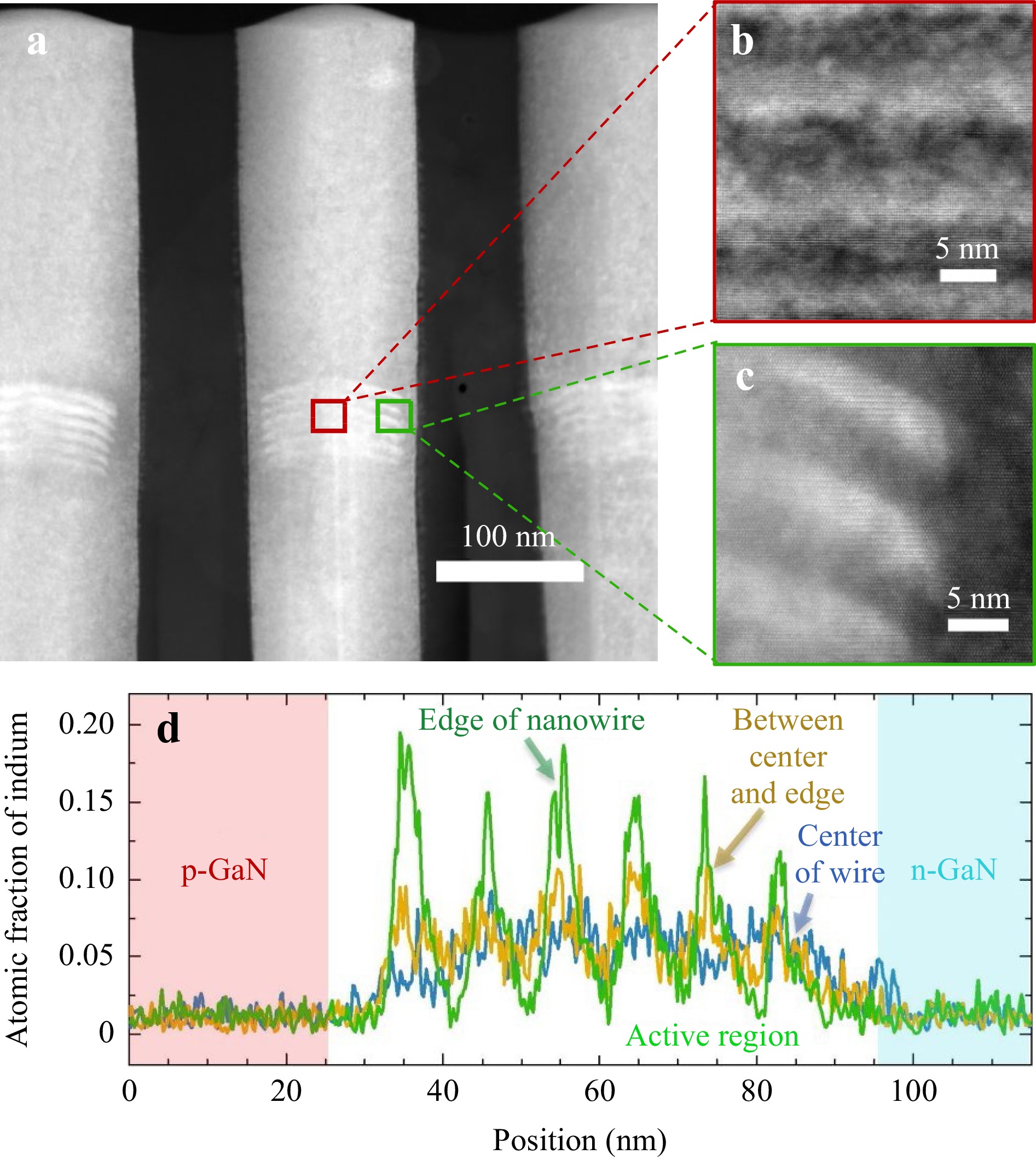
Fig. 6 a STEM HAADF image of nanowires comprising an excitonic micro-LED. High-resolution HAADF images of the InGaN quantum disk active region from b the center of the nanowire and c near the sidewalls of the nanowire. d Atomic fraction of indium plotted along the growth direction in different regions of the nanowire. This figure has been reprinted with permission from Ref. 98: A. Pandey et al., “An Ultrahigh Efficiency Excitonic Micro-LED”, Nano Letters, vol. 23, no. 5, pp. 1680-1687, Mar 8, 2023. Copyright 2023 American Chemical Society.
These nanowires were fabricated into submicron scale devices using the process described above. The inset of Fig. 7a shows a submicron injection window, similar to that used in the device. The designed area of the submicron LED is ~750 nm × 750 nm. The J-V characteristic of the fabricated device is shown in Fig. 7a, with low reverse current leakage. The inset of Fig. 7b shows a camera image of a submicron device at high injection current, with bright green emission. A microscope image of the device operating at low injection is shown in Fig. 7c. The variations of EQE and WPE vs. current density are plotted in Fig. 7b, c, respectively. The excitonic nature of recombination promoted a high efficiency, especially at low current injections, as measured here with a peak EQE of 25.2%. The corresponding peak WPE was 20.7%, suggesting efficient carrier injection. At higher injection currents, when the carrier density exceeds the Mott density, Coulombic screening would cause the excitons to disassociate204 and free carrier (electron and hole) recombination from the central region of the nanowire (away from the facets) would dominate, and this effect contributes to the sharp decline of efficiency above 0.3 A/cm2.
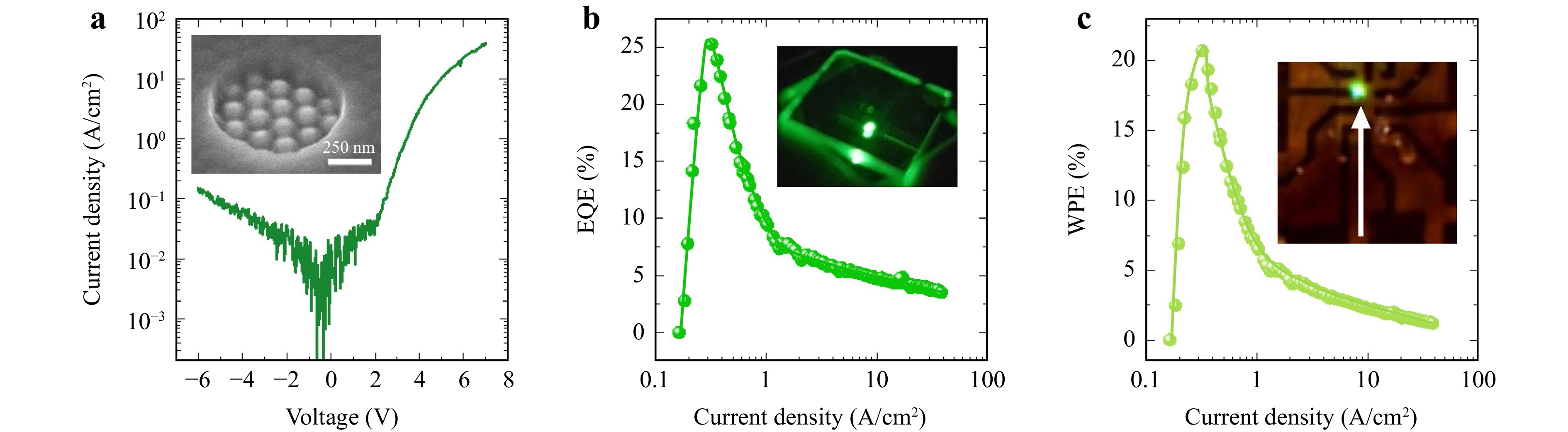
Fig. 7 a J-V characteristic of the excitonic green micro-LED. The SEM image in the inset shows a submicron device injection window. b EQE and c WPE vs. current density for the device. The inset of b shows a camera image of an operational device at high current injection. The inset of c shows an optical microscope image of a device at low current injection. This figure has been reprinted with permission from Ref. 98: A. Pandey et al., “An Ultrahigh Efficiency Excitonic Micro-LED”, Nano Letters, vol. 23, no. 5, pp. 1680-1687, Mar 8, 2023. Copyright 2023 American Chemical Society.
This study brought excitons to the foreground in the search for routes to overcome the efficiency bottleneck of a broad range of nanoscale optoelectronic and quantum devices including LEDs, lasers, detectors, and single photon source, to name a few. It also opens up another avenue in tuning the dimensions of the grown nanowires – which are crucially responsible for the extent of strain relaxation and faceting, thereby affecting excitonic recombination.
-
As N-polar green emitting submicron LEDs showed excellent performance, the next step was extending them towards longer wavelength in the red64. Firstly, a relatively thick InGaN segment was used to minimize the QCSE. An in-situ anneal at a temperature 50°C higher than the growth temperature of the InGaN segment was incorporated to improve the emission intensity of the active region. Such an anneal step had previously been demonstrated to greatly enhance the luminescence by reducing the density of defects205, 206. Here, an order of magnitude increase in the photoluminescence emission was measured from the device active region using the in-situ anneal, as shown in Fig. 8a. TEM of grown nanowires in Fig. 8b showed a thick InGaN active region, and elemental mapping nanowires in Fig. 8c, plotted along the growth direction, confirmed the presence of graded interfaces, suggesting that there was significant In inhomogeneity due to effects such as composition pulling and In diffusion. This would explain the broad FWHM of the emission.
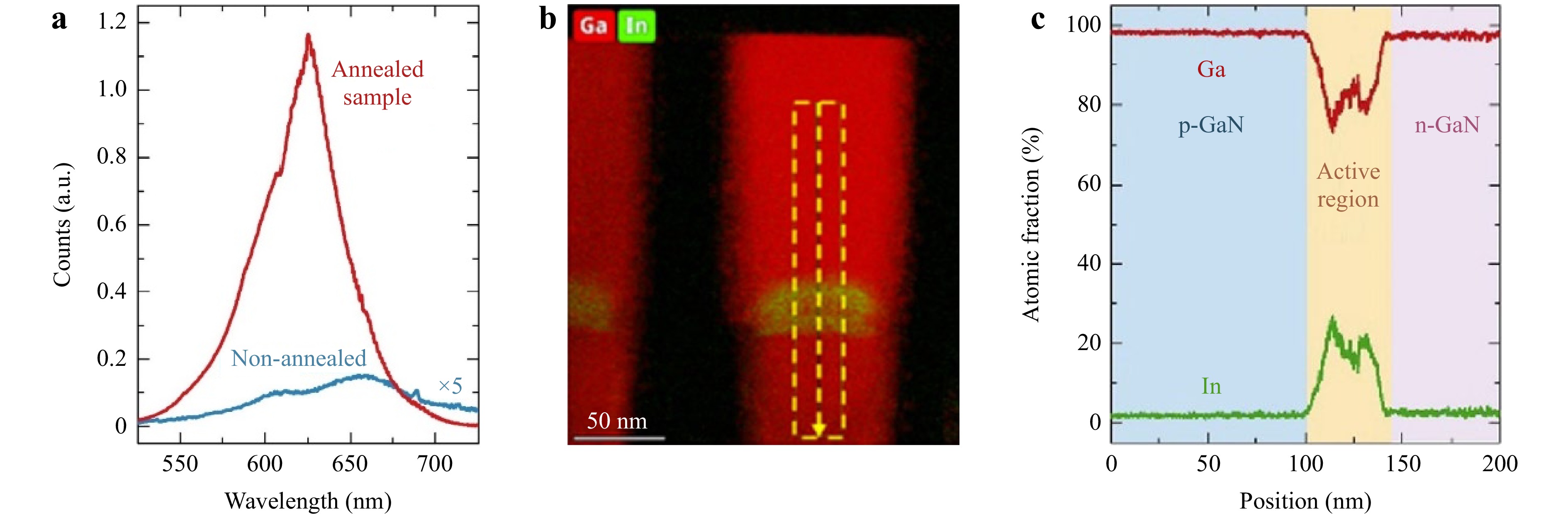
Fig. 8 a PL spectra for a non-annealed sample and a sample with in-situ annealing. b TEM image showing the location of Ga and In atoms in the nanowire crystal. c Plot of the elemental map of In and Ga along the growth direction. This figure has been reproduced with permission of the Chinese Laser Press, from the Ref. 64: A. Pandey, Y. Malhotra, P. Wang, K. Sun, X. Liu, and Z. Mi, “N-polar InGaN/GaN nanowires: overcoming the efficiency cliff of red-emitting micro-LEDs”, Photonics Research, vol. 10, no. 4, pp. 1107-1116, 2022.
Red-emitting micro-LEDs were then fabricated, following the process as the green N-polar submicron devices. The J-V characteristics of a 750 nm × 750 nm area device are plotted in Fig. 9a, showing a sharp turn-on at ~2.5 V, with negligible reverse leakage current. Injection-dependent EL spectra for the device have been plotted in Fig. 9b, confirming the peak emission at ~620 nm at low injection currents. At higher injection currents a blue-shift was seen in the EL peak, as is expected due to the QCSE. The EQE vs. current density has been plotted in Fig. 9c, showing a peak of ~1.2% at a current density of 0.5 A/cm2. This was the first demonstration of a submicron scale red micro-LED, and the efficiency attained was significantly better than conventional top-down fabricated micro-LEDs with areas of 100 µm2 or smaller at the time of this work.
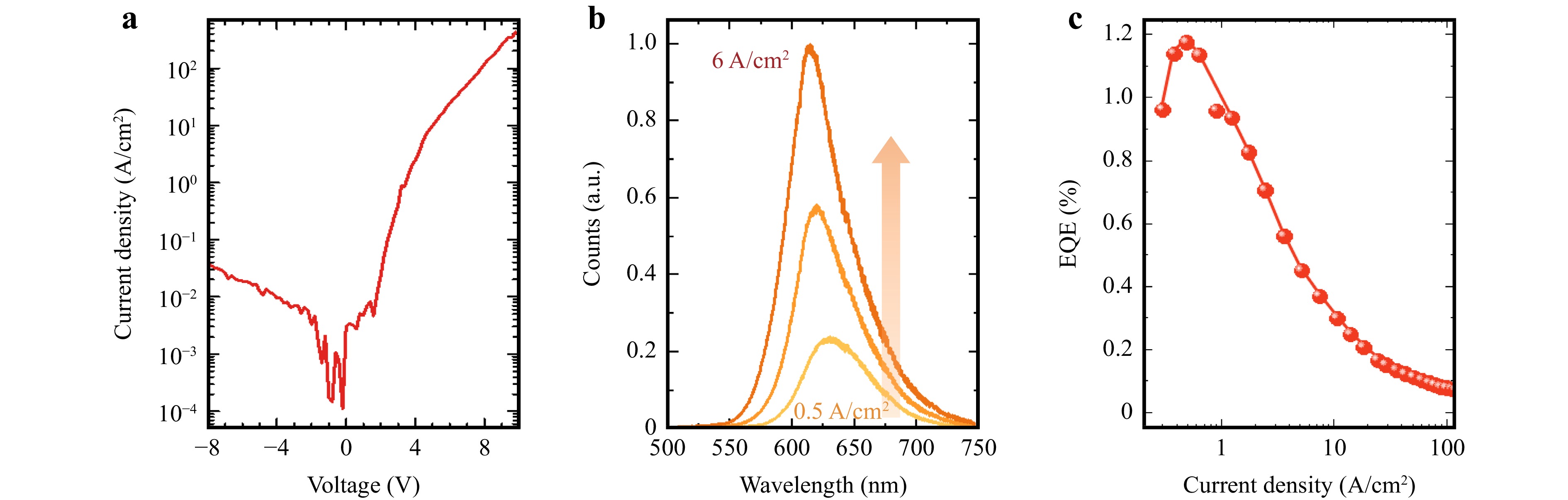
Fig. 9 a J-V characteristics of a red submicron LED. b EL spectra of the InGaN/GaN micro-LED measured at different injection currents. c Variation of the EQE vs. injection current density. This figure has been reproduced with permission of the Chinese Laser Press, from the Ref. 64: A. Pandey, Y. Malhotra, P. Wang, K. Sun, X. Liu, and Z. Mi, “N-polar InGaN/GaN nanowires: overcoming the efficiency cliff of red-emitting micro-LEDs”, Photonics Research, vol. 10, no. 4, pp. 1107-1116, 2022.
To further improve the nanowire-based red micro-LEDs, an InGaN/GaN short-period superlattice (SPSL) was incorporated beneath the device active region65. Previous work has shown the benefits in strain relaxation and achieving longer wavelength emission by incorporating a SPSL in conventional planar quantum well devices207-209. The benefits of the SPSL layer for strain relaxation can be further enhanced with the use of nanostructures, due to the increased surface area to volume ratio, thereby allowing for more efficient red emission.
A four-period InGaN (8 nm)/GaN (8 nm) SPSL was included in InGaN/GaN nanowires through which it was possible to significantly red-shift the PL emission from an InGaN dot active region, as shown in Fig. 10a. Micro-LED devices fabricated on nanowires with the incorporated SPSL showed excellent J-V characteristics, seen in Fig. 10b. The variation of the EQE and WPE with current density for the submicron LED is plotted in Fig. 10c. The EQE reached a peak value of ~2.2%, and the WPE peaked at 1.7%. The EL spectra for the devices, plotted in Fig. 10d, showed a peak emission ~630 nm. While lower injection spectra were dominated by the emission from the InGaN dot, at higher currents the SPSL also contributed a green-yellow emission peak that could distort the spectral purity of the emitted light.
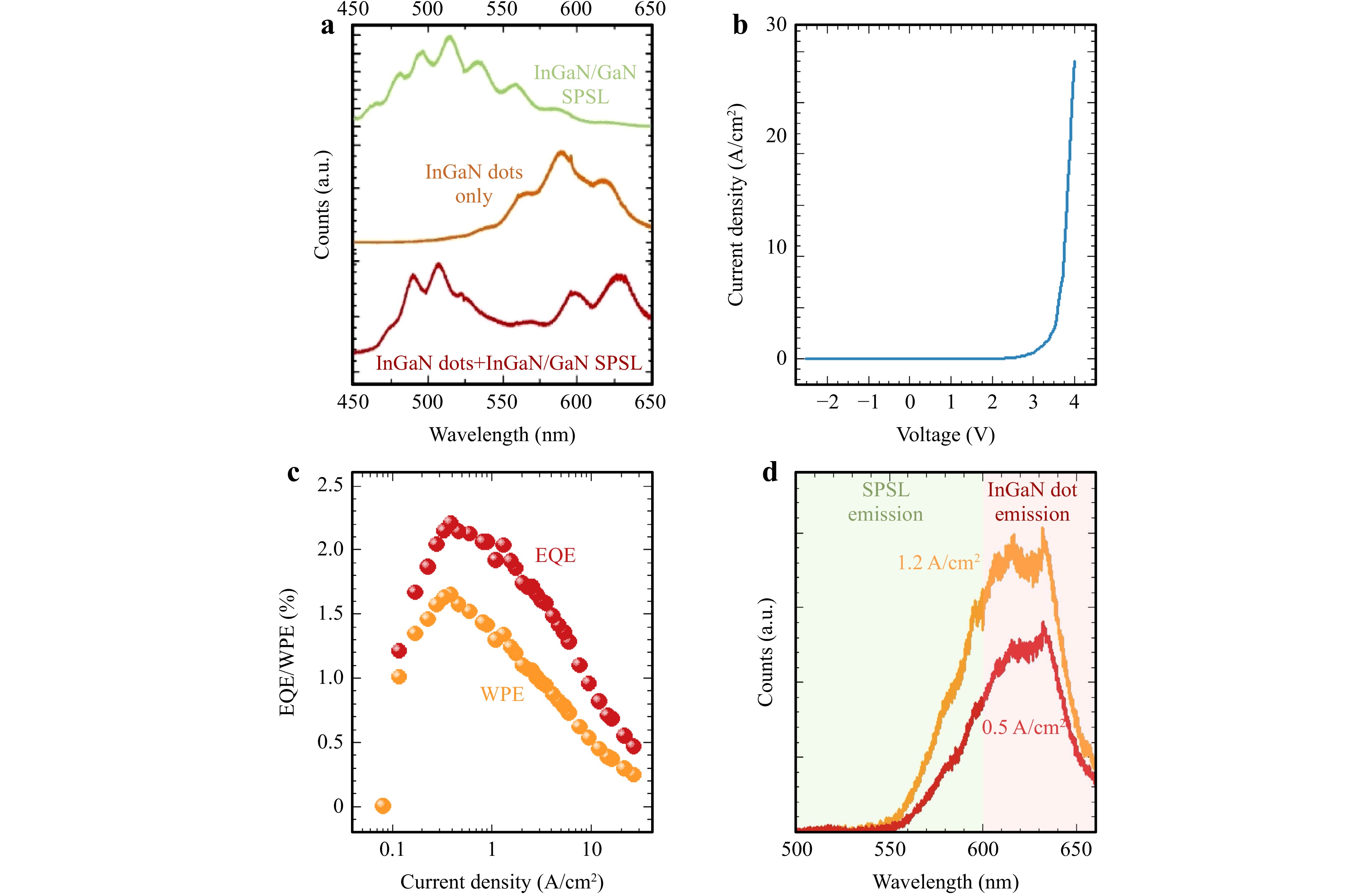
Fig. 10 a PL spectra measured for samples containing only the InGaN/GaN SPSL, only the InGaN dot, and both the SPSL and InGaN dot. b J-V characteristics and c current-dependent EQE and WPE of a red submicron LED with an InGaN/GaN SPSL incorporated beneath the active region. d EL spectra of the InGaN/GaN micro-LED measured at different injection currents. This figure has been reproduced with permission of the Chinese Laser Press, from the Ref. 65: A. Pandey et al., “Strain-engineered N-polar InGaN nanowires: towards high-efficiency red LEDs on the micrometer scale”, Photonics Research, vol. 10, no. 12, pp. 2809-2815, 2022.
There remains significant room for performance improvement for these red micro-LEDs. The devices shown here have relatively high turn-on voltages and low WPE, which limits their practical use. To tackle these problems, further improvement and tuning of the device is in progress, with an emphasis on improving the p-doping within the GaN contact layer, as well as by including an electron-blocking layer and tunnel junction in the device heterostructure.
-
While high-efficiency long-wavelength InGaN-based micro-LEDs have been demonstrated, their spectral purity has remained a challenge125. These devices typically have large full-width half maximum (FWHM) of the emission due to the inhomogeneous In distribution as a result of phase separation, composition-pulling, local In-rich clusters and inter-diffusion of In between the InGaN active region and the surrounding layers. The QCSE also causes a current dependence of the emission peak, resulting in large shifts of emission wavelength as the device is operated at higher currents. To address these problems, the use of photonic crystal arrays has been demonstrated to tune the emission properties of devices by forming optical microcavities71, 186, 210. The Purcell effect within such photonic crystals can further increase the IQE of the desired emission186. Utilizing such photonic crystals, it has been shown that the emission can be significantly narrowed to a few nanometers in wavelength178, 186, 210 thereby greatly enhancing the emission from selected optical resonance modes.
The dimensions, spacing and arrangement of the nanostructures that form a photonic crystal play a direct role in the emission properties. Fig. 11a shows a schematic of a hexagonal array of nanowires with their reciprocal lattice vectors. Fig. 11b plots the simulated photonic band structure of an InGaN/GaN nanowire photonic crystal, having an emission wavelength λ = 505 nm, lattice constant a = 250 nm and lateral dimension d = 0.85a. The Γ point in the photonic band structure corresponds to zero group velocity of light, which is necessary for creating a resonance mode. Fig. 11c shows the calculated profile of the electric field profile for a nanowire array having a lateral dimension of 5 µm. TM-polarized light with electric field parallel to the c-plane of the nanowire crystals dominated the band-edge mode. Through further design optimization, effective guiding of the light mode has also been demonstrated using smaller arrays of nanowire-based photonic crystals186, 211.
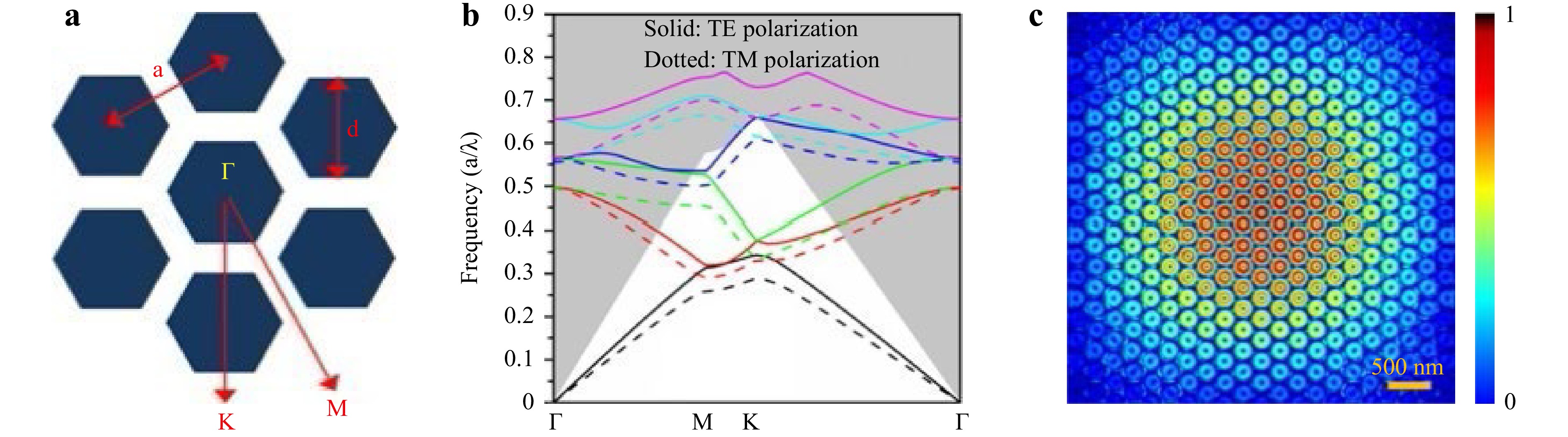
Fig. 11 a Schematic of a nanowire photonic crystal array, with the lattice constant a, nanowire diameter d, and the reciprocal lattice vectors labelled. b Simulated photonic band structure for a 2D hexagonal array of nanowires designed for an emission wavelength λ = 505 nm, a = 250 nm and d = 212.5 nm. c Electric field profile of the band edge mode calculated by 3D finite-difference time-domain method for a 5 µm × 5 µm nanowire array having λ = 505 nm. This figure is reprinted with the permission of John Wiley and Sons, from the Ref. 186: Y. H. Ra, R. T. Rashid, X. Liu, J. Lee, and Z. Mi, “Scalable nanowire photonic crystals: Molding the light emission of InGaN”, Advanced Functional Materials, vol. 27, no. 38, p. 1702364, 2017.
Photonic crystals have also been incorporated in micro-LEDs creating photonic nanocrystal (PhNC) devices210. The EL spectra for a 3 µm × 3 µm PhNC micro-LED showed a stable emission peak at ~548 nm over nearly four orders of magnitude variations of injection currents, illustrated in Fig. 12a186, 210, 212, which showed the successful mitigation of the impact of the QCSE-related blue-shift in emission45, 46, 58, 66. A relatively low efficiency droop of only ~30% was measured up to an injection current of 200 A/cm2, shown in Fig. 12b.
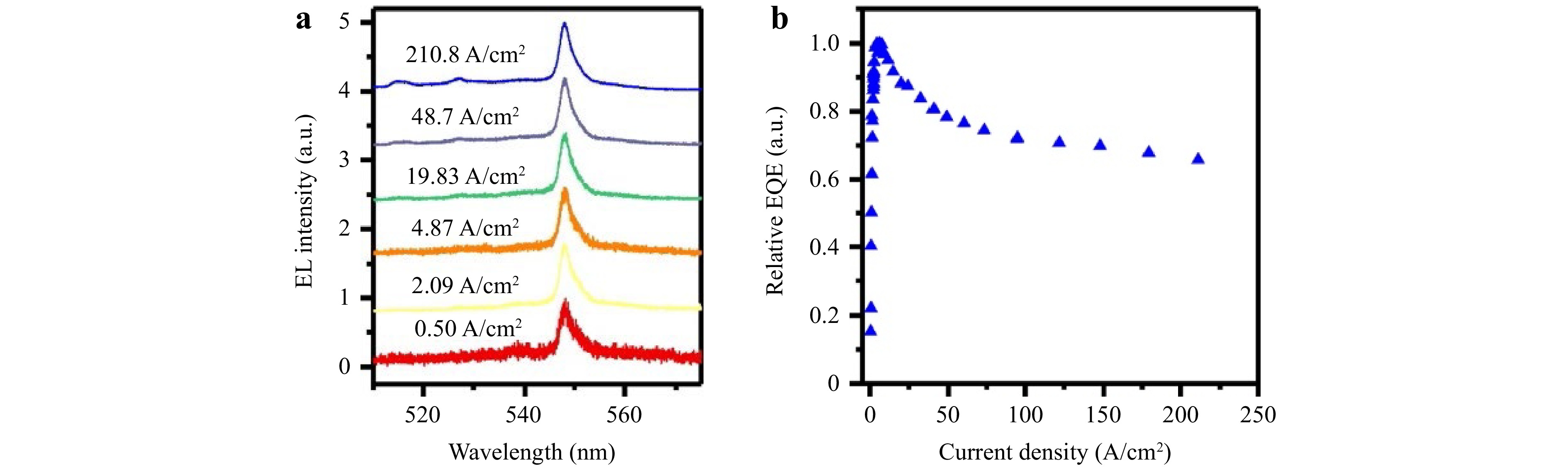
Fig. 12 a EL spectra of a PhNC micro-LED with different injection currents. b Relative EQE of the PhNC micro-LED versus injection current. This figure is reprinted from Ref. 210: X. Liu, Y. Wu, Y. Malhotra, Y. Sun, and Z. Mi, “Micrometer scale InGaN green light emitting diodes with ultra-stable operation”, Applied Physics Letters, vol. 117, no. 1, p. 011104, 2020, with the permission of AIP Publishing.
-
Dense, small-area lasers are of interest for applications including visible light communication, data storage and biosensing187, 213, 214. Photonic nanocrystal-based devices can also be extended for creating surface-emitting lasers which can be used for the aforementioned purposes212. Typical vertical-cavity surface-emitting lasers (VCSELs) require high quality dielectric Bragg reflectors (DBRs), which is a complex task considering the lattice mismatch between III-nitride layers and the relatively small difference in dielectric constant215-217. This can be avoided in photonic crystals, where the photonic band edge resonant effect allows the formation of standing waves211, 212 in nanocrystal surface-emitting lasers (NCSELs). Fig. 13a schematically depicts a green-emitting NCSEL, with the inset containing optical microscope images of a fabricated laser diode when switched off and under operation. Fabricated NCSELs showed a turn-on voltage of ~3.3 V at room temperature, with the J-V curve plotted in Fig. 13b. The semi-log scale plot in the inset confirmed low leakage current for the device under reverse bias. The EL spectra at different injection currents, measured under continuous-wave bias, are shown in Fig. 13c. At lower injection currents a broad emission peak was seen, however as the current increased, a lasing peak at ~523.1 nm began to dominate the spectrum with a narrow linewidth. The output power of the laser is plotted against the injection current in Fig. 13d, with a threshold current Jth ~400 A/cm2, that is significantly lower than conventional III-nitride VCSELs187, 218-222. Fig. 13d, f plot the FWHM and wavelength, respectively, of the lasing peak against injection current. As the injection crossed the lasing threshold, there was a sharp reduction in the FWHM from ~30 nm to ~0.8 nm. The lasing peak position showed little variation with increasing injection current and remained stable at ~523.1 nm above threshold.
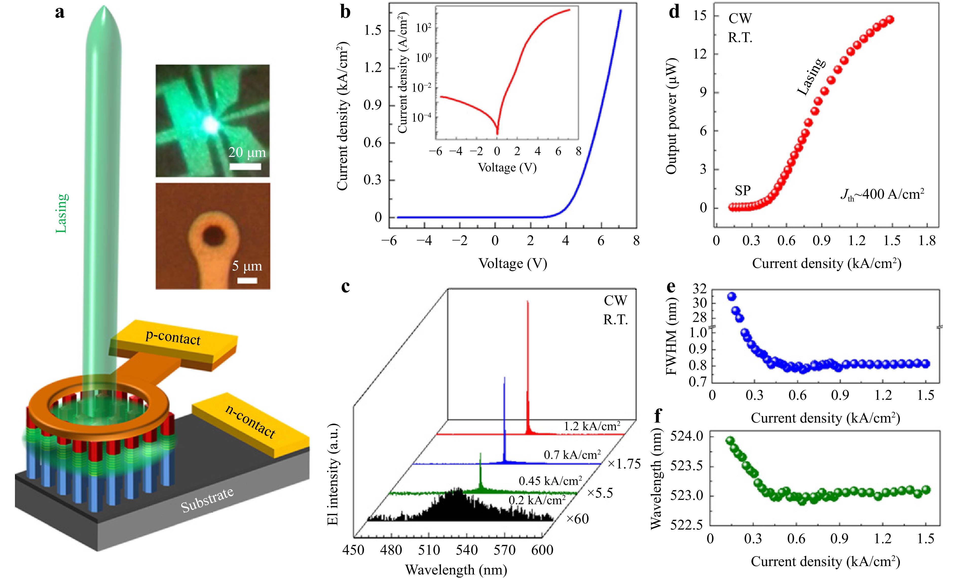
Fig. 13 a Schematic of an InGaN/GaN NCSEL. Optical microscope images of a green NCSEL under operation and when off are shown in the inset. b J-V characteristics of the green NCSEL, with a semi-log scale plot of the J-V curve in the inset. c Injection-dependent EL spectra measured at different injection currents under CW bias at room temperature. d Output power vs. injection current of the NCSEL, showing a threshold current of ~400 A/cm2. Plots of e spectral linewidth and f peak wavelength with injection current. This figure is from Ref. 212: Y.-H. Ra, R. T. Rashid, X. Liu, S. M. Sadaf, K. Mashooq, and Z. Mi, “An electrically pumped surface-emitting semiconductor green laser”, Science Advances, vol. 6, no. 1, p. eaav7523, 2020. © The Authors, some rights reserved; exclusive licensee AAAS. Distributed under a CC BY-NC 4.0 license http://creativecommons.org/licenses/by-nc/4.0/”. Reprinted with permission from AAAS.
This work showcased the extreme versatility of the selective area growth method for the realization of micron-scale or smaller optoelectronic devices. The measured threshold current density is significantly lower than conventional planar devices operating at a similar emission wavelength. The selective area growth of the photonic crystal also allows lasing without the presence of a distributed Bragg reflector (DBR) – a thick, multi-layer structure that is quite complex to grow with high quality – for the III-nitrides. While the severe heating effect limited high-power operation of this device, proper packaging and thermal management can greatly benefit its performance for potential applications in projectors, optical storage and communication, as well as displays.
-
As nanostructures can be grown to be nearly defect-free on a variety of substrates, even those with a large lattice mismatch, this opens up an avenue for the direct integration of micro-LEDs with their back-plane circuitry. Green-emitting N-polar nanowire micro-LEDs with stable operation were demonstrated on silicon substrates, showing stable emission by engineering the strain and polarization within the active region, which is comprised of InGaN quantum wells and AlGaN barriers223. An SEM image of the grown nanowires is shown in Fig. 14a. The AlGaN barrier in the active region of the nanowires formed a shell structure around the InGaN quantum well active region, shown in the TEM images in Fig. 14b, c. This thin AlGaN shell minimized the impact of surface recombination on the InGaN quantum wells. Further, the use of AlGaN barriers induced a tensile strain within the grown layers, that compensated for the compressive strain in the InGaN layers. The strain compensation promoted In incorporation within the nanowires and also assisted in screening of the QCSE. The J-V characteristic of fabricated sub-micron scale nanowire micro-LED devices is shown in Fig. 14d, displaying low reverse leakage current and a rectification ratio of over four orders of magnitude at voltages of ±8 V. The inset of Fig. 14d shows bright green emission from the device under operation. A stable emission peak was measured shown in the EL spectra plotted in Fig. 14e. The variation of the peak position with injection current is shown in Fig. 14f, confirmed the stable emission, with negligible change up to injection currents of over 1 kA/cm2. The potential integration of micro-LED structures epitaxially grown directly on Si wafer can significantly reduce the manufacturing cost and complexity involved in the integration for display applications.
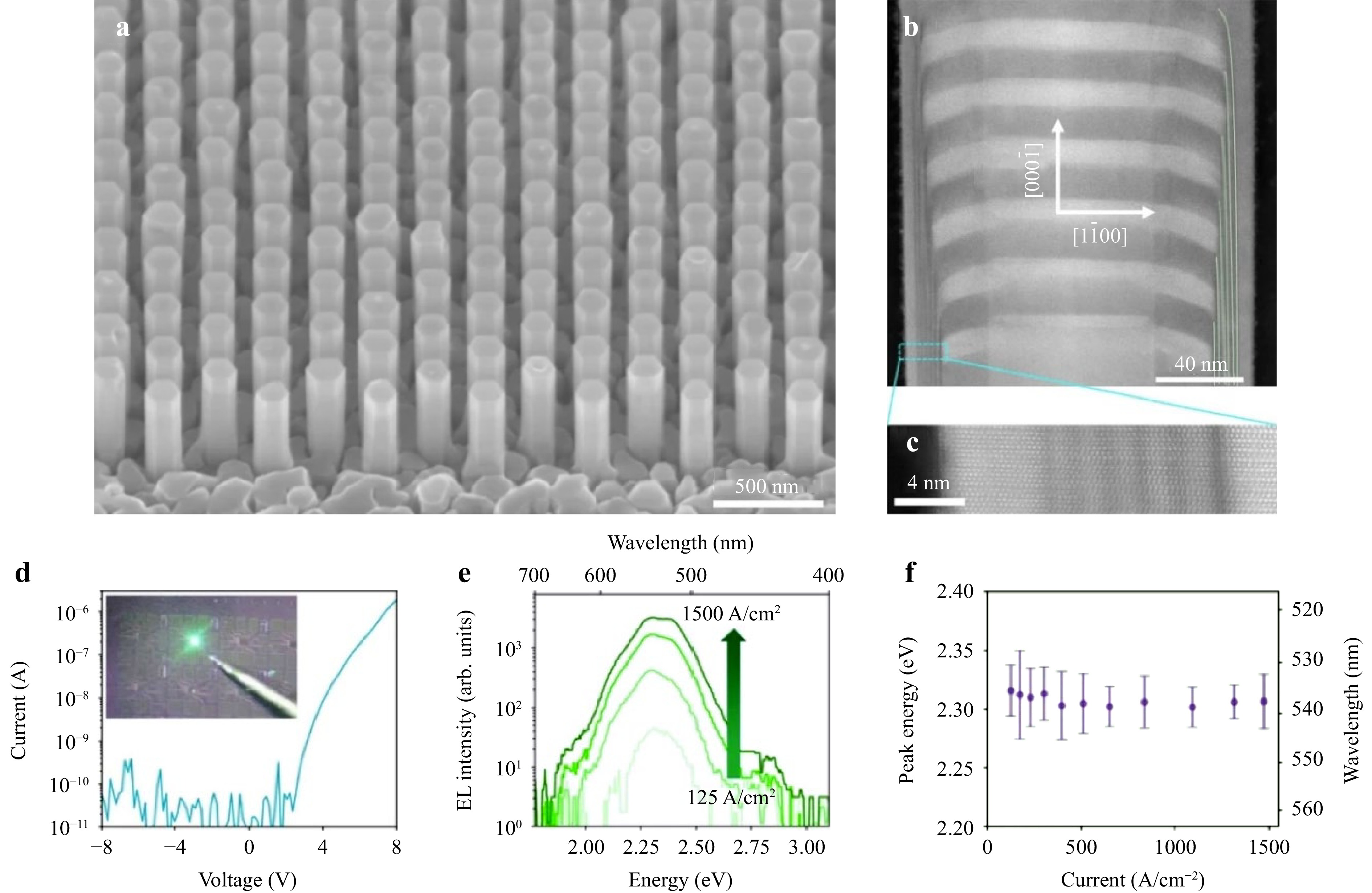
Fig. 14 a SEM image of an N-polar nanowire array grown on silicon. b HAADF-STEM image of the active region of the nanowires. The green lines show the AlGaN shell around the active region. c High-magnification HAADF image of the cyan-box region in b, showing the formation of a GaN/AlGaN superlattice on the sidewall. d J-V curve for a sub-micron scale green-emitting nanowire micro-LED. The inset shows an operating device. e Injection-dependent EL spectra of the device. f Variation of the emission peak with injection current for the device. This figure has been reproduced from the Ref. 188: Y. Wu et al., “InGaN micro-light-emitting diodes monolithically grown on Si: achieving ultra-stable operation through polarization and strain engineering”, Light: Science & Applications, vol. 11, no. 1, pp. 1-9, 2022.
As has been previously shown, the emission color of nanowires is also strongly dependent on their dimensions and spacing2, 177, 224-226. During selective area growth of InGaN by molecular beam epitaxy, the incorporation of metal adatoms depends on both the incoming metal flux, along with a contribution from the adatom migration along the lateral surfaces of the nanostructures. This is especially true for In adatoms, which have a diffusion length of ~100 nm depending on the growth temperature177, that is comparable to the dimensions of nanostructures. It should be noted that there is also a difference between the epitaxy of tightly packed nanowire arrays and single nanowires with large spacing in between them, as nanowire arrays have the added effect of shadowing of the impinging metal flux. By designing nanowires with different diameters, the nanowires will have different InGaN compositions, and hence different emission wavelengths. By exploiting this unique effect, nanowires with emission from blue to red, covering the entire visible spectrum, were grown in a single epitaxial step, using selective-area epitaxy by patterning openings of different diameters on a substrate as shown in Fig. 15a224. The nanowires of smaller diameters were observed to have a red-shifted emission wavelength. A schematic of the grown nanowires is shown in Fig. 15b with the emission color of the different nanowires indicated in the diagram, along with the heterostructure of the nanowires. An SEM image of the grown nanowires is shown in Fig. 15c. The grown nanowires were fabricated into single nanowire devices, schematically shown in Fig. 16a. Probing the devices resulted in emission peaks in the blue, green, orange, and red wavelengths, attained by reducing the diameter of the nanowires. The EL spectra for the emission of the different diameter nanowire devices are shown in Fig. 16b, spanning from ~460 nm to ~660 nm. This demonstration of multi-color devices that could together form a pixel, obtained from a single growth on a single chip, highlights the unique capabilities of the selective-area epitaxy process, which could significantly simplify the integration of nano or micro-LEDs into displays for practical applications.
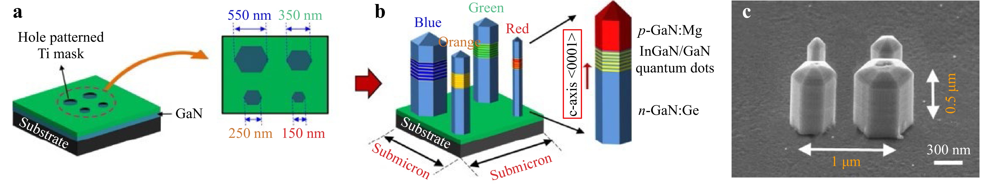
Fig. 15 a Schematic of the different size openings patterned for selective-area epitaxy. b Schematic of nanowires with different diameters having different color emission wavelengths. The different layers that comprise the nanowires are shown on the right. c SEM image of the different size nanowires that were grown. This figure has been reprinted with permission from Ref. 224: Y.-H. Ra et al., “Full-color single nanowire pixels for projection displays”, Nano Letters, vol. 16, no. 7, pp. 4608-4615, 2016. Copyright 2016 American Chemical Society.
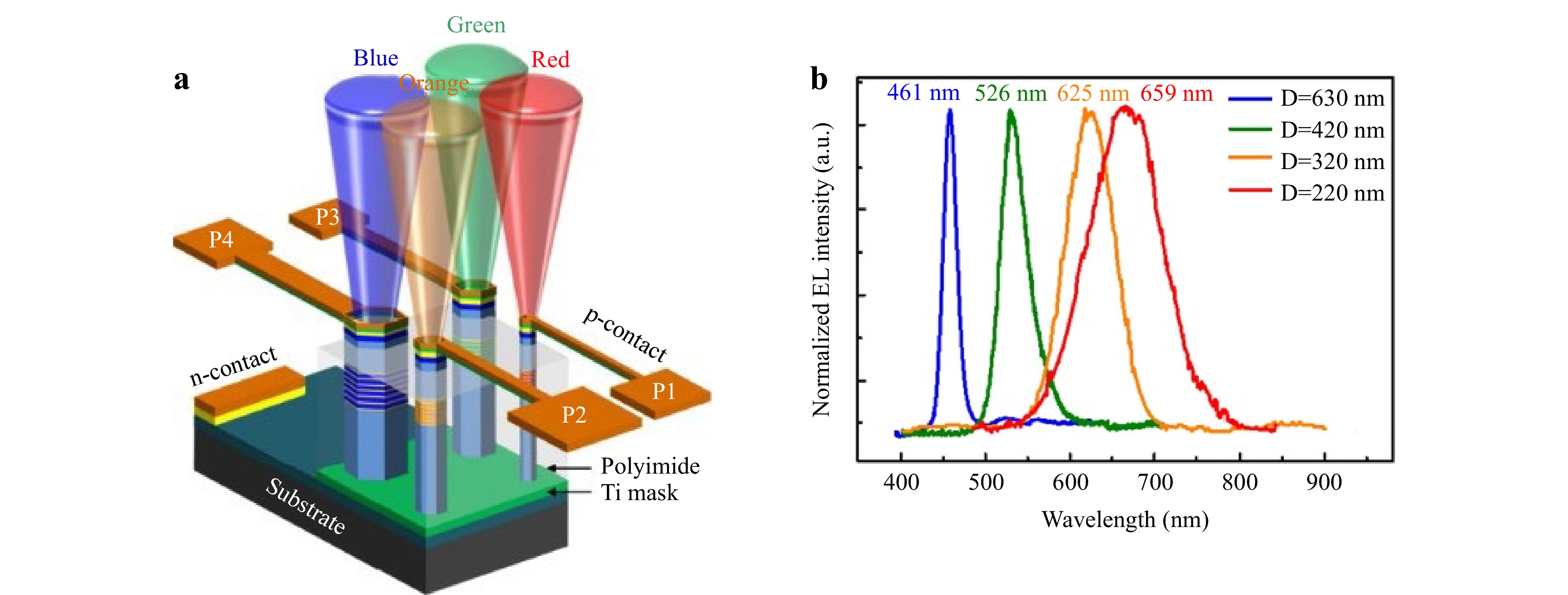
Fig. 16 a Schematic of fabricated single-wire devices having different diameters and emission wavelengths. b EL spectra of the different diameter nanowire devices. This figure has been reprinted with permission from Ref. 224: Y.-H. Ra et al., “Full-color single nanowire pixels for projection displays”, Nano Letters, vol. 16, no. 7, pp. 4608-4615, 2016. Copyright 2016 American Chemical Society.
-
From an application perspective, display technologies present the most immediate use for micro-LEDs, however micro and nanoscale optoelectronic devices will significantly impact other emerging applications as well. For example, micro-LED based optical interconnects have drawn considerable attention recently. Unlike electrical links which require high power for long distances, optical interconnects would have extremely low power consumption. The development of high-density micro-LED based optical transceivers has also enabled high bandwidths that are robust over a wide range of environmental conditions227, 228. Micro-LEDs have also attracted attention in the field of biological sensing, where they have been shown to potentially replace complicated existing sensors, as the diode of the LED can both harvest energy wirelessly (by absorbing photons) and transmit signals (by emitting photons)229. Nitride-based micro-LEDs have also been used for imaging dyes, fluorescence spectroscopy and even stimulating neurons230. Some of these unique applications may require the development of specialized micro-LED devices, that could be more easily achieved with the versatile nanostructure-based approach.
Nanostructures have shown tremendous potential to overcome critical challenges of nano or micron-scale optoelectronic devices. The difficulties in creating long-wavelength III-nitride optoelectronic devices are greatly reduced in such nanostructures, and by utilizing them as the basis of micro-LED devices, it is possible to attain efficiencies significantly greater than conventional top-down micro-LEDs, while reducing the dimensions of the devices down to the sub-micron scale. The benefits of nanostructures are further expanded through the selective-area epitaxy process. It enables the bottom-up formation of photonic crystals, that could be used to optimize the emission properties of LEDs, and even be incorporated for low-threshold, DBR-free surface-emitting lasers. The major challenge of the integration of millions of individual, multi-color micro-LED devices into a practical display can be greatly simplified through the selective-area growth approach by allowing for the growth of complete pixels in a single epitaxy step, on a variety of substrates.
These previous works have shown the promise of nanostructures and shone light on some active areas of research interest. The efficiency of green and red micro-LEDs can be improved through optimization of the p-doping in the nanowire heterostructures101. Furthermore, in the case of red-emitting micro-LEDs, research is ongoing to further improve the strain relaxation, as well as to inhibit the parasitic recombination at high currents from the SPSL layers. Nanowire micro-LEDs also typically peak in efficiency at relatively low injection currents, showing strong droop at higher injection currents. The use of an AlGaN electron blocking layer in these devices could reduce the droop effect, and also form an Al-rich shell around the active region. While a tunnel junction contact has been demonstrated for nanowires100, 231, 232, the use of such a structure in N-polar devices, grown using selective area epitaxy, is of ongoing interest as it can improve both the charge carrier injection, as well as reduce efficiency droop. Optimized devices could be used in photonic crystals to realize narrow-linewidth, spectrally pure high efficiency micro-LEDs, which could even be integrated monolithically on a single chip. Finally, as the properties of nanostructures grown using selective-area epitaxy is sensitive to their dimensions, it is critical to carefully control and fabricate the substrate before epitaxy, as well as the nanostructure devices afterwards.
In polar semiconductors such as InGaN, the distinct ionic character can lead to strong electron phonon coupling effect, which may significantly impact their electronic, optical and excitonic properties. Recent theoretical and experimental studies have revealed that the exciton binding energy in nanoscale III-nitride heterostructures can be dramatically increased, compared to their bulk structures188, 233-236. As an example, the exciton oscillator strength can be enhanced by one to two orders of magnitude in InGaN nanostructures with efficient strain relaxation235. Theoretical studies have further shown that polaronic exciton contribution to the binding energy can be as large as 190 meV in GaN nanowires237. Moreover, recent studies have shown that the strong exciton-phonon interaction, i.e., the formation of polaronic excitons, can further impact the charge carrier transport, relaxation, and recombination. For example, the unique polaronic exciton effect can transform an indirect bandgap h-BN to be extremely bright light emitters in the deep UV238. As such, we envision that a fundamental study of excitons in InGaN deep nanostructures could offer a path to break the efficiency bottleneck of micro and nanoscale LEDs.
The potential uses for micro-LED technologies have motivated considerable resources into their development. While obstacles remain in the path of nanostructure-based micro-LEDs, they can be solved by a fundamental understanding of the physics and properties of III-nitride-nanostructures and the further development and refinement of the epitaxy and fabrication methodologies. Accordingly, III-nitride nanostructures offer a very promising path to overcome the efficiency, scaling, and integration challenges of micro-LEDs for many emerging and demanding applications.
-
The contents presented in this review article are based on results published in the literature, including those at the University of Michigan. For the studies performed at the University Michigan, we acknowledge the support from NS Nanotech, Inc., U.S. Army Research Office, and National Science Foundation.
Recent progress on micro-LEDs
- Light: Advanced Manufacturing 4, Article number: (2023)
- Received: 23 February 2023
- Revised: 21 August 2023
- Accepted: 25 August 2023 Published online: 06 December 2023
doi: https://doi.org/10.37188/lam.2023.031
Abstract: With the advent of technologies such as augmented/virtual reality (AR/VR) that are moving towards displays with high efficiency, small size, and ultrahigh resolution, the development of optoelectronic devices with scales on the order of a few microns or even smaller has attracted considerable interest. In this review article we provide an overview of some of the recent developments of visible micron-scale light emitting diodes (LEDs). The major challenges of higher surface recombination for smaller size devices, the difficulty in attaining longer emission wavelengths, and the complexity of integrating individual, full color devices into a display are discussed, along with techniques developed to address them. We then present recent work on bottom-up nanostructure-based sub-micron LEDs, highlighting their unique advantages, recent developments, and promising potential. Finally, we present perspectives for future development of micro-LEDs for higher efficiencies, better color output and more efficient integration.
Research Summary
Efficient Lighting at Submicron Scales using Nanostructures
The advent of advanced displays, including for applications such as augmented/virtual reality have created a demand for efficient, small-size light emitters, which have hitherto been difficult to attain. Nanostructures can address this need, with their near-perfect crystals, as well as the freedom to arrange them in specific geometries to control their light emission. The epitaxy, and hence properties, of such structures is dependent on their size, allowing for a new and unique control over them. This makes them well-suited for the development of high-efficiency devices, and the effect of size can be harnessed to attain nanostructures with a wide variety of properties from a single step. In this work, Professor Mi’s team from the University of Michigan, USA has highlighted some recent results on nanowire-based devices to showcase their potential for creating nanoscale optoelectronic devices.
Rights and permissions
Open Access This article is licensed under a Creative Commons Attribution 4.0 International License, which permits use, sharing, adaptation, distribution and reproduction in any medium or format, as long as you give appropriate credit to the original author(s) and the source, provide a link to the Creative Commons license, and indicate if changes were made. The images or other third party material in this article are included in the article′s Creative Commons license, unless indicated otherwise in a credit line to the material. If material is not included in the article′s Creative Commons license and your intended use is not permitted by statutory regulation or exceeds the permitted use, you will need to obtain permission directly from the copyright holder. To view a copy of this license, visit http://creativecommons.org/licenses/by/4.0/.

 DownLoad: