


-
Photonic integrated circuits (PICs), which involve the dense integration of optical components and systems on planar substrates1-4, have been widely applied in communications5, ranging6, sensing7, computing8, spectroscopy9, and quantum technology10. The scalable manufacturing of PICs is now an industry norm that leverages mature semiconductor-fabrication technologies derived from electronic integrated circuit (EIC) processing to reduce costs while enhancing performance11,12.
Photonic packaging presents a different perspective. Compared with electronic packaging, the packaging of PICs demands a much higher alignment accuracy owing to the strict matching conditions for optical modes13-15. The alignment tolerance of optical interfaces is typically at the micron or even submicron level, which is one order of magnitude smaller than that of solder bump connections in electronic assemblies16-18. The tight alignment tolerance of PICs makes them incompatible with mainstream electronic packaging techniques and infrastructure, precluding cost reduction by exploiting economies of scale. Moreover, the heterogeneous or hybrid integration of multiple material platforms, such as silicon III-V, and lithium niobite, is increasingly in demand to fulfill new functionalities that Si-based materials alone cannot offer. The ability to accommodate advanced heterogeneous or hybrid integrated platforms is another obstacle in photonic packaging. New packaging technologies and device architectures are required to address these challenges19-22.
Two-photon lithography (TPL) is an emerging approach that has received significant attention in recent years23,24. TPL is a laser direct-writing technology capable of carving almost arbitrary 3-D structures with resolutions well below the classical diffraction limit24; it was first reported in 199725, and has since been adapted to form on-demand optical connections26-34. TPL offers several unique advantages for photonic packaging35.
1) In integrated photonics, light guiding can occur in various material platforms, such as silicon, glasses, III-V semiconductors, lithium niobate, and polymers, with significant differences in mode size and profile. TPL is uniquely suited for constructing broadband 3-D photonic structures with numerous geometric degrees of freedom to facilitate on-demand beam shaping and mode transformation between different waveguide systems. This is critical for achieving high coupling efficiency with wide bandwidths when connecting different optical components in a system (e.g., from lasers to single-mode waveguides).
2) TPL can be used to form optical connections between photonic components after assembly because the shape of the connections can be customized according to the relative displacement between the components. This approach significantly relaxes the alignment tolerance during PIC assembly and enables the utilization of standard electronic assembly techniques such as pick-and-place.
3) TPL can create high-channel-density, low-loss 2.5-D or 3-D links to accommodate the height differences between the optical ports inside a package. This is particularly important for hybrid integration in which modules are patterned on different substrates with varying thicknesses. This feature relaxes the accuracy and uniformity requirements during wafer lapping and deep trench etching36-38. Commonly used TPL resins exhibit broadband low optical attenuation, making them suitable for building low-loss optical links between dissimilar material platforms.
4) In addition to creating optical links, TPL can be used to form micro- and nano-mechanical structures to guide precise component placement in a passive alignment process or in pluggable optical connectors.
In this study, we present a comprehensive overview of the latest advances in TPL technology for integrated photonic packaging. Fig. 1 shows schematics highlighting these packaging methods. The basic principles of TPL are briefly introduced, followed by a survey of TPL-based photonic packaging methods. We then focus on their commercial implementation in the photonics industry and conclude by discussing of future research directions.
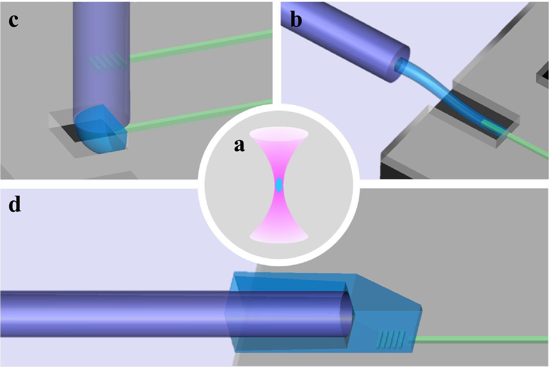
Fig. 1 Schematic drawings of three typical packaging methods based on TPL. a Illustration of a TPL voxel located at the focal spot of a laser beam. The focal spot is translated through the volume of the resin to enable direct writing of 3-D structures. b Photonic wire bond. c Freeform microoptics. d Mechanical alignment structure.
-
TPL is a 3-D printing technology that leverages a focused laser beam to selectively solidify a liquid photopolymer. The focused laser light causes two-photon polymerization (TPP) of the photoresist, leading to a solid structure. Unlike single-photon lithography, TPP occurs when the laser intensity exceeds a certain threshold value at the laser focal spot. Thus, TPL enables a more controlled and localized polymerization process, which results in finer resolution and higher precision.
A schematic of a typical TPL printing system is shown in Fig. 2. The laser, operating in the near-infrared region, is focused onto the sample by the objective lens, delivering a high light intensity that is absorbed by the photoinitiator present in the photoresist via two-photon absorption. To select a suitable magnification for the lens, the writing speed must be balanced with the desired resolution. A higher magnification yields a finer structural resolution, but results in a significantly reduced writing speed. A confocal imaging system helps locate the sample surface and enhances alignment accuracy. The galvo scanner and sample stage define distinct writing schemes, which are discussed in Section 2.3. All components are connected to a computer for remote control and programming. Before printing, the software prompts a user interface that enables the operator to input the desired 3-D model and set printing parameters such as layer thickness and laser intensity. Full automation of such printing systems endows the TPL tool with a complex and highly precise system that enables the creation of intricate, high-resolution 3-D structures for a wide range of applications.
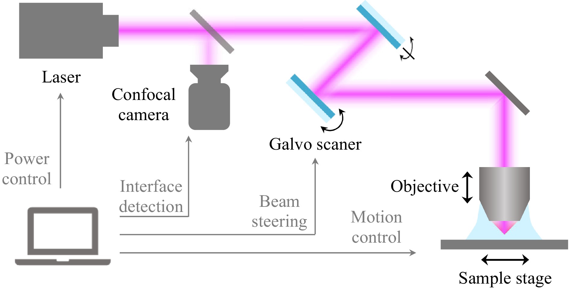
Fig. 2 Key components of a typical commercial TPL system.
-
The immense power of TPL to unlock the third dimension has enabled researchers to fabricate a variety of functional structures with exceptional performances in disparate applications, ranging from optics39-41 to biomedicine42-47. The simple operation mechanism of TPP enables a wide range of material classes to be used, which further adds to the value offered by this technique.
The most mature family of chemicals used as the basis for TPP resins is acrylates (Fig. 3a), and a variety of commercial formulations specially designed for TPP48 are already available. Polymer chains are formed through a free-radical polymerization process44 that is compatible with a variety of photoinitiators. These polymers reach extremely high printing resolutions49 and excellent optical50 and mechanical properties51,52. Some examples of resins belonging to this polymer class include the series of “IP” resists, commercially available from Nanoscribe GmbH, or “Up” resists, available from UpNano GmbH. For instance, IP-Dip, one of the most commonly used members of the IP family of resins, is a photoresist designed for TPL to achieve the highest resolution. IP-Dip’s chemical composition is approximately CH2N0.001O0.34, with the majority of the volume (60%–80%) being pentaerythritol triacrylate (PETA)48. IP-Dip is an index matched with immersion oil, for which high numerical aperture objectives are used to reduce structural distortions. This has enabled researchers to demonstrate the accurate printing of sub-100-nm features through sub-threshold resist exposure53 or controlled heat treatment-induced shrinkage54.
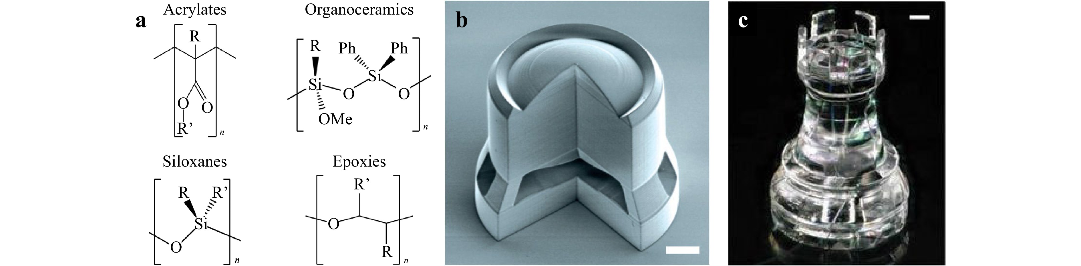
Fig. 3 Resin for TPL. a Polymeric backbone for some common TPP resins. In the chemical structure of organoceramic polymers, Me and Ph stand for methoxy and phenol groups, respectively. b Scanning electron micrograph of a doublet compound lens made of an IP-S acrylate-based photoresist. Reprinted from Gissibl et al.93. Scale bar, 20 μm. c Fused silica micro-rook fabricated through the debinding and sintering of a printed GP-Silica structure. Scale bar, 200 μm. Reprinted from Kotz, et al.74.
Other notable members of the IP family of resins include IP-n162, a resist designed for microoptics that boasts a high refractive index55, and IP-S, which features a low degree of shrinkage in tandem with a smooth surface finish56. These photoresists have been used extensively in the production of microoptical devices, including reflective elements for coupling light into an optical fiber57,58 or refractive/diffractive microlenses40, 41, 59 (Fig. 3b). UpNano’s UpBlack and Nanoscribe’s IP-Black are two more formulations of particular interest in optics, as they enable the design of novel optics where not only the path of light is controlled through transparent refractive elements but also by modulating the intensity with absorptive elements39. For instance, Schmid et al. demonstrated the benefits of combining transparent and opaque structures fabricated via TPP to form microoptical elements with vastly improved contrast, such as a pinhole camera or telecentric lens with a custom 3-D aperture, with vastly improved contrast39. Another technologically relevant photoresin is UpThermo, a resist developed in collaboration with UpNano and Cubicure for hot lithography60. The increased thermal stability of UpThermo provides an obvious advantage over other photoresins for situations in which printed structures must undergo thermal processes after printing and development. This feature makes it an intriguing alternative to backend-of-the-line solutions for electronic/photonic packaging, which requires elevated temperatures for solder reflow or eutectic bonding13.
Siloxanes are another family of resists extensively used in industry and academia. These chemicals have a polymeric backbone composed of alternating silicon and oxygen atoms (Fig. 3a) and can perform free radical or cationic polymerization48. The most prevalent photoresist belonging to this family is polydimethylsiloxane (PDMS), which is available from Nanoscribe in the form of IP-PDMS, as a formulation tailored for TPL, as well as from other vendors. This resist has been used for a range of applications in life sciences and microfluidics61,62 owing to its non-cytotoxicity, flexibility, ease of functionalization, and optical transparency63.
Another family of polymers that is relevant is epoxies (Fig. 3a), which have already become the material of choice for various applications owing to their excellent properties as adhesives64 and coatings65. Although epoxy-based formulations are not as common as acrylates in TPL because of their requirements for thermal postprocessing to achieve complete polymerization of the printed structures, their lower shrinkage66 gives them a key advantage for the printing of structures with critical size requirements. The chemical backbone of epoxies is composed of carbon and oxygen, which are formed upon cationic polymerization by opening the epoxide ring44. The most common epoxy-based TPL formulation is SU-8, which has been successfully used to fabricate high-aspect-ratio structures67, microswimmers68, and microfluidic channels69.
Finally, a wide variety of organic-inorganic hybrid polymers has been proposed as potential TPL photoresists. A famous family of these compounds is organoceramics, most famously Microresist Technology GmbH’s ORMOCERs (organic modified CERamics). Their chemical structure is composed of a Si-O polymeric backbone (Fig. 3a), with side groups determining the final properties of the polymer70. The most well-known member of the ORMOCER family is OrmoComp, a hybrid organic-inorganic photoresist with the molecular formula C21SO8SiH3648. OrmoComp has low optical absorption from infrared to near-UV55 as well as high printing resolution71 and thermal stability48, making this photoresin have potential applications in optics and related fields72.
SZ2080 is another hybrid organic-inorganic sol-gel photoresin manufactured by IESL-FORTH with the chemical formula C4H12SiZrO248, and its structure is similar to that of OrmoComp, except that the silicon atoms are substituted with zirconium atoms48. Recently, it was reported that the full conversion of SZ2080 into a completely inorganic material can be achieved by calcination of the printed structures at 1100 °C73.
A similar approach to the calcination of SZ2080 was used to demonstrate a resin capable of printing glass, Nanoscribe GP-Silica74. This photoresin is based on a methacrylate/acrylate polymeric backbone with dispersed fused silica particles of ~40 nm diameter74. This has evolved from applications in mold casting75 and later 3-D stereolithography printing76 to high-resolution and commercially available TPL resists. The printed structures can be converted into transparent glass parts through a two-step process consisting of a debinding step at 600 °C to remove the organic component (which results in a highly porous structure) and a sintering step at 1300 °C to fuse the particles together74, yielding a transparent part with optical properties comparable to those of fused silica, as shown in Fig. 3c. The structures exhibited considerable shrinkage, in excess of 25%, which could be used to produce parts smaller than the resolution limit of the printing process74.
The embedding of nanoparticles within two-photon resins to produce composite structures is not limited to fused silica; a large variety of materials have already been demonstrated. This process adds one more dimension to tune the final properties of printed structures by imparting functions that polymeric materials normally lack, for example, a large refractive index, high thermal conductivity, or high magnetic response. Suter et al.77 fabricated microswimmers that could be controlled through the application of an external magnetic field by embedding magnetite nanoparticles (~11 nm diameter) in SU-8. Masui et al.78 fabricated methyl methacrylate (MMA) structures with a dispersion of Au nanorods for application in plasmonics. Similarly, Marino et al.79 doped OrmoComp with barium titanate nanoparticles to create piezoelectric scaffolds for cell stimulation34,35.
Another family of materials that has sparked the interest of the scientific community is hydrogels, that is, materials composed of a polymeric solid network with interstitial fluids. Hydrogels have shown many promising applications in the biomedical fields and life sciences80, for example, as scaffolds for cells81. Hydrogels designed for life sciences are already commercially available; for example, BIO INX. In addition to their vast array of biological applications, hydrogels have also been used as a medium for embedding other materials82,83, enabling the fabrication of 3-D structures with novel optical properties. For instance, the inclusion of cobalt-doped titanium oxide (CTO) into hydrogels has been reported to enable the fabrication of structures with large transparency windows all the way down into the UV and tunable birefringence upon the application of a weak magnetic field, enabling the facile modulation of light with promising applications in photonic packaging, flexible optics, and broadband anisotropic optical elements82,83.
In the context of functional materials, much work has been done toward the realization of solid metallic or ceramic components through TPP to reduce the critical dimensions that can be commonly achieved through additive manufacturing82. For instance, Vyatskikh et al.46 used a custom nickel-acrylate resin to produce solid nickel parts upon pyrolysis and H2 reduction of the metal. A similar approach was adopted by Luitz et al.46, who engineered a platinum-containing organic-inorganic hybrid resin to fabricate solid metallic parts after a debinding process and full reduction of platinum salts. Other research groups84,85 used hydrogels to achieve similar results. Sol–gelFor the case of ceramics, sol-gel templates that can be preferentially polymerized using a two-photon process have been investigated for use in ceramics86.
In addition to inducing the localized polymerization of a photoresist, TPL has also been used to successfully pattern other material systems in three dimensions, most notably chalcogenide glasses87-90 and metal–organic frameworks91,92. Wong et al.88 fabricated a 3-D woodpile photonic crystal using As2S3. The chalcogenide glass was deposited at a high rate and low temperature, yielding an initial structure rich in As4S6 cages, which could then be converted back into a stable As2S3 network, enabling the selective removal of leftover material via wet etching. Similarly, Yu et al.92 identified a metal organic framework whose fluorescence could be spatially modulated by direct laser writing (as a two-photon process) or direct UV irradiation.
In conclusion, the large library of materials compatible with direct laser writing enables designers to produce structures with finely tuned 3-D geometry as well as physical properties. We predict that in the coming years, as customized resins and novel active materials will be developed, TPL will become increasingly relevant as a manufacturing technology capable of bridging the gap between macroscale additive manufacturing and 3-D high-resolution lithography.
Resin Composition n (λ = 780 nm) E (GPa) Density
(g/cm3)Viscosity at 20 °C
(mPas)Remarks IP-Dip Acrylate (PETA) 1.5455 0.75−2.594 1.17 2420 High Resolution IP-S Acrylate ~1.4950 2.1 1.11 13600 Smooth surfaces IP-Visio Acrylate ~1.5055 0.17 ± 0.1595 − − Non-cytotoxic, low fluorescence IP-n162 Acrylate ~1.6155 − − − High refractive index PDMS Siloxane, CH3NSi(CH3)3 ~1.496 ~0.015 1.01 ~100 Soft, non-cytotoxic OrmoComp Organoceramic ~1.5155 ~1 ~1 2000 Low absorption down to violet SU-8 Epoxy ~1.56 ~465 ~1.1 ~12000 Low shrinkage, well established GP-Silica SiO2 (After post-processing) ~1.4597 68.3 − − Glass part after post-processing Note: n, refractive index; λ, wavelength; E, Young's modulus. Data without marked references are quoted from the vendor. Table 1. Properties of resins for TPL.
-
In contrast to one-photon lithography, in which exposure is applied to a 2-D plane, the polymerization reaction of TPL only appears at the focal point with a high optical intensity. Thus, the voxelization of a geometry followed by point-by-point exposure is an essential procedure for the construction of 3-D photonic structures, resulting in a tradeoff between surface quality and throughput98. A finer slicing and hatching distance or higher voxel overlap benefits surface smoothness and shape accuracy, but burdens the writing speed. Conversely, a coarse mesh introduces a step effect99 and degrades the surface quality, which can exacerbate optical scattering and loss in photonic applications.
Several slicing strategies have been proposed to overcome step effects, particularly for curved surfaces98. Instead of uniform slicing and hatching (Fig. 4a), annular scanning100,101 and equal-arc scanning102 modes are two representative slicing schemes that can achieve a much smoother surface (Fig. 4b). The slicing thickness was dynamically changed by considering the slope of curvature to mitigate the surface roughness and shape error. Furthermore, a smart slicing strategy of dynamically adjusting the voxel size simultaneously (Fig. 4c) can help obtain a better fit of the curvature without increasing the number of layers. Roughness down to 14 nm was achieved on a non-spherical microstructure with planar facets and relatively sharp edges and corners, simultaneously showing 3- and 5-fold reductions in roughness and throughput, respectively103.
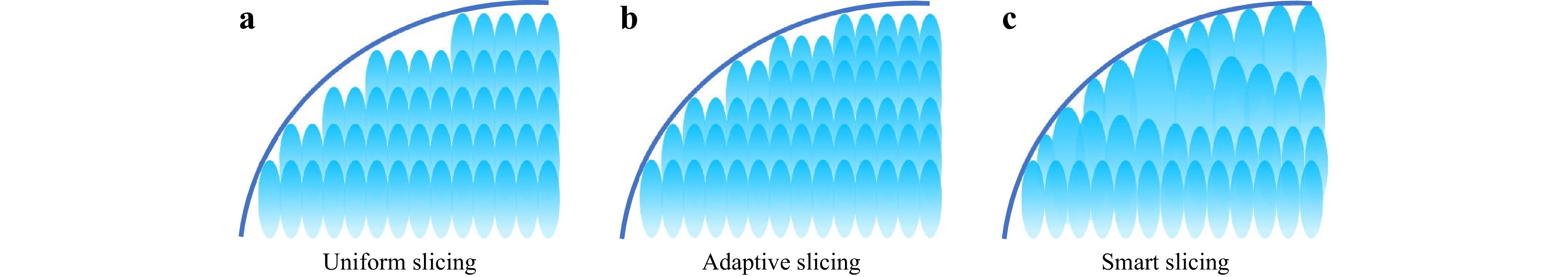
Fig. 4 Slicing strategies of TPL. a Uniform slicing with equal slicing height and hatching distance. b Adaptive slicing with changeable slicing thicknesses. c Smart slicing with dynamically changing slicing distances and voxel sizes.
In addition to the slicing scheme, there are other approaches for improving the surface quality and throughput104. Drawing upon super-resolution imaging methods, the resolution can be improved by stimulated emission depletion (STED) lithography105 and peripheral photoinhibition (PPI) lithography106. A voxel size of 36 nm can be achieved by mitigating the systematic chromatic aberration107 far beyond the diffractive limit. The profile/contour-scanning mode is another approach for mitigating roughness by tracing the outer contour profiles of structures in 3-D space108. Its combination with the flood exposure of the inner core is a promising strategy for improving both surface quality and throughput. Thermal reflow is also an efficient method for reducing the surface roughness of TPL-defined structures109.
-
The concept of photonic wire bonding was first introduced at Karlsruhe Institute of Technology in 201226. Similar to electrical wire bonding, which draws free-standing metal wires to connect metal contacts, photonic wire bonding leverages TPL technology to directly write polymer waveguide connections for optical couplings, as shown in Fig. 5a. In this scenario, multiple chips (or submodules) and fibers were placed and bonded to a carrier. The polymer waveguides were subsequently directly written using TPL to form interconnects between the optical channels on each submodule. The first photonic wire bonding (PWB) prototype consisted of two silicon-on-insulator (SOI) chips linked by SU-8 polymer waveguide connections. The PWB connections featured an average insertion loss of only 1.6 dB per bond in the C band and could transmit at an aggregate data rate of 5.25 Tbps26.
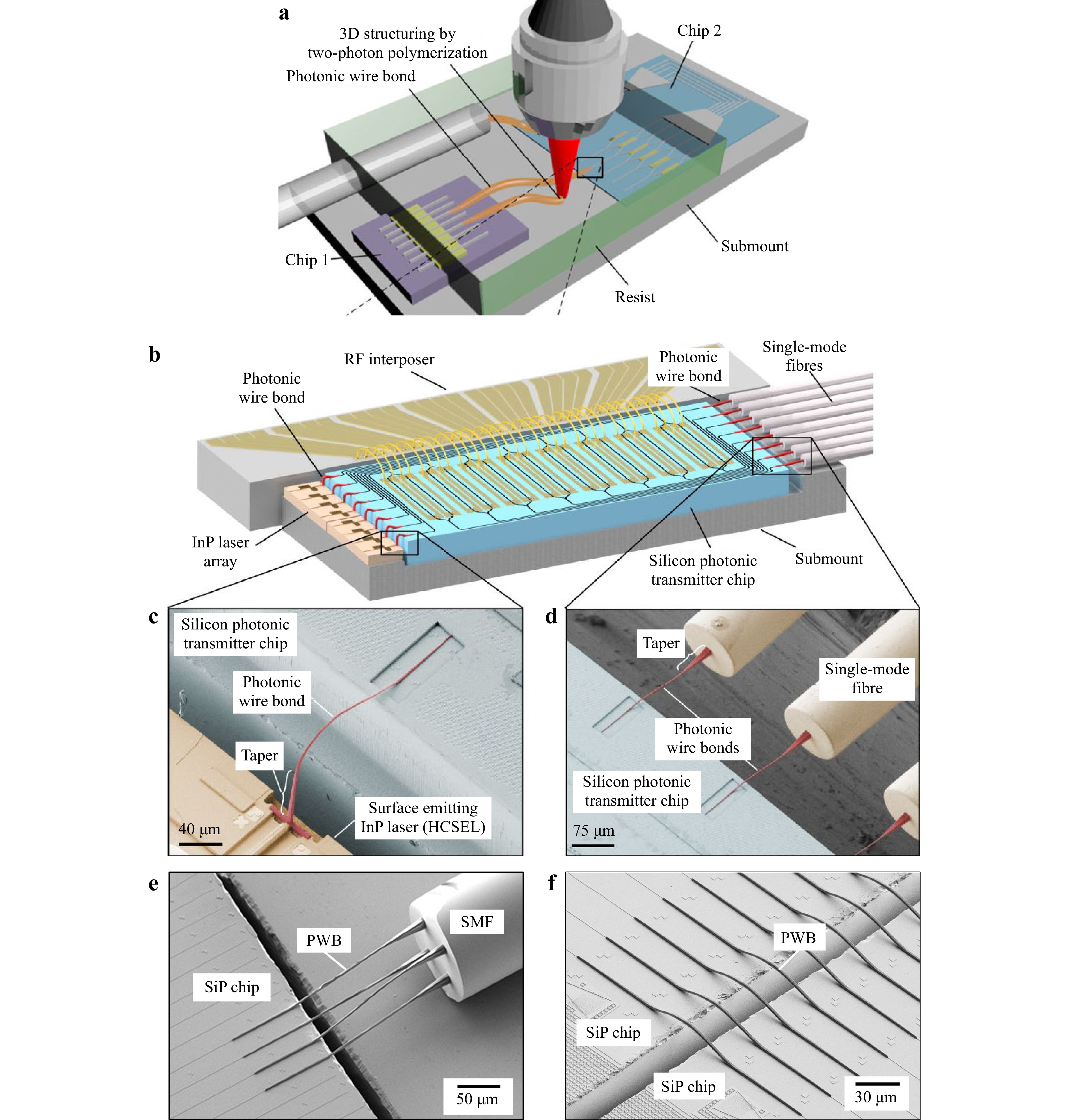
Fig. 5 Photonic wire bonding (PWB). a Schematic illustration of PWB, reprinted from Lindenmann et al.26. b−d Co-packaged hybrid multi-chip assembly module, reprinted from Blaicher et al.111. e and f Chip to multi-core fiber and chip-to-chip interconnects via PWB, respectively. Reprinted from Billah et al.110.
Over a decade of progressive development since their initial demonstration, PWB has been empowered with increased writing speed, better precision, and reduced insertion loss. This technology has also been extended to multi-chip module packaging and fiber-to-chip coupling110-114. In one example, PWB was employed to link an InP laser chip, silicon modulator chip, silicon-arrayed waveguide grating chip, and single-mode fiber, all in a single package110. Notably, PWB enables adiabatic termination with component-specific designs to be implemented on different components. For example, an InP horizontal cavity surface-emitting laser and single-mode fiber interface adopted a rectangular linear taper to match the larger mode field diameter of the laser and minimize insertion losses. A minimum PWB insertion loss of 0.4 dB was reported between the laser and silicon chips when the laser emission spot was accurately aligned with the taper. Another example is a multi-core fiber (MCF) for waveguide connections, as shown in Fig. 5e110. To minimize the insertion loss, a double-inverse taper structure was employed to match the modes between the SOI and polymer waveguides. A shape-conversion section was incorporated to adiabatically transform the square cross-section of the waveguide to a circular shape and then expanded to match the fiber mode. This design resulted in a total insertion loss of 1.7 dB. More recently, a fully packaged optical communication engine using a hybrid multi-chip assembly was reported111. Based on the same configuration, this study further co-packaged another electrical RF interposer module to simultaneously control all Mach-Zender modulators (MZMs) as indicated in Fig. 5b. The average insertion loss of PWB over 100 waveguides was 0.75 ± 0.15 dB. In addition, the robustness of such a structure to thermal cycling was tested and confirmed in 225 cycles between −40 °C and 85 °C. The photonic transmitter engine could provide a 448 Gbps aggregated data rate over a 10 km distance when bonded with eight MZMs, eight lasers, and fibers. Furthermore, coherent communication is realized by bonding a four-channel quadrature (IQ) modulator to four lasers and four fibers. An aggregate data rate of 784 Gbps over 75 km has been experimentally demonstrated. In summary, PWB is a highly versatile packaging technique for a diverse range of multi-chip platforms19,115,116.
-
Freeform optics are ideally suited for optical coupling elements owing to their capacity to sculpt light wavefronts. However, the widespread adoption of traditional bulk freeform optics has been hampered by complicated fabrication and integration procedures and high costs. Compared to simple spherical optics, freeform optics are often more sensitive to misalignment, and the resulting stringent assembly tolerance further negates the benefits of traditional bulk freeform optics. TPL presents a plausible route for producing freeform microoptics with high geometric fidelity and alignment precision. Therefore, they can be readily integrated with on-chip waveguide devices to create low-loss optical interfaces with other on-chip or off-chip components.
These freeform microoptical elements can be integrated into waveguides in two configurations. The first architecture involves the fabrication of an on-chip waveguide taper with the top cladding removed. A polymer waveguide section (typically defined by the TPL) was subsequently overlaid on top of the taper. This composite waveguide structure enables the optical mode, initially confined in the on-chip waveguide, to adiabatically transition into the polymer waveguide. The polymer waveguide then funnels light toward the freeform microoptical element, which reshapes and redirects the optical mode to match that of the other components. The advantage of this approach is that the intermediate polymer waveguide seamlessly bridges the effective index difference between high-index-contrast on-chip waveguides and polymer-based freeform microoptics to minimize reflection and scattering losses. Moreover, the small numerical aperture (NA) of the polymer waveguides reduces the beam divergence upon exit, which considerably simplifies the optical coupler design117. Fig. 6 illustrates several coupler designs based on this configuration. In all cases, light is transferred into a polymer waveguide, which either directly mates with the fiber through a 3-D out-of-plane bend or couples with a TPL-printed microoptical element to direct the light toward the fiber57,118,119. A coupling loss of 1 dB was attained in the C band using a 3-D waveguide bend coupler, as shown in Fig. 6a119. Fig. 6b shows a coupler that combines a TIR mirror and concentrating spherical lens, which achieves a coupling loss of 3.1 dB at visible wavelengths57. In contrast to grating-based approaches, these are broadband couplers; for example, operation across both the visible and near-IR telecom bands in a single coupler has been demonstrated118. A conceptually analogous design is implemented for free-space-to-surface-guided mode coupling120. Applications of these free-form couplers include photonic computing121,122, data communications123,124, optical coherence tomography125,126, quantum optics127-129, and high-power laser physics130.
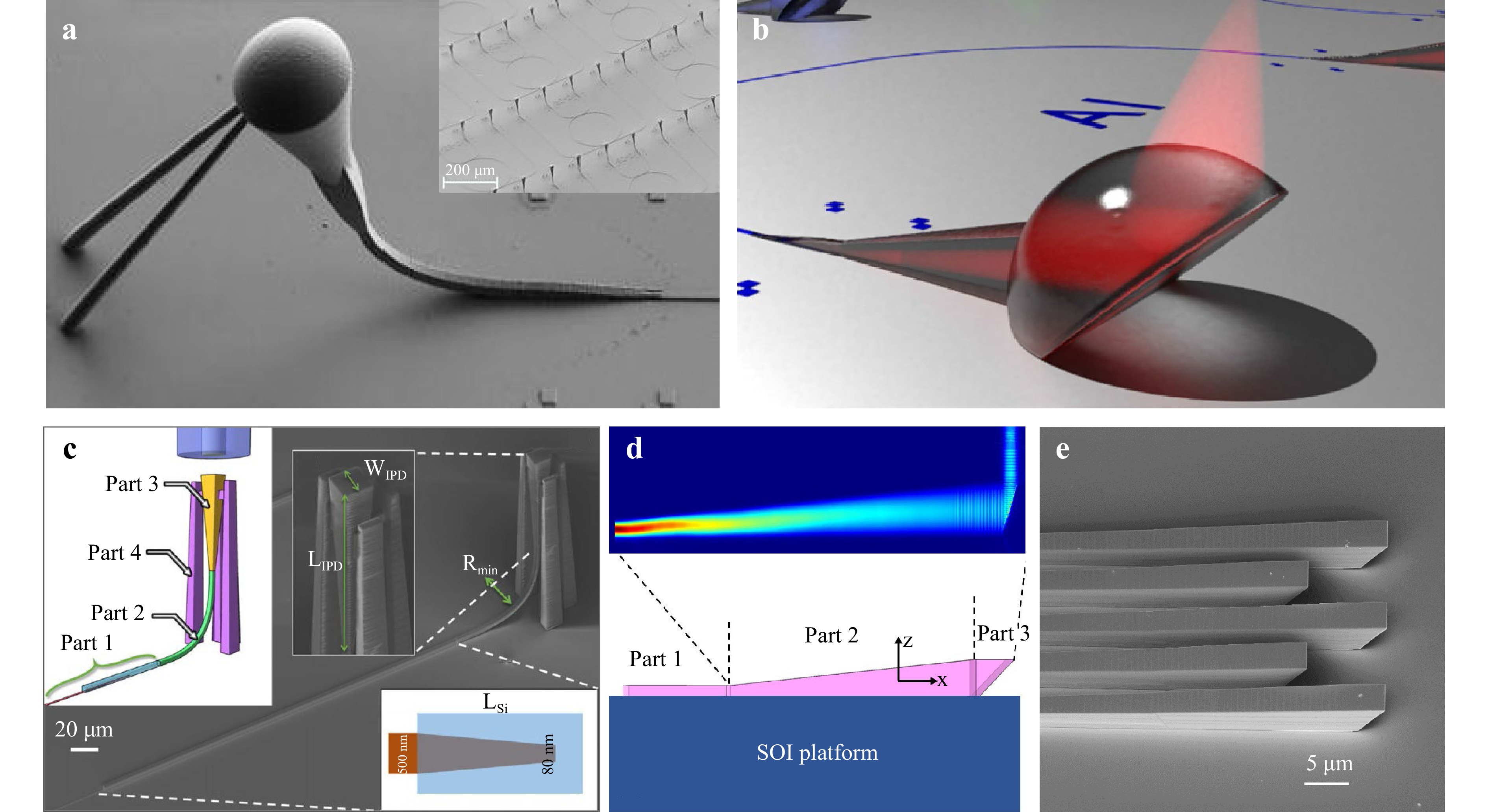
Fig. 6 Freeform microoptical couplers with a polymer waveguide-transition section. a SEM image of a waveguide to a fiber coupler.; inset: coupler array enabling high-density integration118. b Artistic view of a waveguide top attached TIR mirror. Reprinted from Gehring, H. et al.57. c Schematic drawing and corresponding SEM image of a waveguide-to-fiber vertical coupler, where a bent polymer waveguide directs the light toward a surface-normal propagation direction. Reprinted from Li, Y. et al.50. d Structure and FDTD simulation result of a waveguide-to-fiber TIR coupler; and e the SEM image arrays of the coupler. Here the TIR reflectors at the end of the polymer waveguides reflect the light upward toward the fiber. Reprinted from Luo et al.131.
An alternative configuration bypasses the cladding-removal step and directly integrates microoptics on the facet of the waveguide132. Because the backend-cladding stripping process is typically offered only as a custom add-on in photonic foundries, this configuration facilitates wafer-scale integration with standard foundry-processed PICs with minimal customization (the waveguide facets can be defined in a deep-trench etching step as part of the foundry process rather than during dicing). The avoidance of exposed waveguide cores also improves the ruggedness of the devices. Dietrich et al. demonstrated a wide variety of facet-attached microoptical beam-shaping elements for hybrid photonic multi-chip packaging41. The realized components ranged from single concentrating lenses and total internal reflective (TIR) mirrors to compound multi-lens assemblies (Fig. 7a), and their superior performance was validated. The concentrating lens/TIR mirror surfaces adopted a rotational/square symmetric polynomial of the eighth order, whose parameters were then optimized to achieve maximum coupling efficiency. The laser-to-fiber coupling loss using single free-form lenses was reduced to 0.6 dB, whereas the coupling loss from a vertical-cavity surface-emitting laser (VCSEL) to a TIR-mirror-integrated fiber was only 1.1 dB. The edge-emitting laser–chip-coupling loss was 2.5 dB with a 1-dB alignment tolerance of ± 2.5 μm. The repeatability of the TPL fabrication of these microoptical elements was also investigated with a device-to-device coupling loss variation of only 0.1 dB. These facet-attached microoptics are also applicable to the packaging of transceiver assemblies133, Kerr comb sources134,135, and lithium niobate on insulator modulators135. An interesting derivative of this concept is the printing of microoptics on the facets of a fiber array, which can be used as an optical probe for the wafer-level testing of edge-coupled devices that are normally only amenable to die-level characterization136.
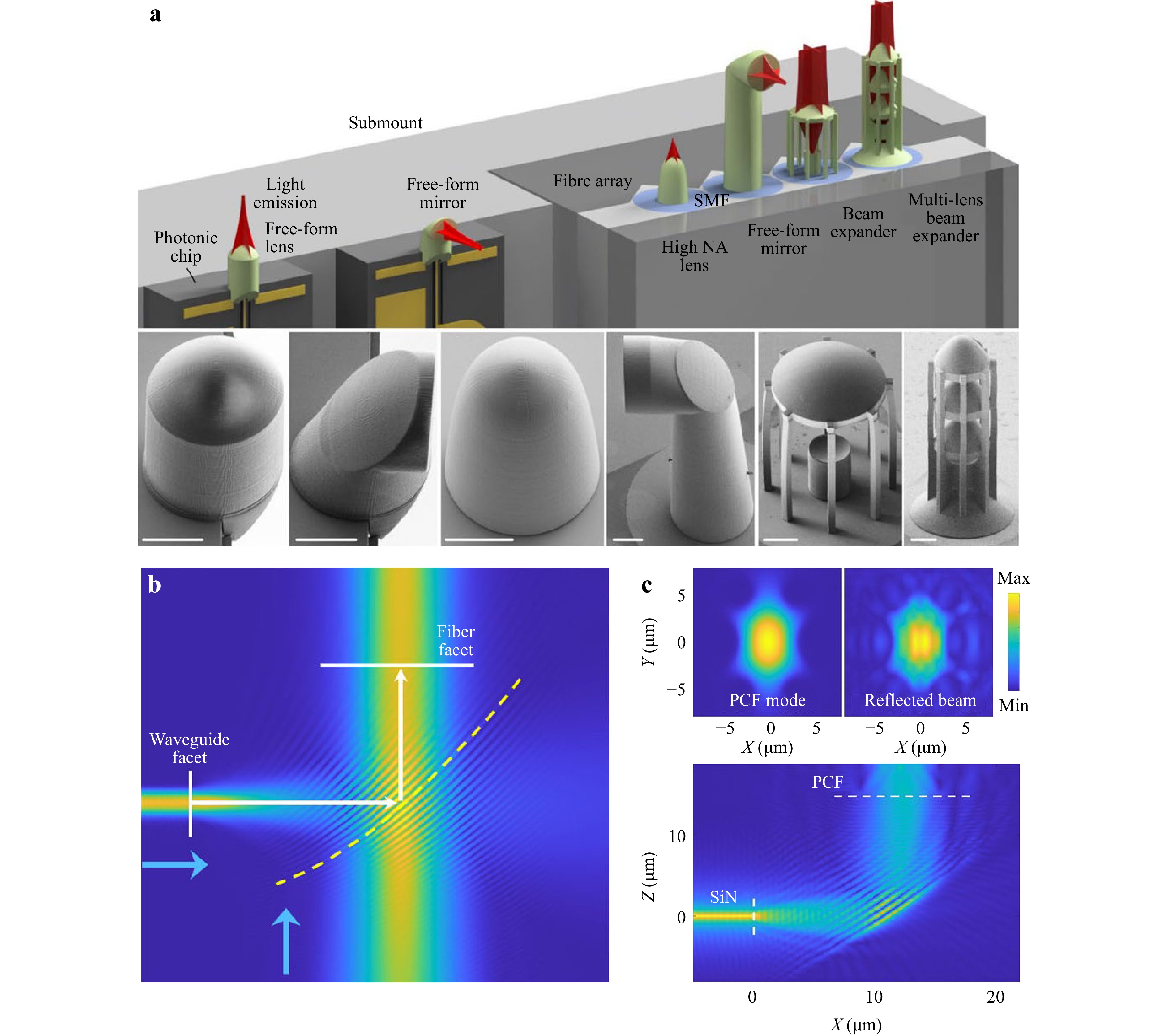
Fig. 7 Freeform facet-attached microoptics and their design methodology. a TPL-printed microoptic components for packaging, including freeform lenses, mirrors, and beam expanders. All scale bars are 20 μm. Adapted from Dietrich et al.41. b One-step deterministic design of freeform microoptics via a wavefront-based method. c Light coupling from a SiN waveguide into a photonic crystal fiber (PCF) via a facet-attached free-form coupler. b and c are adapted from Yu et al.137.
Yu et al. proposed microoptical reflectors as a ‘universal’ optical coupling platform, which they termed ‘Optical Free-Form Couplers for High-density Integrated Photonics (OFFCHIP)137. Their designs employed free-form TIR mirrors to redirect and reshape optical waveguide modes to achieve low-loss, broadband surface-normal coupling58,137. Notably, they devised a novel approach that simplified the design of free-form elements from an otherwise iterative multi-parameter search-optimization process to a deterministic method involving only two full-wave simulations. The approach is illustrated in Fig. 7b, where a forward-propagating beam from the chip and a backward-propagating beam from the fiber create interference fringes in their overlapping region. Yu et al. demonstrated that these fringes represent loci of points satisfying the Fermat’s principle, achieving a constant optical path length connecting the fiber and waveguide modes, which also yielded the optimal shape of the TIR reflector. Using this approach, the OFFCHIP platform can also be applied to coupling of light into devices with unconventional mode structures, such as photonic crystal fibers (Fig. 7c). The so-designed coupler58 features a low insertion loss of 0.5 dB at 1550 nm wavelength and an ultra-broadband > 300 nm 1-dB bandwidth for coupling from a SiN waveguide to a single-mode fiber, with in-plane and out-of-plane 1-dB alignment tolerances of ± 2.2 and 20 μm, respectively. The OFFCHIP platform can also be adapted to coupling from chip-to-chip, chip-to-interposer, and chip-to-free space with tailored beam profiles137.
-
In addition to optical coupler printing, high spatial resolution and alignment accuracy qualify TPL as a versatile solution for the fabrication of micromechanical fixtures to assist in the passive alignment of optical components during packaging138. Wan et al. introduced the fiber-interconnect Si chip technology (FISCT) for fiber-to-chip packaging139. As depicted in Fig. 8a, it employs a carrier wafer with partial and through-etched pits to connect the fibers and silicon photonic chip. The partially etched pits are intended for self-alignment with the silicon host chip, whereas the through-holes are used for the bonding of 3-D printed fiber ferrules separately fabricated via TPL. During assembly, the carrier bonded with the ferrules was first placed on the photonic chip. The fibers were then inserted into these ferrules to complete the packaging. The fibers were self-aligned to the grating coupler, aided by a thermally reflowed photoresist dome structure on a photonic chip. Submicron placement accuracy was achieved using this method140.
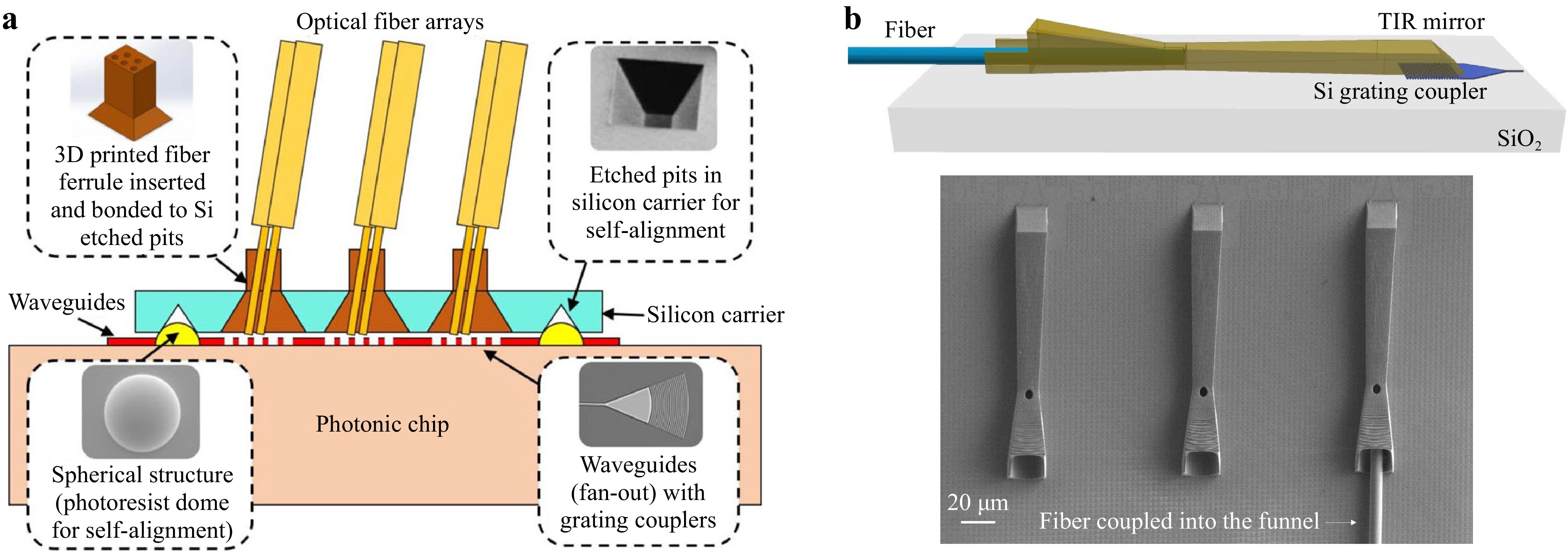
In another example, Gordillo et al. proposed a plug-and-play fiber-to-chip funnel-shaped connector module fabricated using TPL141. This consisted of a 20 μm aperture that was gradually reduced to 10 μm diameter to mechanically guide the fiber to align with the coupler center. Subsequently, the funnel was transformed into a solid-core polymer waveguide designed to match the fiber mode. Finally, the light was redirected via a TIR facet to impinge the normal surface onto a grating coupler. A schematic of this structure is shown in Fig. 8b. This coupler yielded an excess loss (relative to the coupling loss of the grating coupler) of only 0.05 dB at telecommunication wavelengths. TPL-fabricated connectors offer a reliable and robust assembly method for fiber-to-chip coupling. Although the bandwidth and total coupling loss were limited by the grating coupler in this study, combining these structures with low-loss broadband couplers will significantly improve the optical performance.
-
The industrialization of a TPL places more stringent requirements on its performance metrics. Several examples are:
1) Scalability and reliability: The first rigor of the industrial adoption of TP is its ability to consistently and reliably produce high-quality 3D structures, even when used for large-scale manufacturing.
2) Speed and precision: The cost of TPL-defined components scales directly with the printing time, among other factors. Therefore, it is essential for TPL to print structures quickly without sacrificing quality. High levels of precision and accuracy, down to the submicron scale, are required for complex 3-D structures, particularly in optical applications.
3) Ease of use: Industrialization also requires TPL tools to be easy to use and maintain. The tool should have a user-friendly interface and minimal maintenance requirements to reduce downtime and increase productivity.
Over the two decades since its initial debut, the effectivity of TPL has been validated, and several companies have already offered commercial off-the-shelf tools for TPL fabrication. Nanoscribe GmbH & Co. KG was the first to successfully commercialize TPL-based 3-D printing systems. Its latest product, Quantum X, uses a 250 mW, 780 nm femtosecond laser as the light source and offers up to 4096 level grayscale lithography capability to reduce the surface roughness to < 5 nm. The minimum feature size was 100 nm, determined using the focal spot size of the laser. The writer head scanner supports scan speeds up to 1.25 m/s when used in conjunction with a 5x magnification objective lens. The system specifies a 3-D alignment accuracy of less than 100 nm in-plane and 500 nm out-of-plane; the latter is achieved using the co-focal detection of markers. Heidelberg Instruments Mikrotechnik GmbH, in collaboration with Multiphoton Optics GmbH, launched MPO100 TPL system. The MPO100 tool is equipped with a 522 nm laser, which considerably expands the applicability of TPL polymers. Using a galvanoscanner, the tool can also scan at speeds up to 1 m/s with a 10x objective. The minimum feature size and surface roughness were specified as 100 and 10 nm, respectively. A unique feature of MPO100 is its stitching-free writing capability, which leverages simultaneous laser scanning and sample-stage movement. Compared to field-to-field writing, this continuous printing mode avoids possible discontinuities between fields. This is particularly useful for fabricating large connected structures with sizes bigger than those of a single writing field. UpNano GmbH is another company that focuses on TPL systems that feature high-power laser heads and large working distances. Their NanoOne 1000 model adopted a 780 nm and 90 fs pulse laser with an average power exceeding 1000 mW. The high power reduces the dwell time during writing, yielding a faster scan speed. In addition, it provides a vat mode for immersion lithography, where a vat with a specialty glass window protects the objective from the photoresist. Using the vat mode, NanoOne 1000 can fabricate structures up to 40 mm in height. Other companies offering TPL tools include Microlight3D, Laser NanoFab GmbH, and Innofocus Photonics Technology Pty., Ltd.
In addition to the aforementioned general-purpose TPL systems, Vanguard Automation GmbH has developed highly automated TPL tools that target photonic packaging applications. In addition to TPL printing, these systems can also performing automated dispensing of photoresist, development of exposed structures, and feature automated interface-detection functions using state-of-the-art machine vision tools.
Company Website Tool vendor Nanoscribe GmbH & Co. KG www.nanoscribe.com Vanguard Automation GmbH www.vanguard-automation.com Multiphoton Optics GmbH www.multiphoton.de Microlight3D www.microlight3d.com UpNano GmbH www.upnano.at Laser nanoFab GmbH www.lasernanofab.com Innofocus Photonics Technology Pty Ltd www.innofocus.com.au Photonic packaging service provider Dream Photonics Inc. www.dreamphotonics.com PHIX Photonics Assembly www.phix.com Table 2. TPL tool and photonic packaging service vendors
Several companies and packaging houses, such as Vanguard Automation GmbH (Germany), Dream Photonics (Canada), and PhiX (Netherlands), offer custom TPL fabrication services. For PWB in a multi-chip assembly, predefined alignment markers must be patterned near the waveguide ends to be connected by PWB. The chips are mounted side-by-side on a carrier module with the waveguide ends facing each other. Subsequently, PWB can be used to connect the waveguides on the two chips. Mounts with V-grooves are employed for the fiber-to-chip PWB service. In addition to PWB, fabrication services for facet-attached microoptical lenses or reflectors based on customer-furnished designs are available.
-
Although the latest advances discussed in this review have firmly positioned TPL as a high-performance and versatile solution for photonic packaging, innovations in several areas are warranted before TPL can become a mainstream packaging technology, as outlined below.
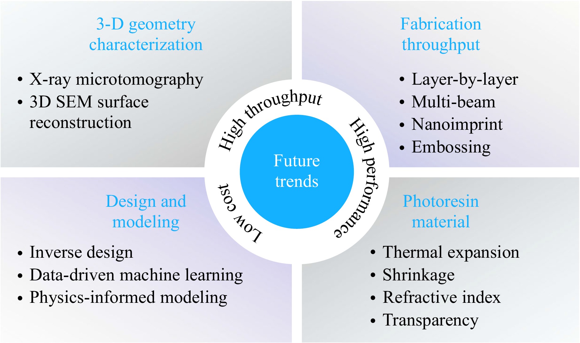
Fig. 9 Future trends for-TPL based photonic packaging.
-
High throughput is the linchpin for cost-effective volume production. The classical point-to-point TPL exposure scheme is time consuming and cannot compete with traditional packaging techniques. For example, each photonic wire bond requires tens or even hundreds of seconds to fabricate. In comparison, ~ 0.1 s per bond is typical for electrical wire bonding, which is generally not considered a high-throughput packaging technique. Several new writing schemes have been proposed to enhance the TPL throughput. The shell-and-scaffold writing scheme, with fine carving of only the shell, followed by fast coarse exposure of the core, considerably enhances the throughput of the TPL while maintaining the high-resolution advantage142. Projection-based light sheet exposure can be used to pattern complex structures layer-by-layer (Fig. 10b) instead of point-by-point (Fig. 10a), which can improve the TPL throughput by up to three orders of magnitude143,144. Multiple-beam parallel writing is another promising approach (Fig. 10c)145-147. For instance, nine beamlets generated from a diffractive optical element can be used for the parallel fabrication of large periodic arrays with submicron feature sizes145. An alternative solution to the throughput bottleneck is nanoimprinting or embossing for structure replication using TPL-fabricated masters as molds117,118.
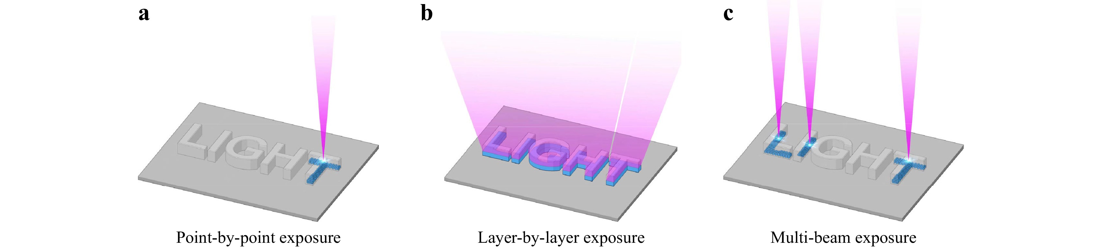
Fig. 10 Exposure strategies for improving TPL throughput. a The classical point-by-point exposure scheme. b Layer-by-layer exposure. c Multi-beam exposure.
-
Photonic packaging applications require photoresins with improved thermo-mechanical properties and shape fidelity. First, polymers still pose challenges in terms of reliability and compatibility with photonic packages. Compared with the semiconductor and inorganic dielectric materials routinely used in PICs, many polymers are more susceptible to chemical degradation owing to thermal cycling, damp heat, or UV irradiation. Polymers typically have large thermal expansion coefficients (CTEs), compared to inorganic materials, which can cause mechanical failures such as delamination. 3-D structures made entirely of inorganic materials can be printed using hybrid organic-inorganic photoresins, followed by calcination (Section 2.1); however, the calcination step often requires high temperatures that exceed the packaging thermal budget and induces large shape distortions. Second, polymer-based photoresins typically exhibit 3%–5% volume shrinkage during cross-linking, which results in inevitable shape distortion. Although such distortions can be iteratively corrected or compensated using predictive techniques (discussed later), reduced shrinkage can significantly simplify the optimization process and shorten the design cycle. Finally, photoresins with a wide refractive-index range can significantly expand the accessible degrees of freedom for photonic designs. Doping with high-index nanoparticles is one method to increase the refractive index of resins. Shifting to photopolymer chemistries containing heavier elements such as sulfur may be another approach for extending the refractive index range148.
-
Because of the vast geometric degrees of freedom made available by the TPL technique, the design of these complex 3-D micro-structures presents another challenge. We also note that, unlike conventional freeform optics, which are customarily optimized with ray tracing, microoptical elements printed with TPL represent a unique length-scale regime in which ray optics meet wave optics. Therefore, novel design methods capable of handling large parameter sets of freeform microoptics in a computationally efficient manner, while accounting for the wave nature of light, are essential. The wavefront-based design approach outlined in Section 3.2 serves as an example. Coupling emerging inverse design and optimization algorithms with TPL fabrication of complex 3-D structures is another exciting area for future investigation149.
Modeling the TPL process, which helps inform process optimization and enhances the shape fidelity of printed structures, is another important research frontier. Such models can be built on deterministic multiphysics simulations, such as the modeling of temperature and stress distribution during TPL fabrication or subsequent packaging processes150. When handling complex scenarios in which direct simulations prove difficult, data-driven machine learning is a complementary tool. Examples of its implementation include improving the geometric compliance of TPL-printed structures151, enabling automated structural quality quantification151, and developing predictive models for the constitutive relations of resin materials150. Harnessing physics-informed models may provide further insights into machine-learning techniques and expand their application to TPL process design and quality control.
-
The accurate and high-throughput characterizing of 3-D structure geometries is an important yet unresolved challenge for TPL-based photonic device fabrication. Conventional characterization methods for bulk freeform surfaces, such as white-light interferometry, are poorly adapted to microscale structures. Microscale surface metrology techniques such as profilometry or atomic force microscopy (AFM) are not applicable to surfaces with steep slopes or structures that are not fabricated on a planar substrate (e.g., facet-attached microoptics). Scanning electron microscopy (SEM) aided by an automated 3-D geometry reconstruction algorithm offers a potential solution for the high-throughput characterization of TPL-fabricated structures. Other advanced 3-D metrology characterization methods, exemplified by X-ray microtomography152, are also of significant interest for this purpose.
-
Owing to its capability for high-resolution on-demand 3-D structure fabrication and precise placement, TPL is a promising solution for alleviating the photonic packaging bottleneck. TPL has been used to demonstrate optical coupling interfaces with exceptionally low optical loss, broadband operation, and enhanced alignment tolerance. 3-D printing of micromechanical self-alignment structures to aid in facile photonic assembly is another area in which TPL can play a pivotal role. As the community witnessed the increasing adoption of TPL by the photonics industry, we foresee that this trend will be expedited with further research and development efforts to boost TPL fabrication throughput while expanding the material repertoire as well as the design and characterization toolbox.
-
S. Y. and Q. D. acknowledge funding support from the National Key R&D Program of China 2021ZD0109904 and the Key Research Project of Zhejiang Lab No. 2022PH0AC03. C. R. M. acknowledges the funding support provided by the Fulbright Program.
Two-photon lithography for integrated photonic packaging
-
Shaoliang Yu1, *, ,
 ,
, - Qingyang Du1, *, ,
- Cleber Renato Mendonca2, 3,
- Luigi Ranno2,
- Tian Gu2, 4,
-
Juejun Hu2, 4,
- Light: Advanced Manufacturing 4, Article number: (2023)
- Received: 01 March 2023
- Revised: 29 August 2023
- Accepted: 31 August 2023 Published online: 01 November 2023
doi: https://doi.org/10.37188/lam.2023.032
Abstract: Photonic integrated circuits (PICs) have long been considered as disruptive platforms that revolutionize optics. Building on the mature industrial foundry infrastructure for electronic integrated circuit fabrication, the manufacturing of PICs has made remarkable progress. However, the packaging of PICs has often become a major barrier impeding their scalable deployment owing to their tight optical alignment tolerance, and hence, the requirement for specialty packaging instruments. Two-photon lithography (TPL), a laser direct-write three-dimensional (3-D) patterning technique with deep subwavelength resolution, has emerged as a promising solution for integrated photonics packaging. This study provides an overview of the technology, emphasizing the latest advances in TPL-enabled packaging schemes and their prospects for adoption in the mainstream photonic industry.
Research Summary
Two-photon Lithography: an enabling technology for photonic packaging
With the ever growing demands on operation bandwidth and energy efficiency, optical input/output (I/O) are replacing traditional electronic copper wires with photonic interconnectors. However, its packaging still faces challenges owing to its unique requirements on optical mode matching as well as submicron alignment tolerance. Shaoliang Yu and colleagues from Zhejiang Laboratory and Massachusetts Institute of Technology review the state-of-the-art and present a summary on current integrated photonic chip packaging enabled by two-photon lithography. In addition to introducing the printing systems, writing schemes, and TPL resin materials, TPL enabled packaging technology such as photonic wire bond, free form optical couplers, as well as mechanical alignment structures are discussed in details. Industry adoption, future research and develop directions are further recommended.
Rights and permissions
Open Access This article is licensed under a Creative Commons Attribution 4.0 International License, which permits use, sharing, adaptation, distribution and reproduction in any medium or format, as long as you give appropriate credit to the original author(s) and the source, provide a link to the Creative Commons license, and indicate if changes were made. The images or other third party material in this article are included in the article′s Creative Commons license, unless indicated otherwise in a credit line to the material. If material is not included in the article′s Creative Commons license and your intended use is not permitted by statutory regulation or exceeds the permitted use, you will need to obtain permission directly from the copyright holder. To view a copy of this license, visit http://creativecommons.org/licenses/by/4.0/.

 DownLoad: