


-
An Optical Phased Array (OPA) is a nonmechanical beam-steering control device with high directivity and deflection efficiency. Owing to its high resolution, fast response, and absence of inertia1−3, the OPA is widely applied in LiDAR4−6, free-space optical communication7−9, multi-beamforming10−12 and many other fields.
Limited by the manufacturing level, the accumulation of structural errors grades the quality of the deflection beam13,14. In addition, the random phase noise induced by fabrication factors results in angular deviation and low energy efficiency.
To improve the OPA’s performance in beam steering, focusing, and energy efficiency, research has been performed to optimise the far-field distribution depending on the real-time wavefront of the deflected beam15,16. The phase distribution of the wavefront is acquired using a phase sensor or phase recovery algorithm, with which phase compensation is performed. However, it is difficult to construct a complicated system for optical path adjustment and light field acquisition. In addition, the recovery algorithm represented by the Gerchberg−Saxton (GS) algorithm17 involves a Fourier complex transform, leading to low computational efficiency.
Recently, phase-calibration approaches based on adaptive optics have been the focus of OPA-related investigation18,19. This type of approach no longer requires phase detection and reconstruction of the wavefront and directly optimises the voltage of each element to obtain the optimal beam deflection efficiency. Such adaptive optimisation approaches include simulated annealing algorithm20,21, genetic algorithm22−24, and rapid search algorithm25 and have simple experimental setup and calculation. The commonly used approach applies the Stochastic Parallel Gradient Descent (SPGD) algorithm26−28 to optimise the wavefront’s shape, which improves the performance of multi-channel processing and reduces the constraints on the objective function. However, when the number of array elements increases, the optimisation can be easily trapped at a local minimum owing to the non-convex nature of the optimisation, and the convergence speed of the evaluation function decreases significantly.
To address this problem, we propose an alternative approach for performing rapid and accurate beam deflection of the OPA. This approach conducts phase calibration individually for each array element using carefully designed mechanics. Subsequently, based on this method, the far-field diffraction efficiency of the OPA steadily increases, and the theoretical limit is obtained linearly and deterministically. Consequently, the results of numerical simulations and experiments demonstrate that, compared to a typical SPGD algorithm29, the proposed pointwise optimisation approach increases the convergence rate by 53.5% while decreasing the time consumption by 9.7%. This indicates that the pointwise optimisation approach combines the characteristics of global search and accurate calibration in different parts of the calculation process, thus reducing the number of iterations and improving the convergence speed.
-
The OPA controlled the phase of the beam emitted by each array element to control the overall deflection of the array beam. The far-field intensity distribution of a one-dimensional OPA is expressed as Equation 1, where
$\theta $ is the diffraction angle;$E(\theta )$ is the complex amplitude distribution expression, and${I_0}$ is a constant that represents the light intensity generated by all elements.$$ I(\theta ) = {\left| {E(\theta )} \right|^2} = {I_0}{\left( {\frac{{\sin \alpha }}{\alpha }} \right)^2}{\left( {\frac{{\sin N\beta }}{{\sin \beta }}} \right)^2} $$ (1) $$ \beta = \frac{{\left( {\varphi - \Delta \varphi } \right)}}{2} $$ (2) In Eq. 1, the diffraction factor,
$\alpha $ , relating to an array element width, determines the envelope of the intensity distribution. However, emphasis is often placed on the interference factor,$\,\beta $ , which determines the coherent properties of the light intensity distribution. In the interference factor$\,\beta $ ,$\varphi $ is the phase difference due to the interval between adjacent elements, and$\Delta \varphi $ is an additional phase shift, often modulated to control beam steering.The internal modulation material of the optical phase array considered in this study was LiNbO3. With a modulated electric field applied with voltage-controlled electrodes, the electro-optic effect of LiNbO3 modifies the refractive index change obtained by the optical wave, thus inducing a phase shift
$\Delta \varphi $ and realising beam deflection. Fig. 1 shows the beam steering control model.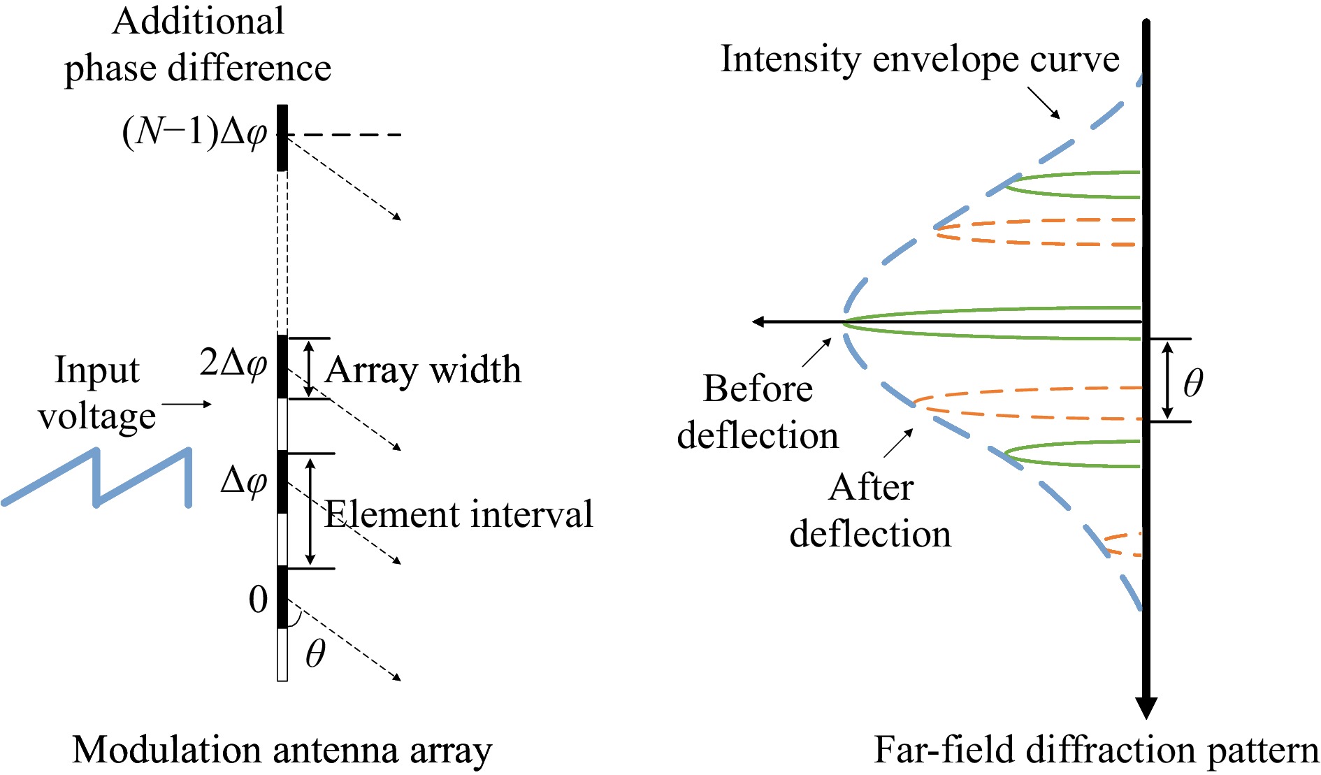
Fig. 1 OPA beam-steering controlling model. The phase shift caused by the electric field is proportional to the applied voltage; thus, different far-field distributions can be obtained.
We changed the phase-shift
$\Delta \varphi $ between array elements based on electro-optical modulation to control the far-field diffraction pattern. However, the fabrication factor causes random phase noise in optical waveguides. The existence of an unknown initial phase leads to an inability to precisely control beam deflection. Therefore, to realise precise steering of the OPA’s far-field beam, it is necessary to calibrate the initial phase. -
The initial phase degrades the quality of the output beam in terms of focusing and energy efficiency. To eliminate the effect of the initial phase, some adaptive optical approaches apply the SPGD algorithm to determine the best voltage input. Random perturbations are applied to all variables to measure the gradient estimates and iteratively search in the gradient descent direction. When the maximum value of the objective function is acquired, the calibration of the input voltage is completed.
However, the SPGD relies on the initial voltage and is often trapped in a local optimal solution. To solve this problem, the proposed pointwise optimisation approach is a global deterministic approach. It comprises two stages in the calibration process. In the first stage, the input voltage traverses the range of the 2π modulation phase and is updated when a higher diffraction efficiency is achieved. Then, in the latter stage, this approach searches based on the previous voltage until the optimum result is achieved. With the characteristics of global search in the former stage and accurate calibration in the latter stage, the pointwise optimisation approach achieves the best input voltage in each element. It thus eliminates the adverse effects of the initial phases.
The detailed process involves the following steps.
Step 1:
$ V = [{V^1}, ..., {V^k}, ..., {V^N}] $ denotes the voltage vector for an OPA with 1×N array elements, where k denotes the element to be calibrated. The step size for the different stages of the input voltage is$\delta V = [\delta {V^1}, \delta {V^2}]$ .$\delta {V^1}$ is larger than$\delta {V^2}$ . i is the current iteration time for the former stage with iteration times t1 and j for the latter stage with iteration times t2. t1 is defined as${{{V_{2\pi }}}}/{{\delta {V^1}}}$ , where${V_{2\pi }}$ denotes the voltage of the 2π phase change in the LiNbO3 modulator. t2 is defined as${{\delta {V^1}}}/{{\delta {V^2}}}$ . The total number of iterations for the selected array element in the pointwise optimisation process is t1+ t2.To begin the calculation, we assigned
$V = \left[ {0, 0, ..., 0} \right]$ , k=2. The relationship between the input voltage and diffraction efficiency is described by the objective function$ f({V^k}) $ . The objective function is the diffraction efficiency, which is the ratio of the main lobe intensity to the total far-field intensity.Step 2: Select the OPA array element to be calibrated and input the voltage
${V^k}$ . The scanning voltage${V^k}$ sweeps from 0 to${V_{2\pi }}$ with a step size$\delta {V^1}$ .$ V_{opt}^{1k} $ is the optimised voltage in Stage 1 and is initially set to 0 V. If$ f({V^k} + i\delta {V_1}) \geqslant f(V_{opt}^{1k}) $ , the optimised voltage$V_{opt}^{1k} = {V^k} + i\delta {V_1}$ is updated.Step 3: When i=t1, the next stage is entered with the updated voltage
$V_{opt}^{1k}$ . The input voltage${V^k}$ ranges from$ V_{opt}^{1k} - ({{\delta {V_1}}}/{2}) $ to$ V_{opt}^{1k} + ({{\delta {V_1}}}/{2}) $ with a step size$\delta {V^2}$ .$ V_{opt}^{2k} $ is the optimised voltage in Stage 2 and is initially set as$ V_{opt}^{1k} - ({{\delta {V_1}}}/{2}) $ . If$ f({V^k} + j\delta {V_2}) \geqslant f(V_{opt}^{2k}) $ , update the input voltage$V_{opt}^{2k} = {V^k} + j\delta {V_2}$ .Step 4: Continue the iteration process until j=t2 and then set
$ {V^k} = V_{opt}^{2k} $ , indicating that the current element’s phase calibration is accomplished. Steps 2 and 3 are repeated, and the pointwise optimisation approach is applied to the next element.Step 5: When k=N,
$V = \left[ {V_{opt}^{21}, ..., V_{opt}^{2k}, ..., V_{opt}^{2N}} \right]$ is the optimised voltage vector, and the iteration process ends.Fig. 2 shows the flow chart of the above process.
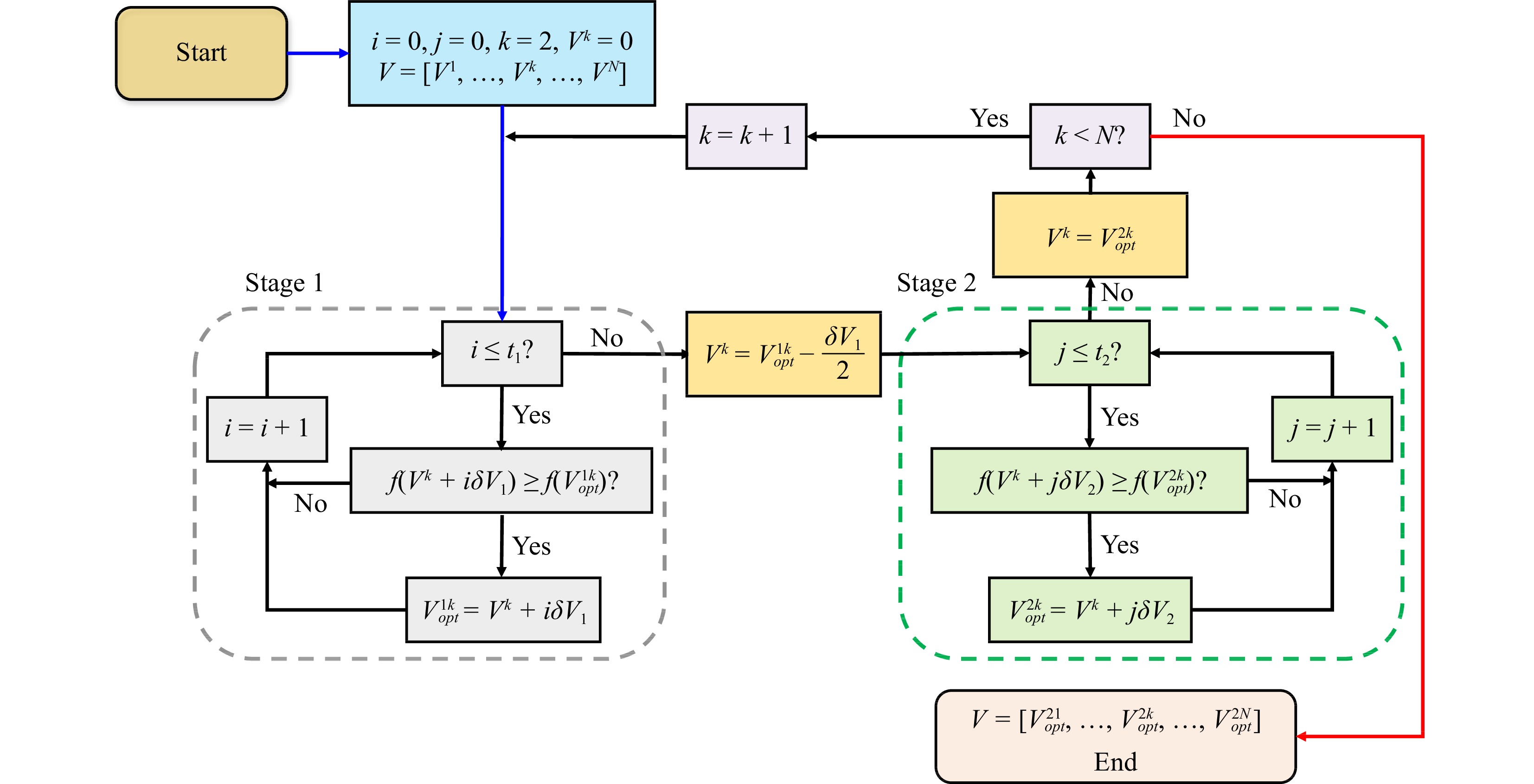
Fig. 2 Flow chart of pointwise optimization approach. In Stage 1,
${V^k}$ is searched in 2π range. In Stage 2, the search scope is greatly reduced. -
Simulations were performed with the specific parameters presented in Table 1 to evaluate the performance of the proposed pointwise optimisation approach.
Parameter Value Wavelength 1550 nm Array scale 1×8 Element interval 20 μm Array width 8 μm Half-wave voltage [4.5, 3.8, 3.6, 3.4, 4.2, 3.4, 4.4, 3.2] V Input voltage range [0, 10] V Table 1. Simulation parameter settings
A simulation was conducted to verify the normalisation diffraction efficiency of the far-field distribution with the change in input voltage, shown in Fig. 3. In addition to the diffraction efficiency, a simulation of the normalisation sidelobe suppression ratio was designed. The sidelobe suppression ratio is defined as the light intensity ratio between the main lobe and the average sidelobe, indicating the far-field intensity distribution change. The simulation results were also compared with the diffraction efficiency curve in Fig. 3.

Fig. 3 Normalisation diffraction efficiency and sidelobe suppression ratio of different elements. Their trend is consistent.
This simulation focused on the first stage of the proposed approach. Fig. 3 shows the curves of the normalisation diffraction efficiency and sidelobe suppression ratio in the first stage. The step size
$\delta {V^1}$ is 0.2 V and iteration times t1 are 50. The total number of iterations for the seven array elements was 350.The above simulations reveal that the pointwise optimisation approach improves the OPA’s diffraction efficiency and sidelobe suppression ratio. In addition, in the iteration process, the far-field diffraction efficiency data curves for the seven modulation elements are similar to sine waves, which is also observed in the curve of the sidelobe suppression ratio. It is evident that the suppression ratio reaches its maximum when the corresponding light intensity reaches the climax, the uniformity of which shows the effectiveness of the pointwise optimisation approach in energy diffraction.
To further evaluate the feasibility of the proposed approach, a comparative simulation was conducted with a typical optimisation approach in adaptive optics, named the Chaos-Stochastic Parallel Gradient Descent (CSPGD) approach. CSPGD approach comprises chaos theory and SPGD algorithm. The chaos part searches for an appropriate set of initial input voltages, whereas the SPGD part iterates for optimal results. It combines the non-repetitive ergodic characteristic of chaotic research and the advantage of a quick search in the SPGD algorithm.
The simulations were conducted as described below. Fig. 4a shows the diffraction efficiency curves of the two approaches under the same iteration times. In the pointwise optimisation approach, the iteration times t1 and t2 are 30 for each array element. In the CSPGD approach, the number of iterations for the chaotic part is 294, while that for the SPGD part is 126. The total number of iterations for both approaches was 420. The diffraction efficiency of the proposed approach improves steadily when the element phases are calibrated separately. The diffraction efficiency of the proposed approach was 28.68%, whereas that of the CSPGD approach was 27.34%. After the calculation is completed, the proposed approach reaches a higher theoretical limit and increases the diffraction efficiency by approximately 4.9%.
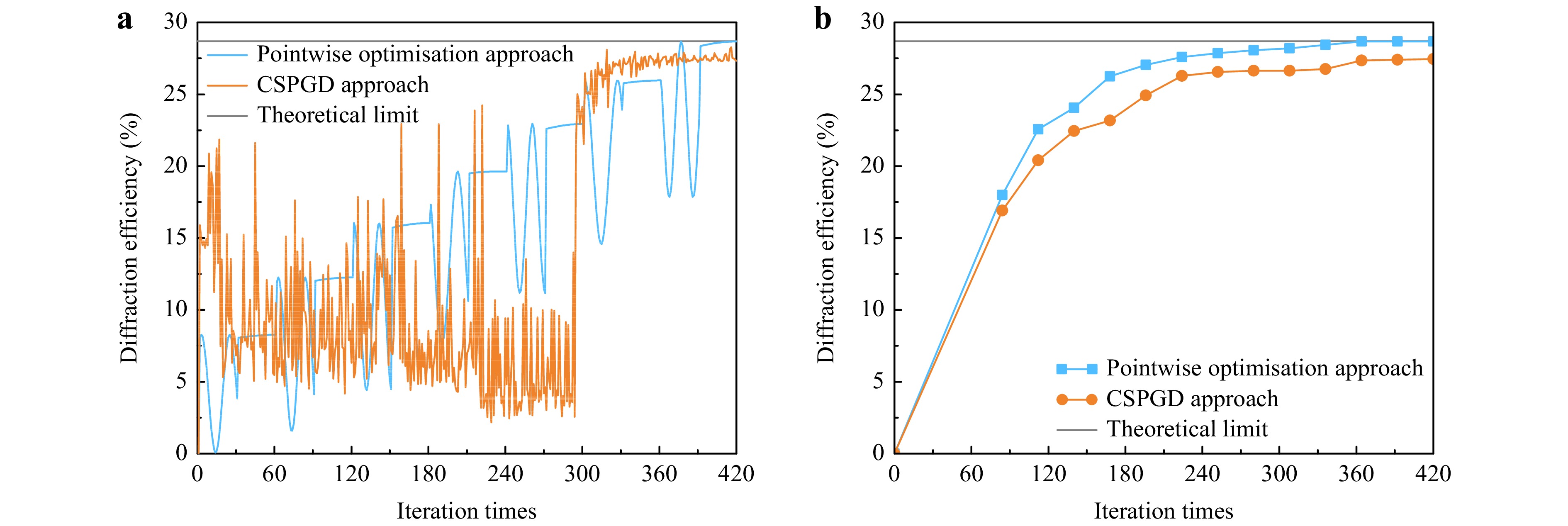
Fig. 4 a Simulation of two calibration approaches in diffraction efficiency. b Simulation of two calibration approaches in convergence rate.
Fig. 4b shows the optimised diffraction efficiency results of the two approaches for different iteration times. t1 and t2 both ranged from 6 to 30; thus, the total number of iterations ranged from 84 to 420. The target diffraction efficiency was set to 27.25%, 95% of the theoretical diffraction efficiency, and polynomial fitting was performed. Thus, the proposed approach reaches the target diffraction efficiency with only 194 iterations, whereas the CSPGD approach, with approximately 395 iterations, indicates a more rapid convergence speed of approximately 50.9%. An average improvement of 6.7% in the diffraction efficiency was also observed, while the two approaches were under the same number of iterations.
Generally, the proposed approach has rapid convergence and a high diffraction limit.
-
The above approach is easy to implement in simulations but requires a mechanical structure to be realised experimentally. The corresponding experimental device was designed before the experiments. Each array element must be selected to realise the pointwise optimisation approach, and an independent modulation voltage must be input for the subsequent iteration process.
Two element selection methods were considered to realise the selection of different array elements to be calibrated, as shown in Fig. 5.
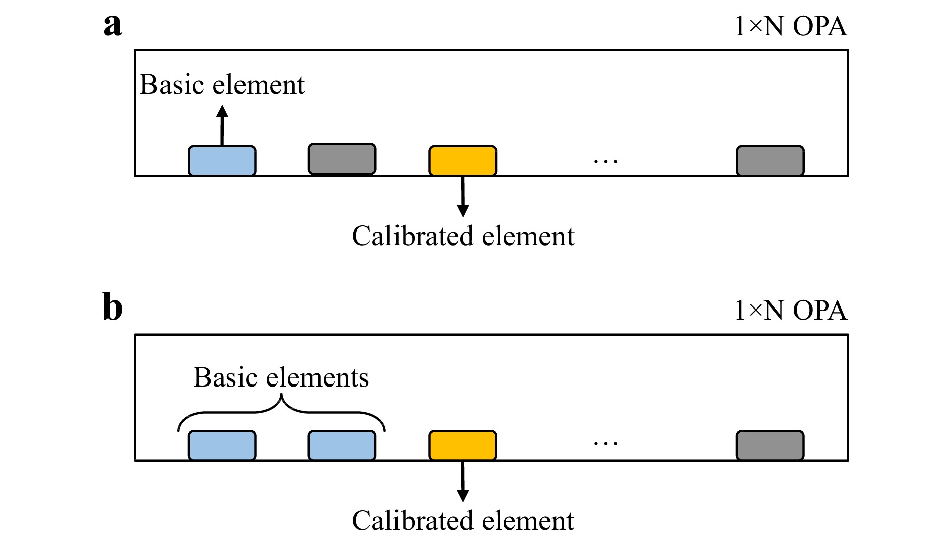
Fig. 5 a Element selection method where the target element interferes with the first element. b Element selection method where the target element interferes with all previous elements. The second method was applied here.
In Fig. 5a the element to be calibrated interferes with the first element, whereas in Fig. 5b the element to be calibrated interferes with all previous elements. With only two elements interfering throughout the procedure, the first selection method avoids phase-accumulation errors when the number of array elements increases. However, the far-field intensity distribution of the first method is too weak to be detected, causing signal acquisition and processing difficulties. Therefore, the second selection method was applied for the benefit of data collection.
Some researchers have applied optical switches based on integrated waveguide30 to realise element selection. Here, we control the phase of the OPA using a mechanical system to realise the method shown in Fig. 5b. A precise displacement device and other mechanical structures compose this mechanical system. As shown in Fig. 6, the system was designed to block the exit beam of the OPA elements one by one through a displacement pulse.
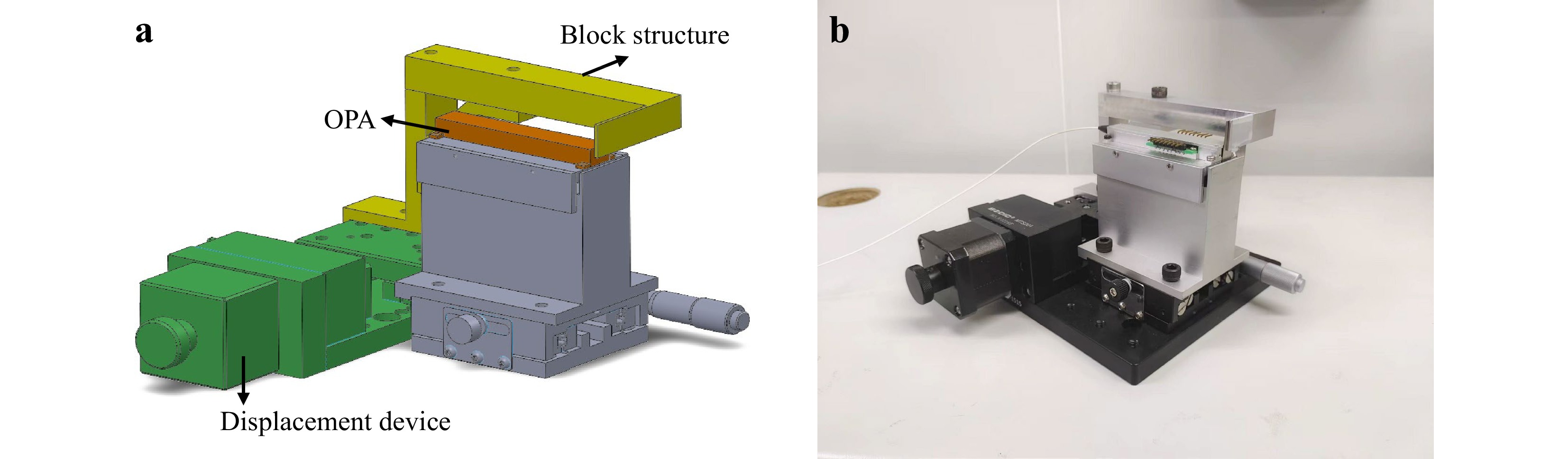
Fig. 6 Mechanical system for elements selection in a and its practical structure b. Element of OPA is selected through the movement of blocked structure, which is driven by a displacement device.
Experiments were conducted with the designed mechanical system to discuss the validity of the proposed approach. Fig. 7 shows the general phase calibration system, with the specific parameters listed in Table 2. The light source was a 1550 nm laser beam generated by an optical amplifier. The OPA is a one-dimensional phase array with eight modulation elements, and an electrode spacing is 20 μm with gap width 12 μm. The far-field diffraction pattern was captured using a CCD infrared camera (GH-SCS-02) with 320 × 256 pixels and uploaded to the computer terminal. The pointwise optimisation approach was applied to generate new element voltages and update the far-field intensity distribution using a D/A converter (PCI-1724U).
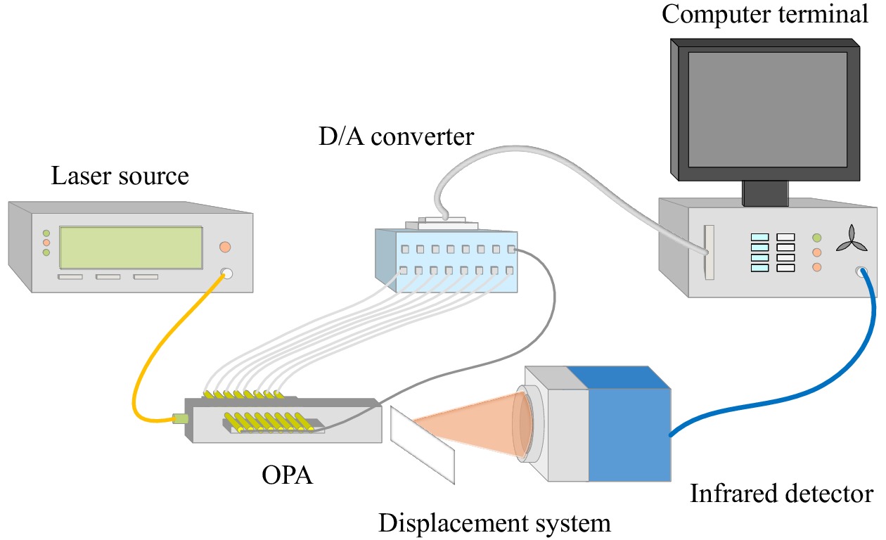
Fig. 7 Setup diagram of OPA phase calibration system.
Parameter Value Waveguide material LiNbO3 CCD area 9.6 mm×7.68 mm Distance from OPA to CCD 20 mm D/A resolution 14 bit D/A voltage range [0, 10] V Table 2. Parameter settings
To evaluate the feasibility of the phase-calibration system, we calculated the diffraction efficiency at the target deflection angle and compared it with the simulation data, as shown in Fig. 8. Fig. 8 shows the curves of the normalisation diffraction efficiency and sidelobe suppression ratio in the first stage. The step size
$\delta {V^1}$ is 0.2 V, and iteration times t1 are 50. The total number of iterations for the seven array elements was 350. The experiment was repeated five times.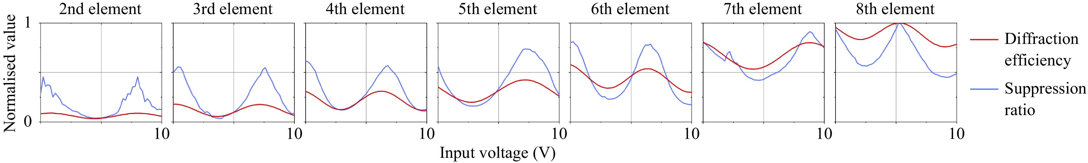
Fig. 8 Normalisation diffraction efficiency and sidelobe suppression ratio of different elements. Their consistency proves the validity of phase calibration system and approach.
According to the results, the change in the far-field intensity is consistent with the simulation results, which verifies the reliability of the phase calibration system. However, an accumulative error caused by the motion of the displacement system was observed, which inevitably led to a deviation in the experimental curves of the subsequent elements.
The sidelobe suppression ratios of the seven elements are also presented in Fig. 8. With the suppression ratio at the peak, the relative diffraction efficiency tends to reach its maximum, maintaining credible consistency and indicating that the pointwise optimisation approach is effective in improving the distribution of the far-field diffraction pattern.
The pointwise optimisation approach is divided into the former and latter stages for each element to decrease the number of iterations. However, the division in the phase calibration process introduces the problem of iteration assignment to different stages. The effects of different voltage steps on the diffraction efficiency were studied to solve this problem, as shown in Fig. 9a.
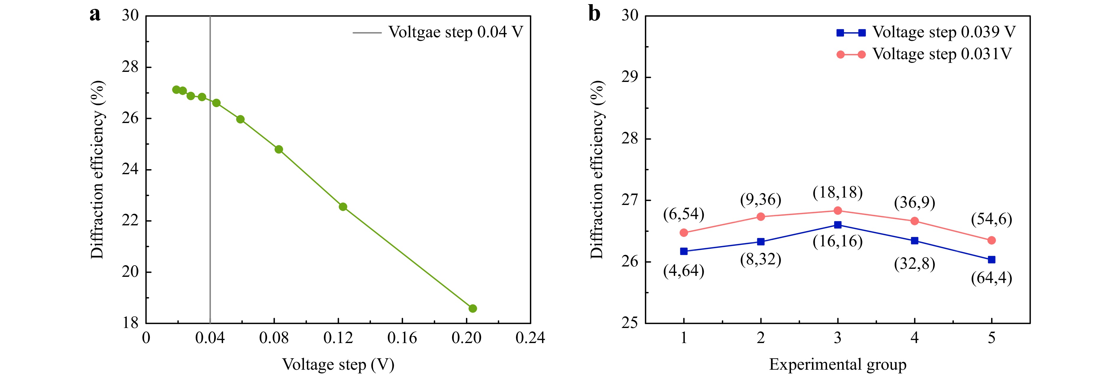
Fig. 9 a Relationship between voltage step and diffraction efficiency. b Relationship between iteration assignment to different stages and diffraction efficiency. The numbers in parentheses represent different iteration times in two stages.
In Fig. 9a, pointwise optimisation with only the former stage was conducted for each array element. The scanning voltage
${V^k}$ sweeps from 0 V to${V_{2\pi }}$ with different step sizes$\delta {V^1}$ ranging from 0.02 to 0.2 V. It is evident that the diffraction efficiency decreases with increasing voltage step. When the step size$\delta {V^1}$ exceeds approximately 0.04 V, diffraction efficiency displays a more rapid decline, based on which we decide the iteration assignment for each stage.As shown in Fig. 9b, we conduct two groups of experiments whose iteration times of the two stages are designed with reference to a 0.04 V voltage step. The
$\delta {V^2}$ of Group 1 was approximately 0.031 V, and that of Group 2 was 0.039 V. The number of iterations t1 and t2 is indicated in parentheses. In Group 1, t1 ranges from 6, 9, 18, 36, and 54, while t2 ranges from 54, 36, 18, 9, and 6, which is also the case in Group 2. In each group, the voltage step$\delta {V^2}$ remains unchanged because the products of t1 and t2 remain the same.It is significant that the closer the number of iterations of the two stages, the higher the diffraction efficiency. The peak far-field diffraction efficiency occurs when t1 and t2 are equal, demonstrating the effectiveness of the pointwise optimisation approach with the least number of iterations. In other words, the same number of iterations should be assigned to the former and later stages. This conclusion was applied in the following experiments.
More experiments were carried out between CSPGD and the proposed approach under conditions of the same iteration times, as shown in Fig. 10. The iteration times of the pointwise optimisation approach for the former and latter stages are equal.
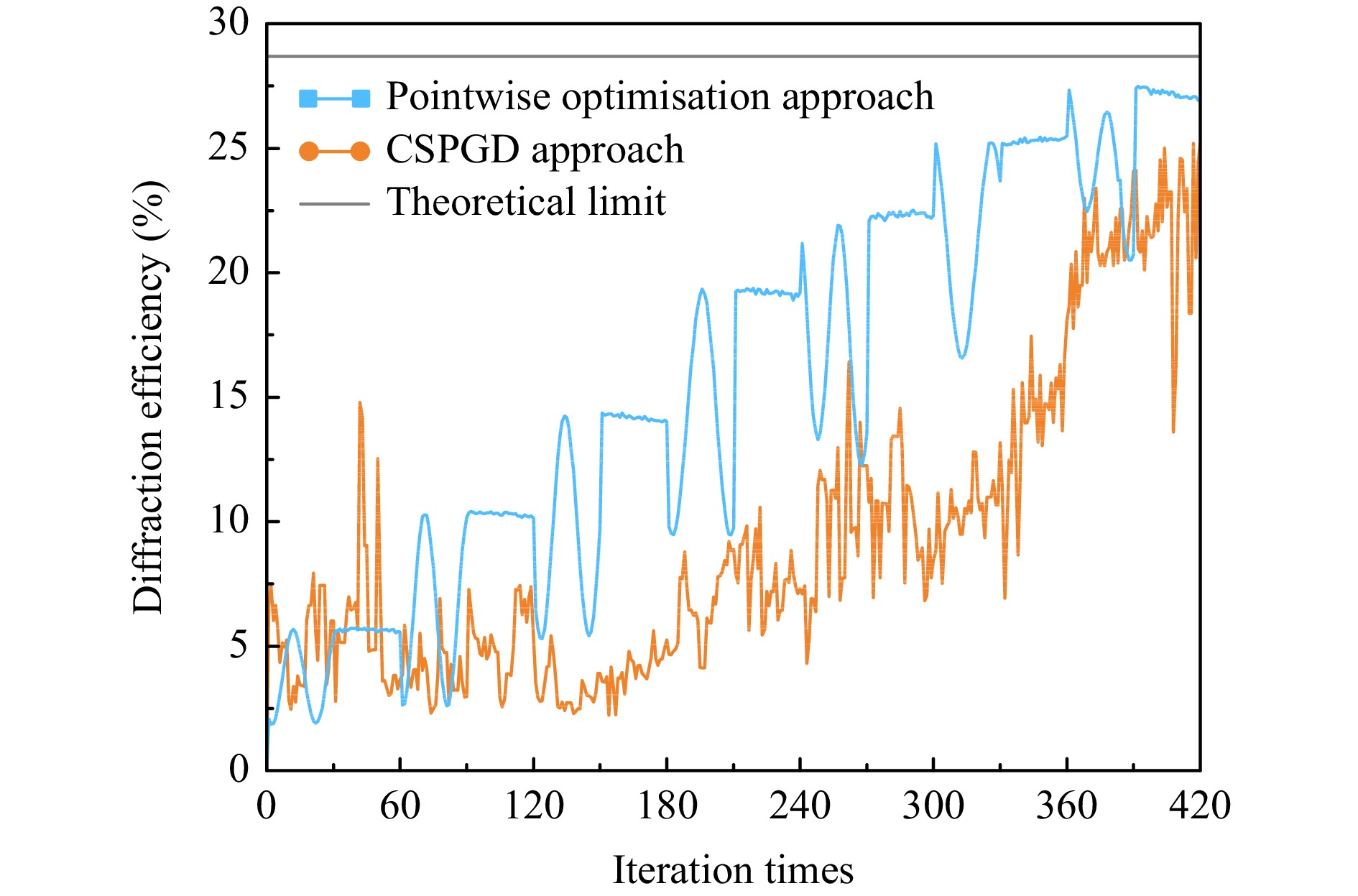
Fig. 10 Comparative experiment on iteration process. It shows the iteration process of the pointwise optimisation approach and CSPGD.
The specific phase calibration process of the two approaches is presented with 420 iterations. In the proposed approach, the number of iterations t1 is 30 and t2 is 30 for each array element. In the CSPGD approach, the number of iterations for the chaotic part is 294, and that for the SPGD part is 126.
In the CSPGD approach, although the general tendency of the diffraction efficiency gradually increases, the iteration process is uncertain, and the optimised result is poorer. The diffraction efficiency of the CSPGD approach was 25.22%, whereas that of the proposed approach was 27.48%. The proposed approach reaches a higher theoretical limit and increases the diffraction efficiency by approximately 9.0%. Owing to the inaccuracy of the D/A converter and the voltage error, the convergence rate of the CSPGD is inconsistent with the simulation result. However, the phase-calibration result of the proposed approach is still compliant with the simulation, indicating that the pointwise optimisation approach has the merit of robustness when compared with CSPGD.
More experiments are designed from the aspects of programme running time and diffraction efficiency under the condition of different iteration times. In the proposed approach, t1 and t2 range from 6 to 30. The total number of iterations of the two approaches ranged from 84 to 420.
Fig. 11a shows that the two stages of iteration reduce the computational cost, thus contributing to the shorter programme running time. Generally, the running time of the pointwise optimisation approach decreased by approximately 9.7%.
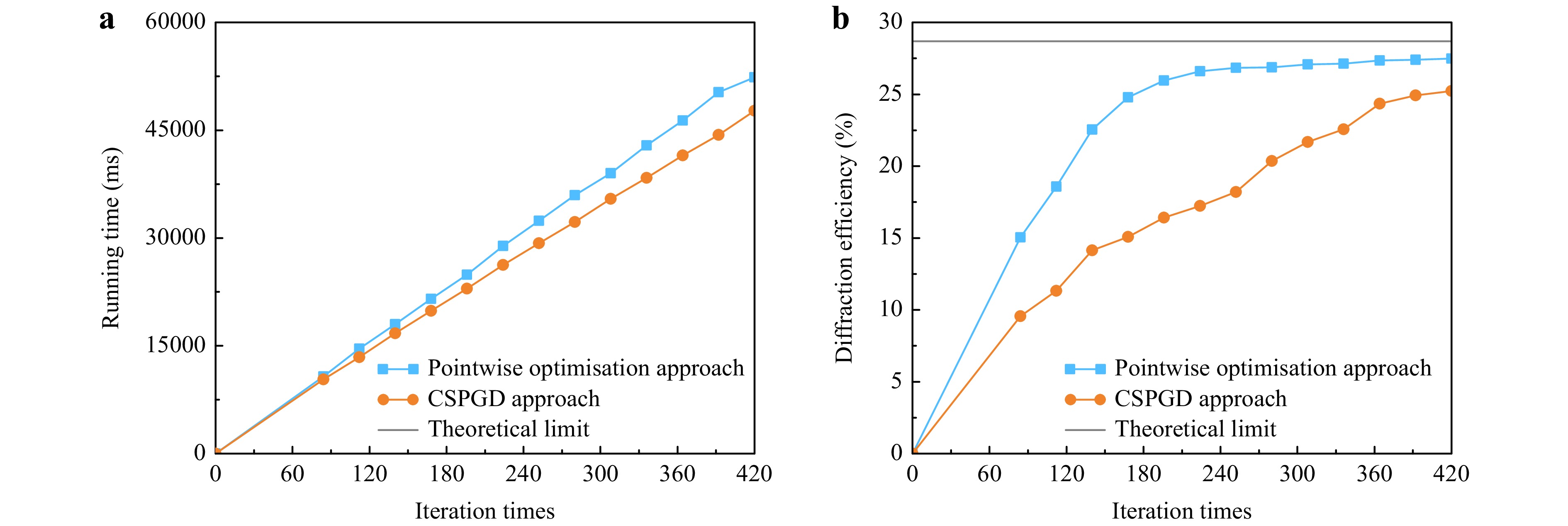
Fig. 11 Comparative experiment on a programme running time and b diffraction efficiency at different iteration times.
Apart from a shorter running time compared to the CSPGD optimisation, as shown in Fig. 11b, the pointwise optimisation approach shows a better convergence rate. The proposed approach reached a target diffraction efficiency of 25% with only 186 iterations, whereas the CSPGD approach showed approximately 400 iterations under polynomial fitting. The proposed approach demonstrated a rapid convergence speed of approximately 53.5%. This also indicates an average improvement of 39.5% for the same number of iterations. Meanwhile, the pointwise optimisation approach achieves better-optimised results at all iteration times, demonstrating its rapid convergence and precise calibration.
-
The proposed simulation and experimental results demonstrate that the pointwise calibration approach achieves rapid and precise phase calibration. With the help of carefully designed mechanics, the pointwise calibration approach realises the selection of different elements. It is a type of deterministic approach that improves the diffraction efficiency of the OPA. It combines the characteristics of global search and accurate calibration and significantly decreases the number of iterations. Proper division in the phase calibration process also reduces the computational cost.
Furthermore, when compared with the typical adaptive optical approach, CSPGD, the proposed pointwise calibration approach still shows excellent performance in terms of convergence rate and energy efficiency. The experimental result of the pointwise calibration approach is much closer to the simulation data, indicating its advantage in robustness.
In conclusion, the pointwise optimisation approach is efficient and reliable for improving beam steering and focusing. The proposed approach performs rapid and deterministic phase calibration using a pointwise and segment correction process, which can be potentially cost-effective and high-performance OPA. This approach has shown practical value in autonomous vehicles and LiDAR.
-
This work was partly supported by the National Natural Science Foundation of China under Grant Nos. 61922011 and U21B2034, partly by the Open Research Projects of KLOMT under Grant No. 2022KLOMT02-02.
Fast and deterministic optical phased array calibration via pointwise optimisation
- Light: Advanced Manufacturing 4, Article number: 10 (2023)
- Received: 04 November 2022
- Revised: 02 April 2023
- Accepted: 03 April 2023 Published online: 19 April 2023
doi: https://doi.org/10.37188/lam.2023.010
Abstract: Owing to the structural errors in the optical phased array, an initial random phase reduces the quality of the deflection beam. The most commonly applied approach to phase calibration is based on adaptive optics. However, adaptive optimisation approaches have slow convergence and low diffraction efficiency. We proposed a pointwise optimisation approach to achieve fast and accurate beam deflection. This approach conducts phase calibration, combining global traversal and local searches individually for each array element. We built a phase-calibration optical system containing a one-dimensional optical waveguide phase array for further verification and designed the relevant mechanics. The simulation and experimental results demonstrate that the pointwise optimisation approach accelerates the calibration process and improves the diffraction efficiency.
Research Summary
Phase calibration: Accurate beam steering improves OPA’s performance
Beam steering technology based on optical phased array (OPA) is promising in the applications of environmental monitoring, LiDAR, autonomous vehicles and many other fields. OPA utilizes the electro-optical (EO) or thermo-optical (TO) effect of the anisotropy crystal material modulators to adjust additional phase difference between the array elements, and thus regulates the deflection direction of the beam without mechanical components. However, the existence of random phase noises induced by structural errors, greatly limits the steering accuracy and deflection efficiency of OPA. Professor Ming-Jie Sun and students from Beihang University reported a pointwise optimisation approach to achieve deterministic and fast control of the deflected beam. This approach combines the advantages of global search and accurate calibration, and the prototype optical system demonstrated in this paper can be further applied in driving and controlling OPA all-solid-state LiDAR.


Rights and permissions
Open Access This article is licensed under a Creative Commons Attribution 4.0 International License, which permits use, sharing, adaptation, distribution and reproduction in any medium or format, as long as you give appropriate credit to the original author(s) and the source, provide a link to the Creative Commons license, and indicate if changes were made. The images or other third party material in this article are included in the article′s Creative Commons license, unless indicated otherwise in a credit line to the material. If material is not included in the article′s Creative Commons license and your intended use is not permitted by statutory regulation or exceeds the permitted use, you will need to obtain permission directly from the copyright holder. To view a copy of this license, visit http://creativecommons.org/licenses/by/4.0/.

 DownLoad: