


-
When light interacts with a medium, changes in intensity and phase occur simultaneously1. Conventional image sensors can only capture the intensity of the light field. In contrast, the phase of the light field offers more multidimensional information in many application scenarios2,3, including biological imaging1, heat characterization4, patterned wafer inspection5,6, and material metrology7. Quantitative phase imaging (QPI) is a non-invasive and label-free measurement method that accurately determines phase profiles induced by light transmission through medium1,8–15. In many cases, QPI requires a traditional microscope structure7, which inherits the two interrelated yet conflicting features, i.e., the field of view (FOV) and the optical resolution16. The conventional solution to tackle the challenge of large-area measurements in microscopy is to divide the extensive area into smaller regions, allowing multiple measurements (such as large-scale cellular analysis17–21 and patterned wafer defect inspection22–24). However, this approach is time-consuming due to the requirement of step mode and image stitching. To enable wide-field imaging, researchers have proposed several alternative techniques, including Fourier ptychographic microscopy25,26, synthetic aperture microscopy27,28, multi-lens array microscopy29, and lensless computational imaging30, which usually come at the expense of speed. To enhance imaging speed, QPI was improved by refining image acquisition methods, including multi-channel imaging31–33 and scanning holography34–38, but this is typically achieved at the expense of FOV. In conclusion, a QPI technique that could overcome the conflict between resolution and FOV is very important to the field.
In this paper, we developed a novel QPI technique called Lateral Line-scan Computational Phase Imaging (L2-CPI), which fuses a novel pixelated data-acquisition strategy, a horizontal phase-shifting technique, and a robust phase reconstruction algorithm to enable a theoretically arbitrarily large FOV without sacrificing the optical resolution36,39. Fig. 1a presents a schematic of the comparison between L2-CPI and conventional QPI techniques, in which the upper half depicts the feature of a traditional QPI in measuring the 3D profile of a large-area sample, i.e., FOV-limited phase images are captured at different positions, followed by image stitching. In contrast, L2-CPI could image the profile of the entire sample in a single consecutive scanning process (we call it a single consecutive FOV); see the lower half of Fig. 1a. While image stitching is a common and mature strategy for measuring large-scale samples, its application in QPI often leads to two typical types of errors: overlap and misalignment of the reference phase between adjacent images, which we refer to as “near error”. More details can be found in Supplementary 9. In contrast, L2-CPI is a “near error-free” measurement method that does not require any post-processing registration. A dynamic compensation system (DCS) is developed for L2-CPI to dynamically compensate for the offset in the interference fringes induced by pitch and yaw errors during lateral scanning of samples40, thereby guaranteeing high-quality phase imaging throughout the scanning process. We experimentally demonstrated that L2-CPI could achieve the precise phase imaging of transparent and opaque samples with a large FOV, limited only by the scanning range of the sample stage. Meanwhile, its resolution is the same (i.e., diffraction-limited) as that of conventional quantitative phase microscopes. The maximum FOV in conventional QPI is constrained by the objective lens, as illustrated in Fig. 1b, where achieving a larger FOV often necessitates sacrificing resolution by opting for a lower magnification lens; in contrast, L2-CPI enables unlimited expansion of the FOV while maintaining the flexibility to select hardware for various resolutions, overcoming the limitations of conventional QPI techniques. We hope that L2-CPI can serve as a fundamental platform for fast and large-area phase imaging in diverse fields such as bioimaging, nanosensing, 3D metrology, and semiconductor inspection.
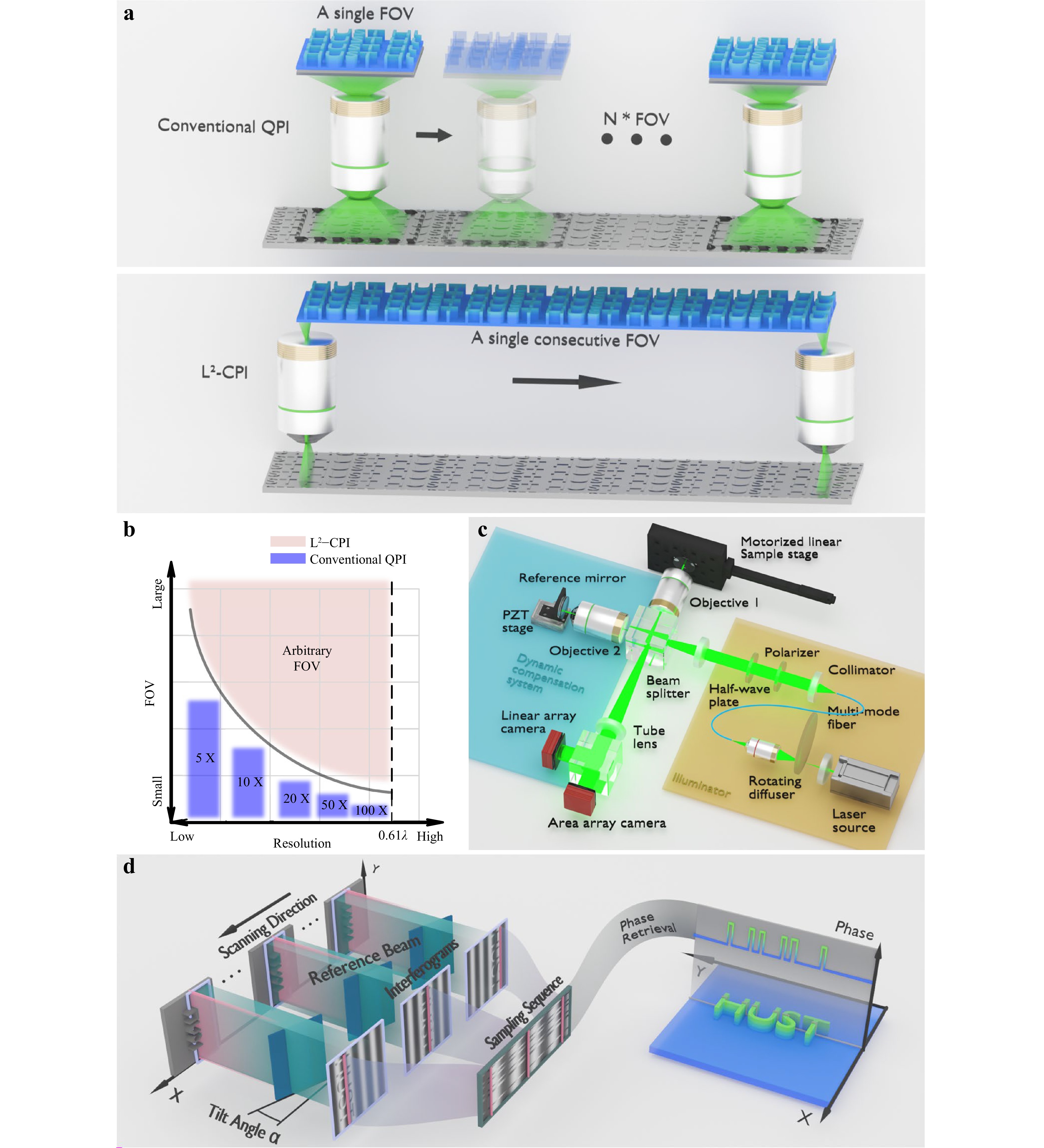
Fig. 1 Principle and system configuration of L2-CPI. a The schematic diagram illustrating the difference between L2-CPI and the conventional QPI. b The relationship between resolution and FOV in conventional QPI and L2-CPI. 0.61λ represents the theoretical maximum achievable resolution limit by conventional dry optical microscopy systems. The blue box delineates the range of field of view (FOV) and resolution capabilities attainable with objective lenses of varying magnifications. In contrast, the gray curve illustrates the FOV limits imposed by these lenses at different magnifications. c The optical configuration of L2-CPI. d The schematic diagram illustrating the data acquisition process of L2-CPI. The gray structures on the left represent the sample, which consists of four letters: “HUST”. The purple boxes on the sample represent the imaging area, which corresponds to the camera’s sensing area. As the sample moves along the scanning direction, many interferograms are captured. See the three representative interferograms corresponding to the sample’s three positions along the scanning direction (i.e., x-axis) in Fig. 1d. The three red lines in the three interferograms correspond to precisely the same positions (i.e., the cross-sections along the y-axis) on the sample’s surface. For a given cross-section on the sample’s surface, its corresponding interferogram lines (i.e., the red lines) in all the interferograms are extracted to form a sampling sequence (i.e., see the dark green box marked by “sampling sequence” in Fig. 1d) in first-come-first-served order. The phase retrieval algorithm can then be applied to the sampling sequence to retrieve the phase corresponding to the cross-section on the sample’s surface.
-
L2-CPI consists of two modules: the interferometer module and the dynamic compensation module, as shown in Fig. 1c. The interferometer module features a typical Linnik configuration, comprising two objectives that generate interference fringes. The dynamic compensation module consists of an actuator, a reference mirror, and a linear array camera, which is used to dynamically compensate for the offset in the interference fringes during the lateral scanning of the sample. A single longitudinal-mode laser provides coherent illumination at a single wavelength in the interferometer module. To mitigate laser speckles, a rotating diffuser and a multi-mode fiber are utilized to homogenize the laser beam. The input light beam is split into two beams (i.e., the sample beam and the reference beam) using a beam splitter. The sample beam passes through the objective lens and is reflected after interacting with the sample, which is placed on a motorized stage. The reference beam is reflected from a mirror mounted on a kinematic mount. The reference beam and the sample beam are combined to generate the interferogram, which is captured by the area array camera positioned at the rear focal plane of the tube lens. Notably, the reference mirror is intentionally tilted by a slight angle α with respect to the optical axis, causing the wavefront of the reference light to also form an angle α with respect to the optical axis. As a result, a slowly varied phase shift is introduced into the reference wavefront along the scanning direction of the sample (see the schematic in Fig. 1d). If the sample is scanned along the scanning direction shown in Fig. 1d, the horizontal phase shift is simultaneously introduced in the interferograms captured by the array camera. The image captured by the camera along with the scanning direction (i.e., x-direction in Fig. 1d) of the sample can be represented as
$$ \begin{aligned}I\left(x,y\right)&=A\left(x,y\right)+B\left(x,y\right)\cos \left[\phi \left(x,y\right)+\Delta \varphi \left(x\right)\right]\\ \Delta \varphi \left(x\right)&=\frac{4{\text{π}} }{\lambda }x\tan \alpha \end{aligned} $$ (1) where I(x,y) is the interferogram, A(x,y) is the average intensity, B(x,y) is the intensity modulation of the interference between the two beams, and ϕ(x,y) represents the phase distribution. The phase shift, denoted as Δφ(x), is a linear function of the x coordinate, which is also the direction in which the reference beam is tilted. As a result, scanning the sample horizontally will generate a complete phase shift; see the schematic in Fig. 1d. The key of L2-CPI is that the lateral scanning of the sample simultaneously realizes a large FOV and phase shift. The frame rate f of the camera should match the speed v of the sample stage, i.e., v/f = w/M, where w is the width of a pixel of the camera, and M is the magnification factor of the microscopic system (for the simplicity of clarity, we assume M = 1 in the following). As a result, the camera captures a frame of the interferogram of the sample as the stage moves by one pixel along the x direction (see the Cartesian coordinate system in Fig. 1d). Because an angle α tilts the reference beam, the phase shifts of the reference beam at different positions along the scanning direction of the sample are also different. This indicates that N different sample positions along the scanning direction correspond to N different phase shifts. N interferograms are captured as the sample moves by a length of N × w along the scanning direction (i.e., the x-axis in Fig. 1d). See the three representative interferograms corresponding to the sample’s three positions along the scanning direction in Fig. 1d. The three red lines in the three interferograms correspond to the same positions (i.e., the cross-sections along the y-axis) on the sample’s surface. For an arbitrarily given cross-section on the sample’s surface, its corresponding interferogram lines (i.e., the red lines) in all the interferograms are extracted to form a sampling sequence (i.e., see the dark green box marked by “sampling sequence” in Fig. 1d) in first-come-first-served order. The phase retrieval algorithm can then be applied to the sampling sequence to retrieve the phase corresponding to the cross-section on the sample’s surface. See more details on the acquisition of images in Supplementary 1.
To mitigate phase shift disturbances caused by the motorized stage’s pitch and yaw errors during scanning, the reference mirror is mounted on a piezoelectric transducer (PZT) stage that dynamically oscillates. A high-speed linear array camera captures interference fringe signals identical to those of an area-array camera through a beam splitter positioned behind the tube lens. These signals are used for DCS feedback in real-time (see more details in the Section “Dynamic compensation system”).
-
Multi-step phase-shifting algorithms are widely used for phase retrieval41. Traditional phase shift algorithms exhibit high sensitivity to vibrations due to their limited capacity to filter noise from a limited number of calculation points. Moreover, these algorithms necessitate a predefined phase-shifting value, such as π/4 or π/3. However, because the absolute phase-shifting values cannot be directly determined if we cannot accurately control the tilting angle of the reference mirror, L2-CPI cannot guarantee the precise phase-shifting values. Moreover, inevitable vibrations occur when the sample scans to generate the desired phase shift, making the determination of phase-shifting values more challenging. As a result, L2-CPI cannot use the conventional multi-step phase-shifting algorithms. However, the intensity variation of the sampling sequence, obtained by scanning along the sampling direction (i.e., stacking order of the interferogram line, consistent with the acquisition order of the interferograms), displays a periodic pattern analogous to that of a trigonometric function. Moreover, despite the unknown sampling step (defined as the phase-shifting value between two interferogram lines in the sampling sequence) throughout the scanning process, the uniform motion displacement applied in the pixel-by-pixel scanning method ensures that the sampling step for the entire sampling sequence remains relatively stable. To retrieve the phase from the sampling sequence, we employ a fast three-parameter cosine fitting algorithm42 to analyze the intensity variations induced by phase shifts across all interferograms. This algorithm is inherently robust to minor vibrations and uneven speeds of the linear stage because it accommodates many data points43. The fitting algorithm leverages the known sampling step, significantly improving the speed (see its comparison with the four-parameter cosine fitting algorithm in Supplementary 2) and effectively mitigating the influence of vibrations. Moreover, the calculation can be further simplified if the sample length of the sampling sequence used for fitting is an integer multiple of the cosine period. The phase at this point, which is denoted as ϕ, can be expressed as follows:
$$ I\left(t\right)=a\cos \left(t\omega \right)+b\sin \left(t\omega \right)+A+n $$ (2) $$ \phi =\arctan \frac{-\sum\limits_{t}I\left(t\right)\sin \left(t\omega \right)}{\sum\limits_{t}I\left(t\right)\cos \left(t\omega \right)} $$ (3) where I(t) is the intensity at a point in the sequence across all interferogram lines, ω is the sampling step, and n is the intensity variations that arise from random errors generated by the camera and rotating diffuser, as well as the random offsets of interference fringes in the interferograms, which are caused by mechanical vibrations of the sample stage. The DCS can suppress most system noise, leaving only minor random noise. More details regarding the derivation of this formula can be found in Supplementary 3. Once the tilting angle of the reference mirror is fixed, the sampling step remains constant regardless of the horizontal displacement of the sample stage. As a result, given that the step of the sampling sequence is estimated beforehand (i.e., using a four-parameter cosine fitting algorithm for estimation), the fitting process is linear, which is intrinsically fast. As shown in Fig. 2a, the running speed of the three-parameter cosine fitting algorithm is comparable to that of the conventional 7-step phase-shifting algorithm, even though the number of data points is approximately 100 times larger. More details about the traditional 7-step phase-shifting algorithm can be found in Supplementary 4. Due to the increased number of data points, the fitting algorithm can somewhat suppress random noise. To characterize the phase sensitivity of the proposed L2-CPI, we selected an unetched area on a silicon wafer for measurements, as shown in Fig. 2b. We compared the phase imaging results reconstructed by the 7-step phase-shifting algorithm44 with those reconstructed by the fast three-parameter cosine fitting algorithm. Moreover, we also compared the fast three-parameter cosine fitting algorithm-based L2-CPI with digital holographic microscopy (DHM) in terms of the standard deviation (STD) of image noise. The measurement results obtained by the fast three-parameter cosine fitting algorithm-based L2-CPI outperform those obtained by DHM and the 7-step phase-shifting algorithm-based L2-CPI. As shown in Fig. 2b, stripe patterns along the scanning direction and jitter perpendicular to the scanning direction are significantly suppressed in the fast three-parameter cosine fitting algorithm-based L2-CPI.
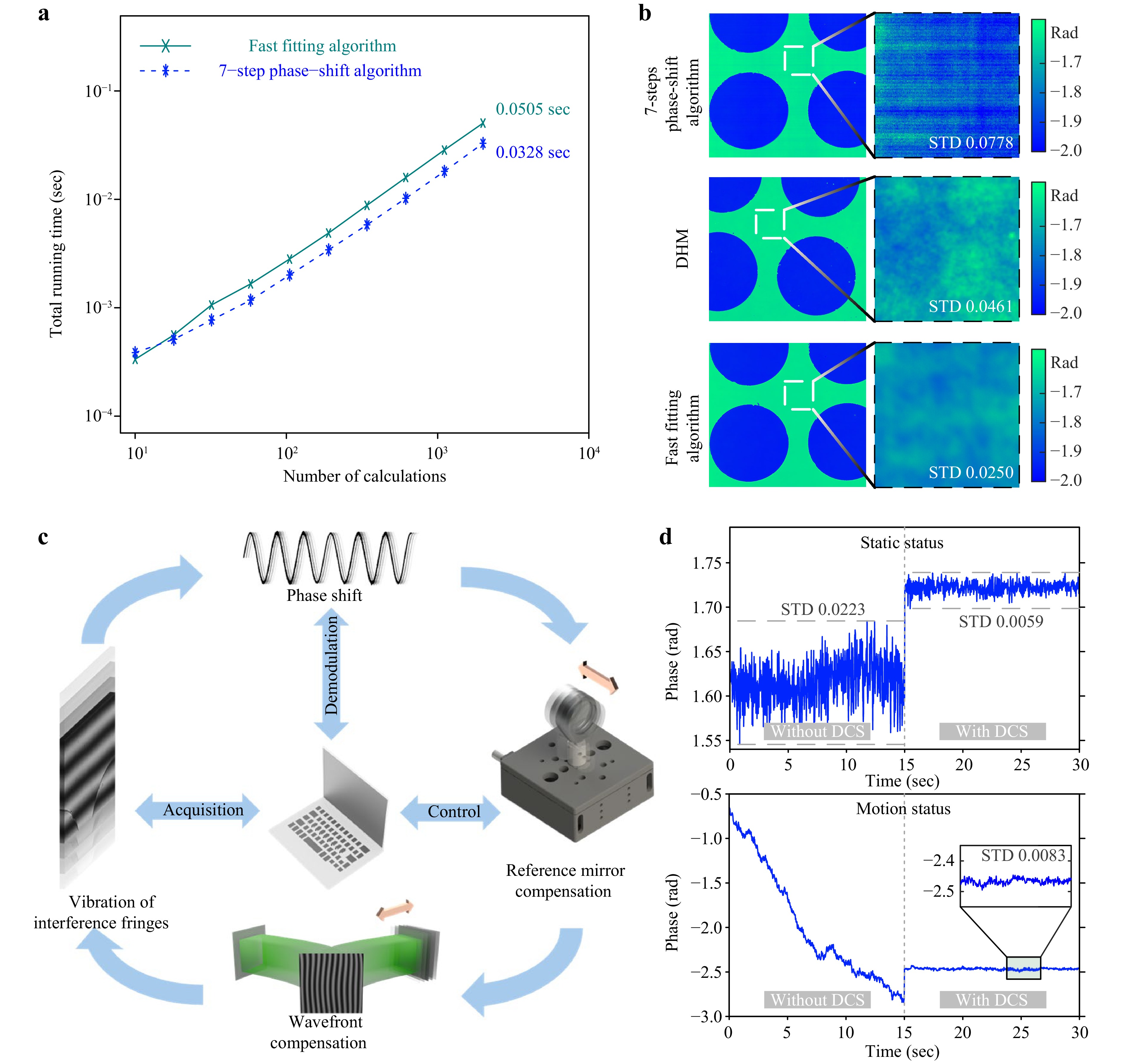
Fig. 2 The working principle of DCS and the fast three-parameter cosine fitting algorithm, and its application in the DCS. a The running time of the 7-step phase-shift algorithm and the fast three-parameter cosine fitting algorithm as functions of the number of calculations. The number of calculations refers to the number of times the phase recovers from the sampling sequence using the algorithms. b The reconstructed phase maps of three techniques and their comparison in terms of STD of an unetched area on the wafer. c The flow chart of the DCS’s working process. d The measured STDs of phase maps without (left) and with (right) DCS at static (upper) and moving (lower) statuses.
-
Because the random vibrations of the sample stage occur throughout the entire scanning process, the reconstructed phase is distorted significantly if there is no error-compensation system. To compensate for the phase error induced by the sample stage’s vibrations, we introduce a DCS that moves the reference mirror axially using an actuator. The dynamic offsets of the interference fringes are first captured by the high-speed linear array camera (see Fig. 1b), after which the fringes are demodulated and converted into the requisite displacement for the reference mirror. Benefitting from the camera’s high frame rate, the system can compensate for fringe vibrations at a high speed. The DCS only needs to utilize the flat area on the sample without the use of additional light sources. According to the principle of interference, it is easy to see that the interference fringe signal collected by the high-speed linear array camera is a cosine signal. The random vibration of the sample stage causing an offset in the interference fringes can be regarded as the phase shift of the cosine signals45,46. The cosine signals I captured by the high-speed linear array camera can be represented as
$$ I=A+B\cos \left[\frac{4{\text{π}} }{\lambda }\left({d}_{r}-{d}_{t}\right)+\frac{4{\text{π}} }{\lambda }\Delta r-\frac{4{\text{π}} }{\lambda }\Delta c\right] $$ (4) where dr − dt is the optical path difference between the reference mirror and sample, Δr is the random vibration that needs to be determined and compensated for the reference mirror, 4πΔr/λ is the phase shift of the cosine function, and Δc is the compensation dosage for vertical random vibration. During the initialization of L2-CPI, the actuator drives the reference mirror to move to the center of the actuator’s stroke, and the fringe information at this position is recorded. Before starting the acquisition process, the DCS is activated to stabilize the fringes. The working process of the DCS is illustrated in Fig. 2c. The high-speed linear array camera captures the interference fringes, after which a fast three-parameter cosine fitting algorithm is utilized to fit the interference signal and determine the phase shift Δφ = 4πΔr/λ of the wavefront for each frame captured by the high-speed linear array camera. The random vibration of the stage Δr can then be determined by a simple linear algebra calculation Δr = Δφλ/4π. The axial movement Δc of the reference mirror can then be set as Δr to compensate for the random vibration induced by the sample stage. Δr will be input into a classical PID controller, which is implemented in Python and communicates with the actuator driver via a serial port. Considering the actuator driver’s maximum response delay of 20 milliseconds, we implemented a lower proportional gain in conjunction with a higher derivative gain to suppress system oscillations and avoid overshoot effectively. Moreover, as the camera operates at a frame rate of 76.8 frames per second (FPS) while the driver’s maximum control frequency is limited to 50 Hz, we employed a multithreading algorithm to enhance the system’s real-time performance and stability, thus preventing data processing bottlenecks. We employ the STD of the demodulated fringe offset over a defined running time as the evaluation criterion. As shown in the upper sub-figure of Fig. 2d, the DCS could significantly reduce the fringe offset by 73.54% compared to the fringe offset captured without using the DCS in the stationary state. As shown in the lower sub-figure of Fig. 2d, a significant fringe offset is observed as a function of time when the sample stage begins to move without the DCS. We observed a substantial reduction in STD by activating the DCS, indicating that the DCS can stabilize the fringe offset to a level comparable to that in the stationary state. This suggests that, regardless of whether the system is in a static or motion state, DCS possesses strong fringe compensation capabilities. Additionally, we believe that as long as interference fringes still exist and the actuators have not exceeded their travel range, even if the system experiences a significant shock causing an instantaneous offset of the interference fringes by more than one period, the DCS can leverage the periodic nature of the interference fringes to quickly lock the fringes onto the preset phase using the nearest neighbor principle. Our current DCS system operates at a modulation frequency of 45 Hz, but significant improvements are possible by upgrading to modern components. By adopting a high-speed actual linear array camera and implementing an open-loop driver specifically designed for the actuator, we can achieve a modulation frequency of up to 2 kHz. Today’s linear array cameras are capable of line rates exceeding 100 kHz, while advanced open-loop drivers (such as the PDM420.1 from NanoMotions Inc.) offer control bandwidths of up to 2 kHz. Given that our algorithm is also capable of running at frequencies above 10 kHz, reaching a modulation frequency of 2 kHz is both realistic and achievable.
-
Compared to conventional QPI systems, L2-CPI could provide ultra-large-FOV phase imaging without sacrificing the optical resolution, making it suitable for the high-resolution measurement of transparent and opaque samples. Here, we present the applications of L2-CPI in 3D profile metrology for both transparent and opaque samples. The optical microscope images of the patterned silicon wafer are shown in Fig. 3a. The height profile of the etched patterns was measured using a commercial white-light interferometer (WLI), and the measured results are shown in Fig. 3b. As a comparison, L2-CPI could capture the entire 3D profile in a single consecutive measurement (i.e., a single consecutive FOV); see the white box representing a single consecutive FOV of L2-CPI in Fig. 3a. Here we should emphasize again that the length of a single consecutive FOV of L2-CPI can be as long as the travel range of the sample stage. The cross-section of a hole measured by the WLI demonstrates that the actual etching depth is 207.1 nm, indicating a 7.1 nm bias from the nominal depth (i.e., 200 nm). We then use the L2-CPI system to measure the phase map of the rectangular area (1,317.1 μm long by 101.4 μm wide) in a single consecutive FOV. The reconstructed phase can be easily converted to the depth information following a simple algebraic equation
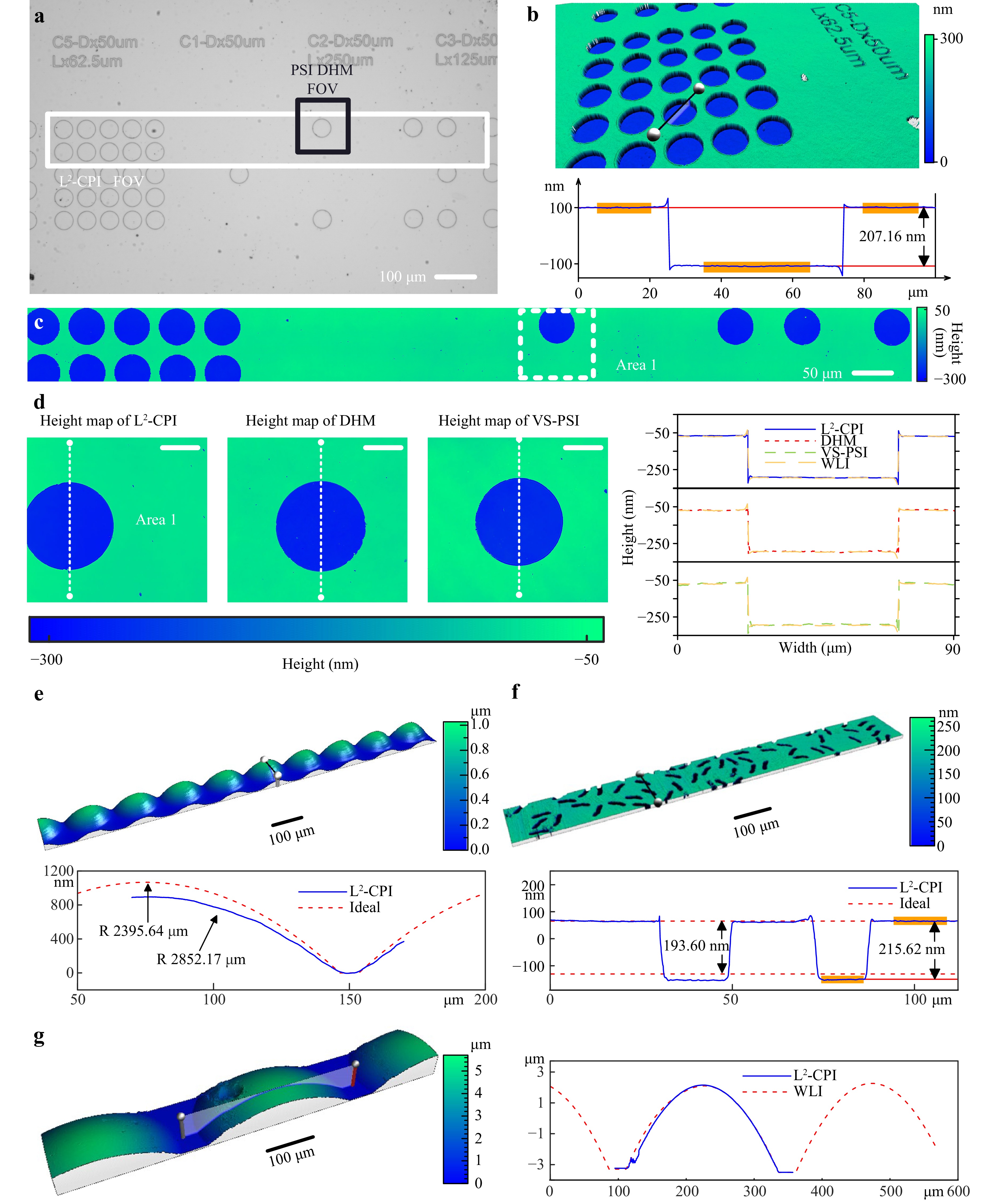
Fig. 3 3D profiles metrology using L2-CPI. a The bright-field microscopy image of the sample. The areas encircled by a white box and a black box represent the single consecutive FOV of L2-CPI and the FOV of DHM and VS-PSI. b The measured 3D profile of the sample using a commercial white light interferometer, which is used as the golden standard for L2-CPI. c The reconstructed 3D profile for a single consecutive FOV of L2-CPI. The result encircled by the white dashed box is compared with that obtained by DHM. d Comparison of measurement results for the same area using L2-CPI, DHM, and VS-PSI. Scale bar: 20 µm. e The reconstructed phase maps of a transparent microlens array, R represents the radius of curvature. f The reconstructed phase maps of a phase calibration slide, the red dashed line indicates the ideal etching depth. g The reconstructed phase maps of a microlens array with an infrared AR coating.
$$ h=\frac{\lambda \phi }{4{\text{π}} } $$ (5) where λ is the wavelength of the light source, ϕ and h are the phase and depth distributions, respectively. See the height map in Fig. 3c. As a comparison, the FOV of a DHM and a vertical scanning phase shift imaging (VS-PSI) using the same hardware configuration of the L2-CPI system is only 92.7 μm×101.4 μm (see the black box representing a single FOV of DHM and VS-PSI in Fig. 3a). The phase retrieval algorithm employed by VS-PSI is the conventional 7-step phase-shifting algorithm, with further details provided in the supplementary 4. The reconstructed heights for the same micro-hole using L2-CPI, DHM, and VS-PSI are nearly identical (L2-CPI: 205.0 nm, DHM: 204.9 nm, VS-PSI: 203.8 nm), demonstrating that L2-CPI can achieve highly accurate 3D surface metrology even during consecutive sample movements (as illustrated in Fig. 3d). Additionally, the measurement results obtained from WLI are presented in Fig. 3d as a reference for the sample profiles. Note that L2-CPI is built upon Linnik interferometry. Thus, L2-CPI can be seamlessly applied to the transparent samples. As shown in Figs. 3e and 3f, L2-CPI could also reconstruct the 3D profiles of a transparent microlens array (MLAS10-F05-P150-AB, LBTEK Inc.) and a phase calibration slide (Phasics Inc.) in a single consecutive FOV (1,402.0 μm long by 101.4 μm wide for the microlens array and 858.8 μm long by 101.4 μm wide for the etched glass substrate). Due to the low reflectivity of the sample surface, the WLI employed in our study was unable to resolve the results consistently. Consequently, we estimated the ideal surface of the sample by utilizing the design parameters of the microlens array and the test report from the phase calibration slide. Further details regarding the ideal surface utilized as a reference are available in the supplementary 6. In Fig. 3e, the phase distribution obtained by L2-CPI spans more than one wavelength range, necessitating phase unwrapping to determine the correct phase distribution accurately. The ideal curvature radius of the transparent microlens array is 2,395.64 μm, whereas the calculated curvature radius is 2,852.17 μm. This discrepancy primarily results from the thin-lens assumption used in estimating the ideal curvature radius, which can introduce inaccuracies in its determination. In Fig. 3f, the ideal step height is 193.6 nm with a standard deviation of 28.0 nm. The step height calculated by L2-CPI is 215.62 nm, which lies within the 1σ range. We also measured the surface topography of a microlens array sample (18-00980, SUSS MicroOptics Inc.) fabricated on a silicon substrate and coated with an infrared anti-reflection (AR) coating in a single consecutive FOV (497.0 μm long by 101.4 μm wide), as shown in Fig. 3g. Similar to the transparent microlens array sample shown in Fig. 3e, the microlens array sample with an AR coating also necessitated the application of a phase unwrapping algorithm to determine the accurate surface topography. Upon comparing the unwrapped surface profile with the measurements obtained through WLI, we found that the profile lines were nearly identical. However, minor discrepancies were observed in certain regions, which we attribute to the instability of the phase unwrapping algorithm. It takes 329.3 seconds for L2-CPI to complete the phase imaging for an area with a length of 1317.1 μm using a 100× objective and a low-speed camera (44 FPS ME2P-1843-21U3M, DAHENG IMAGING Inc.). Although under current conditions (with the motorized sample stage moving at 4 μm/s), the advantage of L2-CPI in detection time is not significant. However, as the scanning speed of the sample stage increases, the time advantage of L2-CPI over the conventional QPI stitching acquisition strategy will become increasingly pronounced. For the same scanning area, when the sample stage speed reaches 40 μm/s, L2-CPI takes 32.93 seconds, while DHM employing a stitching strategy requires 39.67 seconds. More details are available in Supplementary 9 and 10. We believe that when the scanning speed becomes sufficiently high, the detection time for L2-CPI will be reduced by one or more orders of magnitude compared to DHM. The scanning speed can be improved to 6.9 mm/s using a high-speed array camera (76000 FPS, TMX 7510, Phantom Inc.) and a high-speed motorized linear stage (HDS-UH-XY8060SAA, Heidstar Inc.).
-
Very recently, QPI techniques (for example, diffraction phase imaging, a DHM technique) have been demonstrated as a potential tool for patterned wafer defect inspection5,6,47. However, conventional QPI can only be realized in static imaging mode (i.e., the wafer has to remain stationary for computing a frame of phase image), and it struggles to balance resolution and FOV. As a result, the conventional QPI technique is far from being applied in the semiconductor industry compared to bright-field imaging-based defect inspection tools, which include a time-delay integral camera to enable consecutive intensity imaging, meeting the high-speed requirements of the semiconductor industry. L2-CPI enables conventional QPI to operate in consecutive wafer movement mode.
To validate the capability of L2-CPI in patterned wafer defect inspection, we employed L2-CPI to measure an intentional defect array (IDA) wafer. We fabricated the IDA nanopatterns on a single-crystal silicon wafer using a standard electron beam lithography (EBL) process. More details regarding the fabrication of IDA samples can be found in the Materials and Methods section. We designed four types of IDA samples on the wafer, i.e., whose cell sizes are 240 nm wide (i.e., vertical direction) by 960 nm long (i.e., horizontal direction), 280 nm wide and 1,120 nm long, 320 nm wide and 1,280 nm long, and 400 nm wide and 1,600 nm long, respectively. The nanowires' nominal critical dimension (CD) in the four types of IDA structures is 60 nm wide by 700 nm long, 70 nm wide by 818 nm long, 80 nm wide by 934 nm long, and 100 nm wide by 1,166 nm long, respectively. Taking the cell with the smallest critical dimension (CD) of 60 nm as an example, a single cell comprises two parallel, center-aligned nanowires. The short-edge spacing between the two nanowires is 60 nm, matching the width of the nanowires. Vertically, the spacing between nanowires in adjacent cells is at least 60 nm, equal to the width of a single nanowire, whereas horizontally, the spacing is at least 260 nm. Cells with the same critical dimension are staggered across the entire fabrication area, forming the structure depicted in Fig. 4b. Larger cells with critical dimensions of 70 nm, 80 nm, and 100 nm are proportionally scaled-up versions of the 60 nm cell. The depth of the IDA structure is 60 nm, as measured by a commercial atomic force microscope. We fabricated two killer defects in the IDA samples, i.e., the cutting and bridge defects. The cutting defect involves fractures in the middle of the structure, and the bridge defect refers to a defect where a connection occurs at a place in the pattern that should be disconnected. In the IDA samples we fabricated, a cutting defect is defined as the breakage of a nanowire within a cell. In contrast, a bridge defect refers to the connection between two adjacent nanowires. Specifically, a bridge defect with a horizontal connection is termed a bx-bridge defect. For instance, in the cell with the smallest critical dimension (CD) of 60 nm that we successfully fabricated, the defect size for cutting defects corresponds to the length of the broken section of the nanowire. Three defect sizes were designed: 100 nm, 150 nm, and 200 nm. In the case of bx-bridge defects, the defect size refers to the width of the connecting line between two adjacent nanowires, with three corresponding designed sizes: 30 nm, 45 nm, and 60 nm. SEM maps of the 60 nm CD IDA areas on the wafer are presented in Supplementary 5, where the actual dimensions are annotated. These two defects can be observed in a scanning electron microscope (SEM), as shown in Fig. 4b48. We utilize the L2-CPI system to measure the phase map of the rectangular area (1,049.4 μm long by 101.4 μm wide) in a single consecutive FOV, as shown in Fig. 4c. We measured the phase map of several IDA areas on the wafer and compared the measured results to the phase imaging results of DHM under a similar optical setup. We performed simulation calculations for the case of bx-bridge defects with a defect size of 45 nm and a CD of 60 nm, conducting near-field simulations using the finite-difference time-domain (FDTD) method and simulating far-field imaging through a vector diffraction imaging algorithm to obtain the phase map of the bx-bridge defects. We compare the phase distribution of the bx-bridge defect, with a defect size of 45 nm and a CD of 60 nm, reconstructed by L2-CPI and DHM, with the simulation results, as shown in Fig. 4d. It can be observed that both L2-CPI and DHM successfully detect the phase signal introduced by the defect. The difference in the intensity of the phase signals acquired experimentally by L2-CPI and DHM compared to the simulation results can be attributed to focal plane offsets and inaccuracies in the polarization direction during the experimental process; further details on this investigation are provided in Supplementary 8. For defects such as bx-bridge that are smaller than the diffraction limit, successful defect localization can be achieved as long as a disturbance exceeding the detection noise is detected, facilitating subsequent inspection using higher-resolution equipment such as SEM. Based on this, we also studied the detection limit for bx-bridge defects through numerical simulations, with relevant simulation details presented in Supplementary 7. Under our current equipment conditions, we believe that a bx-bridge defect size of 15 nm represents our detection limit. This limit could be further reduced by using a camera with a higher signal-to-noise ratio or a light source with lower noise. In Fig. 4e, we further illustrate the defect phase distribution for IDA samples with cutting defects, considering two cases: one with a defect size of 100 nm and a critical dimension (CD) of 60 nm, and the other with a defect size of 334 nm and a CD of 100 nm. Various types of defects can induce distinct phase changes, facilitating the classification of defects. For instance, a cutting defect may lead to a negative phase variation, whereas a bx-bridge defect could produce a positive phase variation49. These defect inspection experiments demonstrated that L2-CPI not only maintains the capability of high resolution and high defect sensitivity of DHM but also can be implemented in a consecutive movement mode, which meets the rigid requirement of measurement speed in the semiconductor industry.
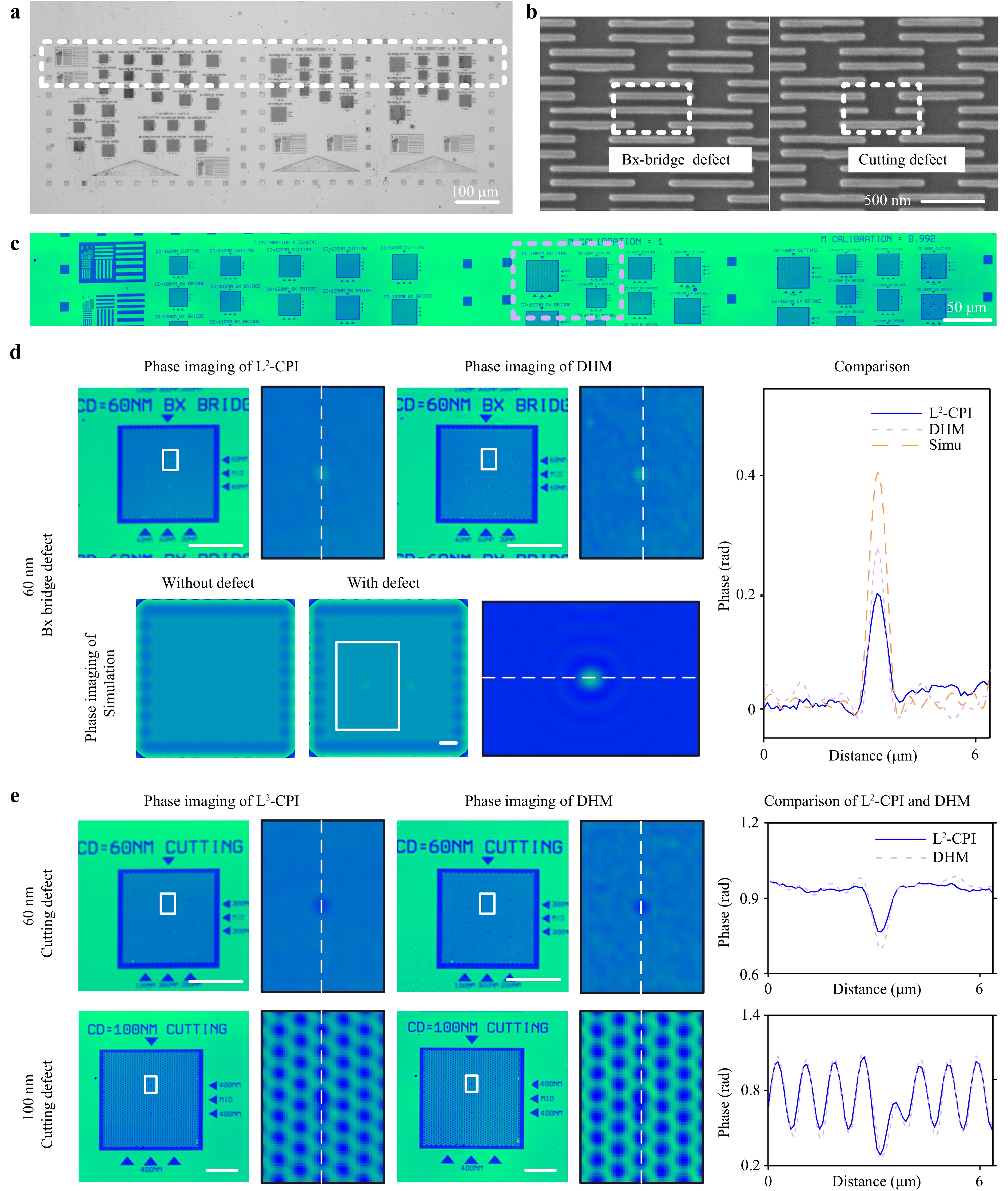
Fig. 4 Patterned wafer defect inspection based on L2-CPI. a The bright-field microscopic image of the patterned area and the L2-CPI-measured region (encircled by a white dashed box) on the IDA wafer. b The SEM images of a bridge defect and a cutting defect. c The reconstructed phase map of the selected area using L2-CPI, where the purple region containing IDA is used for comparison. d The reconstructed phase maps for the bx-bridge defect area using L2-CPI and DHM, along with the simulated phase maps for a bx-bridge defect of the same size. Experimental phase map scale bar: 10 µm, simulated phase map scale bar: 1 µm. e The reconstructed phase maps for the cutting defect areas using L2-CPI and DHM. Scale bar: 10 µm.
-
In summary, we developed a new computational phase imaging architecture called L2-CPI for the nondestructive computational phase imaging of transparent and opaque samples without compromising FOV and optical resolution. Unlike conventional phase imaging systems, which rely on multi-step measurements and image stitching for large-scale samples, L2-CPI could achieve the high-resolution imaging of an arbitrarily large sample in a single consecutive scanning process. We experimentally validated the high resolution (diffraction-limited, which is the same as that of conventional QPI techniques), the height-measurement accuracy (< 1 nm in comparison with the golden standard DHM), the robustness (noise reduction by more than 70% compared to the conventional QPI techniques in a dynamic imaging mode), and the ultra-large FOV (theoretically arbitrary large, limited only by the travel range of the sample stage in a single consecutive scanning process) of L2-CPI, by imaging both transparent and opaque samples. We hope the proposed L2-CPI can open a new direction for large-scale, fast, and high-resolution phase imaging, which may find applications in diverse fields such as nanosensing, bioimaging, material characterization, microelectronics testing, and semiconductor inspection.
-
We validate the concept of L2-CPI through an in-house developed epi-illumination interference microscope, which consists of an illumination module and an interferometer module. The illumination module has a 532 nm single longitudinal-mode laser (MSL-U-532, CNI Inc.). A rotating diffuser is used as a laser-speckle reducer after the light source. The diffuser is a 600-grit ground glass diffuser (DG10-600, Thorlabs Inc.), and the motor driving the diffuser rotates at 8,000 revolutions per minute. An objective (LMPLFLN 20X, Olympus Inc.) is used to couple light passing through the rotating diffuser into a multimode optical fiber (MMC600L-0.37-PC-1, Lbtek Inc.). A polarizer and a half-wave plate control the polarization direction of the collimated light exiting the multimode optical fiber. The illumination module can provide uniform and stable illumination for L2-CPI. The interferometer module is equipped with two identical objectives (LMPLFLN 100X, Olympus Inc.). Two cameras, i.e., one camera (ME2P-1843-21U3M, DAHENG IMAGING Inc.) operates in an area-array mode for the interferometer module. At the same time, the other (GT1930, Allied Vision Inc.) works in a linear-array mode for the dynamic compensation module in the DCS. The area-array camera is specially designed with the cover glass removed from its CMOS chip surface to prevent Newton’s rings caused by high-coherence illumination. Notably, the linear-array camera is essentially an area-array camera operating in a reduced linear-array mode, with a resolution of 1,936 (X-direction) × 1,216 (Y-direction) and a maximum full-frame rate of 50.8 FPS. When configured in a non-full frame mode (i.e., the linear-array mode we utilize), the resolution decreases to 1,936 × 200, enabling a frame rate of up to 76.8 FPS. A beam splitter divides the light into two beams for the two optical paths. A reference mirror is mounted on a PZT stage (PS1H30-015U-S, NanoMotions Inc.), which acts as the actuator in the DCS for axial compensation. This PZT stage has a maximum travel range of 15 µm and a resolution of 0.1 nm. When paired with a high-voltage controller (PCS211S, NanoMotions Inc.), its maximum response time is 20 ms, and its open-loop control frequency is 50 Hz. A motorized three-axis stage (PT1/M-Z8, Thorlabs Inc.) with a maximum speed of 3.3 mm/s is used for lateral scanning of the sample. The reference mirror and the sample are placed on the objectives’ focal planes, indicating that the interference fringes are straight. The reflective beams from the sample and the reference mirror pass through the same beam splitter and then enter the tube lens. After this, the combined beam is split by another beam splitter and captured by two cameras. The sample and the reference mirror are conjugated with the two cameras.
-
We employed electron beam lithography (EBL) to fabricate nanostructured silicon samples. A single-crystal silicon wafer with a thickness of 500 micrometers was selected as the substrate. The electron beam resist (AR-P 6200.09) was spin-coated onto the substrate, resulting in a photoresist film approximately 180 nm thick. Then, the IDA pattern was exposed onto the resist layer using the Vistec EBPG 5000plus ES electron beam exposure system at an energy level of 100 keV. The developed resist was immersed in Methyl Isobutyl Ketone (MIBK) solution for 70 seconds, followed by an Isopropanol (IPA) fixation process for 30 seconds. The residual isopropanol was evaporated using a hot plate set to 90 degrees Celsius. A PlasmaPro 100 Cobra Inductively Coupled Plasma (ICP) Etching System employing SF6 and C4F8 gases was then utilized for etching, which lasted 12 seconds. Finally, residual resist on the top of the nanostructures was removed using an oxygen plasma remover (Diener PICO). A stylus profiler characterized the etching depth, yielding a depth of approximately 140 nm.
-
This work was funded by the National Nature Science Foundation of China (Grant No. 52175509 and 52450158), the National Key Research and Development Program of China (2023YFF1500900), the Shenzhen Fundamental Research Program (JCYJ20220818100412027), Shenzhen Science and Technology Program (SGDX20230116093543005), and the Innovation Project of Optics Valley Laboratory (Grant No. OVL2023PY003). Thanks engineers Pan Li in Optoelectronic Micro&Nano Fabrication and Characterizing Facility, Wuhan National Laboratory for Optoelectronics of Huazhong University of Science and Technology for the support in device fabrication.
L2-CPI: high-resolution computational phase imaging with an arbitrary field of view
- Light: Advanced Manufacturing , Article number: 20 (2026)
- Received: 09 March 2025
- Revised: 23 December 2025
- Accepted: 03 January 2026 Published online: 05 June 2026
doi: https://doi.org/10.37188/lam.2026.020
Abstract: Optical phase imaging is a powerful tool widely used in bioimaging, material characterization, pathology, and nanomanufacturing. Yet, it faces a persistent challenge: the inherent contradiction between resolution and field of view (FOV) in conventional microscope-based systems. To address this limitation, we propose Lateral Line-Scan Computational Phase Imaging (L2-CPI), a novel computational phase imaging architecture that enables consecutive phase imaging of moving samples. Our experiments with both transparent and opaque samples demonstrate that L2-CPI achieves an equivalent FOV of D × L, where D is the camera sensor edge length and L is the motorized stage travel range. This implies that the equivalent FOV of L2-CPI in a single measurement can be arbitrarily large, provided the stage travel range L is arbitrarily long. Our work breaks the long-term contradiction between resolution and FOV, establishing a new paradigm for ultra-large-FOV phase imaging in dynamic mode without sacrificing optical resolution. This advancement holds significant potential for applications in bioimaging, material characterization, biosensing, nanometrology, and semiconductor inspection.
Research Summary
L2-CPI: Breaking the resolution–field-of-view trade-off in phase imaging
A new computational phase imaging technique enables high-resolution, label-free visualization of arbitrarily large samples in a single continuous scan. Conventional quantitative phase imaging systems are fundamentally limited by the inverse relationship between optical resolution and field of view (FOV). Jinlong Zhu, Liang Gao, Shiyuan Liu and colleagues at Huazhong University of Science and Technology introduce Lateral Line-scan Computational Phase Imaging (L2-CPI), which achieves diffraction-limited resolution and effectively unlimited FOV by fusing lateral scanning with phase imaging. L2-CPI successfully achieves reflection-mode, large-FOV phase imaging for both transparent and opaque samples. Demonstrated on an intentional defect array wafer, L2-CPI detects sub-60 nm defects during motion. It eliminates the resolution–FOV trade-off, enabling high-speed, stitch-free imaging for semiconductor inspection, bioimaging, and nanometrology.
Rights and permissions
Open Access This article is licensed under a Creative Commons Attribution 4.0 International License, which permits use, sharing, adaptation, distribution and reproduction in any medium or format, as long as you give appropriate credit to the original author(s) and the source, provide a link to the Creative Commons license, and indicate if changes were made. The images or other third party material in this article are included in the article′s Creative Commons license, unless indicated otherwise in a credit line to the material. If material is not included in the article′s Creative Commons license and your intended use is not permitted by statutory regulation or exceeds the permitted use, you will need to obtain permission directly from the copyright holder. To view a copy of this license, visit http://creativecommons.org/licenses/by/4.0/.

 DownLoad: