


-
Refractive index (RI) sensing in the mid-infrared (MIR, 2.5–25 μm) spectral window has emerged as a powerful analytical tool, leveraging the unique absorption signatures of molecular bonds for selective detection of chemical and biological species1–3. Metasurfaces—artificial subwavelength nanostructures—offer unprecedented opportunities to enhance light-matter interaction through tailored resonance engineering4–6. However, conventional MIR metasurfaces predominantly rely on two-dimensional (2D) plasmonic designs fabricated via electron-beam lithography (EBL) or focused ion beam (FIB) milling, which suffer from high fabrication costs, limited scalability, and residual contamination caused by polymeric resists. Recent advances in three-dimensional (3D) metasurfaces, featuring vertically modulated nanostructures with submicron height variations, have shown promise for boosting sensing performance by combining the field-enhancement benefits of 3D architectures with the fabrication simplicity of planar systems7,8. As one of the most mainstream 3D micro/nanofabrication methods, two-photon polymerization (TPP) has garnered widespread attention for its flexible 3D structure construction capabilities9. However, when fabricating plasmonic metasurfaces, this approach requires coating the fabricated 3D substrate with a continuous metal film, making it difficult to construct periodic discrete metallic structures, which are crucial to realize localized surface plasmon resonance10–12. This reduces the degree of freedom in the structural design for TPP fabricated metasurfaces. Alternatively, ion beam-induced folding can also create 3D metasurfaces, yet questions remain regarding their structural integrity and practical application performance13,14.
Ice lithography (also known as ice-assisted electron beam lithography), a cryogenic patterning technique using ice as a resist, presents a solvent-free alternative for nanoscale fabrication with the minimum feature size as small as 4 nanometers15–17. By eliminating organic resists and development solvents, it enables residue-free surfaces critical for maintaining high plasmonic resonance quality. This clean, solvent-free process is also highly desirable for biosensing, as it minimizes the risk of chemical contamination that could interfere with biological analytes18,19. Leveraging the relatively low sensitivity of amorphous water ice to electron beams, this technique allows for in-situ scanning electron microscopy (SEM) imaging observation at multiple stages of the patterning process, enabling precise in-situ alignment overlay19,20. Consequently, complex 3D geometries can be efficiently fabricated using multilayer exposure processes. Furthermore, ice layers can uniformly condense and form films on cryogenic substrates of virtually any shape, thereby enabling ice lithography-based nanofabrication to transcend the limitations of planar substrates. Currently, from a materials perspective, ice lithography-based 3D structure fabrication has encompassed metals, carbon-based organic molecules, and metal-organic compounds19–24. Regarding substrate compatibility, ice lithography has successfully patterned micro/nano structures on diverse non-planar surfaces, including atomic force microscope (AFM) tips, fiber sidewalls, and fiber end faces16,20. It has been shown in several recent works that ice lithography can be directly performed even on biological substrates such as biological membrane and living tardigrade surfaces (such patterning has so far remained limited to the use of organic ice resists due to challenges such as the susceptibility of biological organisms to damage when using water ice resist)25,26. Consequently, ice lithography-based 3D fabrication demonstrates significant application potential in fields such as biosensing, flexible electronics, and fiber-optic communications.
Despite its advantages, ice lithography remains underexplored for MIR metasurfaces, particularly for complex 3D geometries. Here, we harness ice lithography’s unique capabilities—including solvent-free processing, in situ alignment, and multilayer stacking in a unified vacuum system—to fabricate a 2.5-dimensional (2.5D) gold cross-pillar metasurface. Simulations confirm that pillar height tunes plasmonic resonant wavelength and near-field confinement, while experimental validation demonstrates significantly enhanced RI sensitivity with a high quality factor (high-Q). This work bridges nanofabrication sustainability with high-performance sensing, paving the way for future advances in on-chip photonics for molecular fingerprint detection.
-
The proposed 2.5D plasmonic metasurface, illustrated in Fig. 1, features a unit cell composed of a gold cross (arm dimensions: length l, width w, height h1) with four vertically oriented square pillars (width w, height h2) positioned at its endpoints. We term this architecture ‘2.5D’ Dash referring to metasurfaces with vertically discrete, subwavelength-scaled topography (e.g., pillars or steps) fabricated via planar-compatible processes. Unlike full 3D nanostructures requiring complex processing techniques, 2.5D designs maintain the fabrication scalability of 2D systems while enabling tailored field confinement along the z-axis for enhanced light-matter interaction. This architecture is fabricated on a layered substrate consisting of a SiO2 insulation layer (thickness t1), a gold back-reflector (thickness t2), and a 500 μm intrinsic silicon handle wafer. The entire structure adopts the metal-insulator-metal (MIM) configuration27,28, with a unit period of Px=Py=2 400 nm. Other structural parameters here were set as l=2 000 nm, w=200 nm, h1=100 nm, t1=200 nm and t2=100 nm, respectively, with h2 ranging from 0 to 800 nm. The design strategically exploits vertically expanded plasmonic modes to enhance near-field confinement at pillar-crown interfaces, which serve as primary analyte-binding sites.
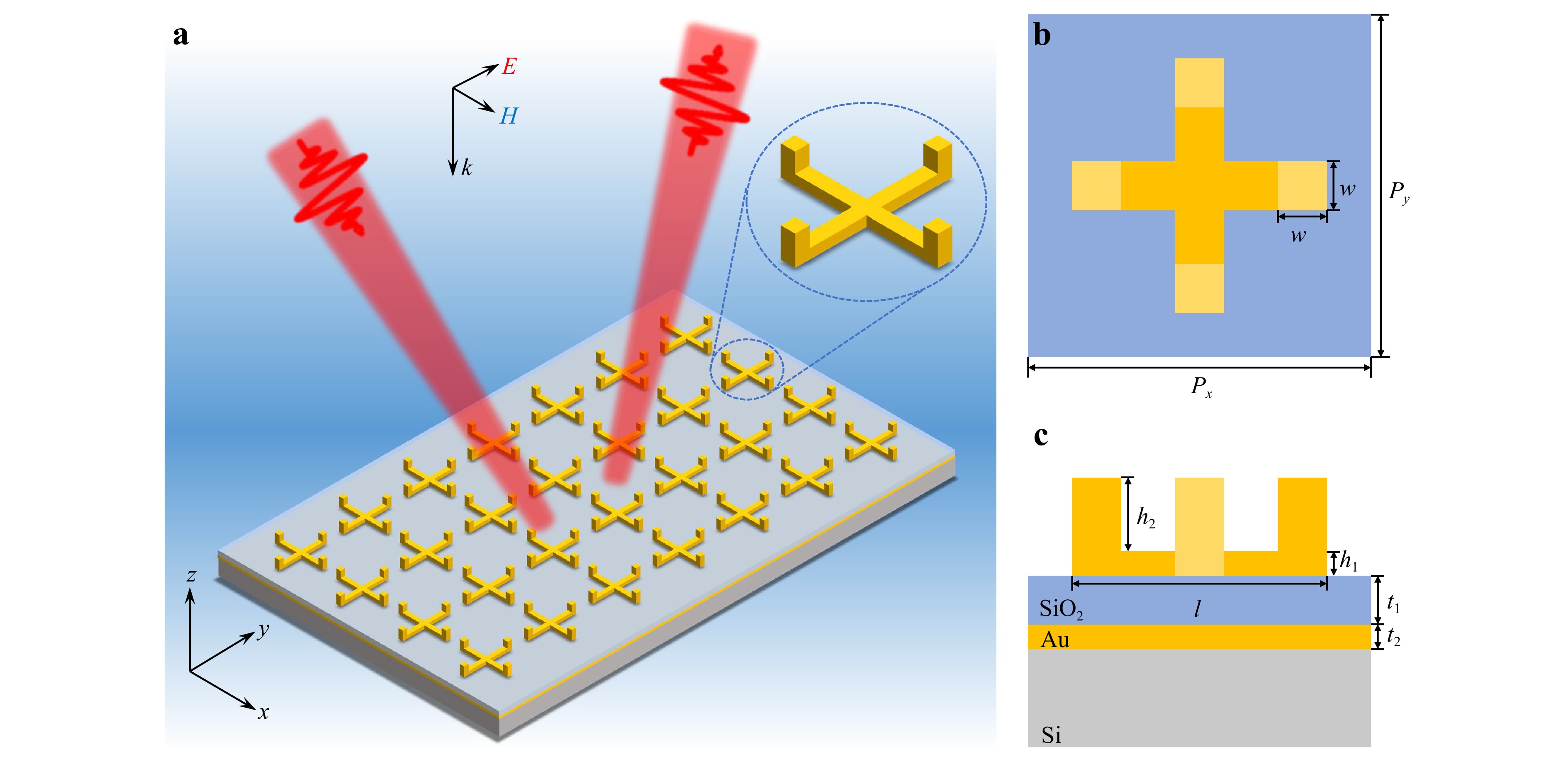
Fig. 1 a Schematic diagram of the designed 2.5D plasmonic metasurface, with blue dashed lines outlining the unit structure illustration. b Top view and c side view of the metasurface unit structure with dimensional labeling.
Similar structures termed as four-tined fish-spear-like resonators (FFRs) have been fabricated by TPP 3D printing, which constitutes a continuous metal plane on the surface, with adjacent resonators short-connected via a thin metal film10. Consequently, localized plasmonic resonance could only be achieved by increasing the structure’s aspect ratio, and such plasmonic structures were limited to reflective operation10,13. Compared to the TPP method, ice lithography offers significantly higher fabrication precision, enabling the extension of the resonance wavelength into the near-infrared (NIR) and visible bands. Additionally, the resonators can be configured as either shorted or isolated, making the structure compatible with both transmission and reflection operational modes.
Fabrication of this intricate 2.5D geometry was achieved through a customized in situ ice lithography process. Fig. 2a-g shows the entire ice lithography fabrication process through schematic diagrams and corresponding in-situ SEM images. Specifically, after the substrate is cooled to the target temperature within the ice lithography system, it undergoes two cycles of 'ice formation → electron beam exposure → metal deposition' (Fig. 2a-f). The sample is then warmed and purged with nitrogen gas to blow off excess metal, yielding the final device (Fig. 2g). This demonstrates that the system and process enable ‘wafer in, device out’ capability within a single loading/unloading sequence. Unlike conventional EBL, which relies on polymer resists (e.g., polymethyl methacrylate, PMMA) requiring toxic solvents for spin-coating and development, this method utilized amorphous water ice as a sacrificial resist. SEM images in Fig. 2g, h and the 3D AFM image in Fig. 2h further verified favorable surface roughness and near-vertical pillar profiles, minimizing optical scattering losses—a common limitation in FIB/plasma-etched metasurfaces.
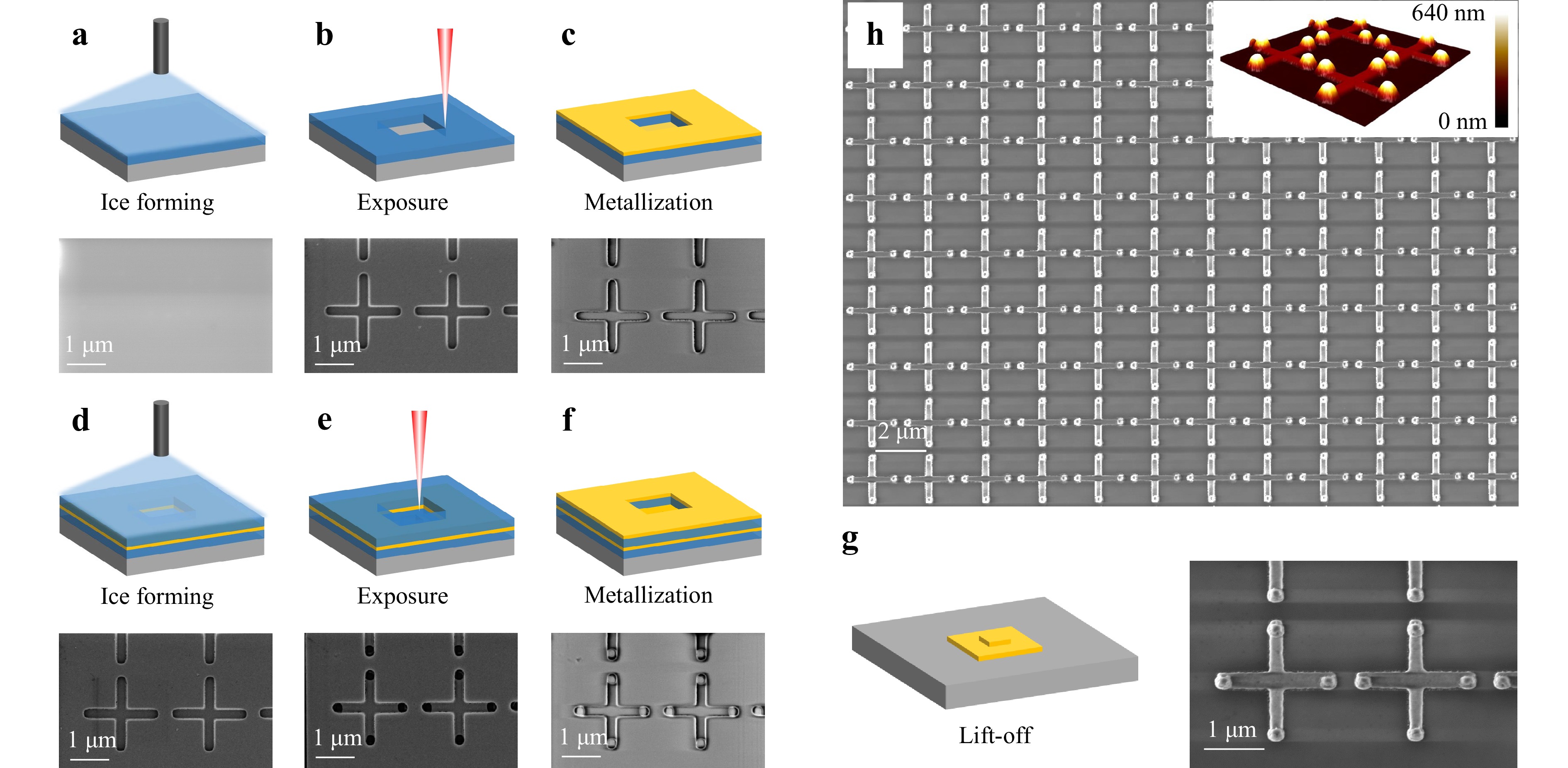
Fig. 2 a-g Process flow diagram of ice lithography for 2.5D metasurfaces with corresponding in-situ SEM images at every stage. h Overall SEM image of the 2.5D metasurface with the upper-right inset showing a 3D topographical image of a local region of the metasurface obtained by AFM scanning.
Ice lithography offers three transformative advantages. The first one is eco-compatibility and substrate versatility: The absence of organic chemicals (resists, developers, strippers) renders the process inherently clean and low-toxicity. Ice’s conformal deposition on nonplanar or fragile substrates (e.g., perovskite29,30, 2D materials31,32, and even living animals26) was critical for achieving uniform multilayer patterning without mechanical stress. The second advantage is nanoscale alignment precision: Leveraging the low sensitivity of amorphous ice to electron beams, we can perform in situ SEM imaging after each lithographic cycle (Fig. 2a-g). This enabled real-time alignment correction. The SEM image in the right panel of Fig. 2g, as well as the tilted SEM view in Fig. S2, confirms successful stacking of the cross (h1=100 nm) and pillar (h2=300 nm) layers with high precision. The third advantage is multilayer processing efficiency: Although ice requires a higher exposure dose (~0.8 C/cm2 at 5 keV for 600 nm thick water ice) compared to PMMA (typically ~100 μC/cm2), the unified vacuum workflow (ice formation → electron beam exposure → metal deposition) eliminated sample transfer between tools. For N-layer structures, this reduced total steps by 3N+1, making ice lithography increasingly efficient for small scale complex 3D devices.
To characterize the optical response of this metasurface in the mid-infrared (MIR) band, we simulated the reflection spectrum of the device. As shown in Fig. 1a, linearly polarized light is incident along the negative z-direction, normal to the metasurface plane, with its electric field parallel to the x-axis. It is important to note that due to the designed C4 symmetry of the metasurface, its optical response is therefore polarization-insensitive. The reflection spectrum as a function of h2 is shown in Fig. 3a. For the planar metasurface (h2=0 nm), a reflection dip can be observed at about 5.7 μm. With the increase of h2, the spectrum exhibits a linear redshift to around 8.1 μm for h2=1 000 nm. Throughout this variation, the Q factor remains almost constant or even slightly increases, reaching its maximum value of approximately 20 at h2=700 nm. The shape of the reflection curve in Fig. 3a shows minimal change with h2, indicating that the type of resonance remains unaltered. This observation is further corroborated by the electric field distributions and the results of multipole analysis shown in Fig. 3b-e. We selected the cases of h2=0 nm and h2=300 nm as representative planar and 2.5D metasurface structures, respectively, and performed simulation analysis on them. Comparing the multipole analysis results in Fig. 3d, e reveals that the resonance in both structures is predominantly governed by the electric dipole (ED) mode, accounting for over 95% of the contribution at the resonance center (see Fig. S3).
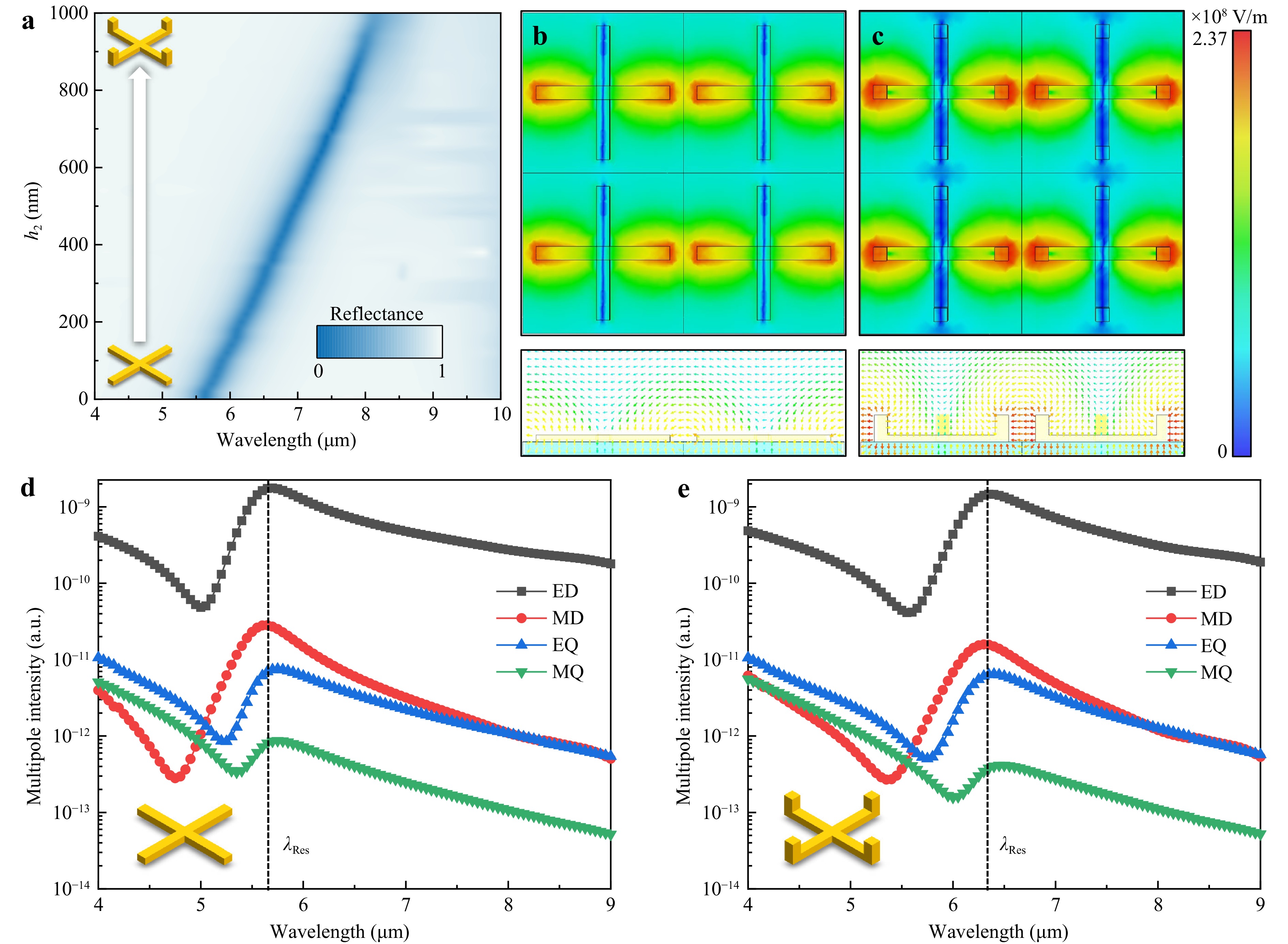
Fig. 3 a The simulated reflectance spectra as a function of the pillar height h2. b, c Electric field intensities and vectors (arrows) at resonant wavelengths (λRes) for the planar (h2=0 nm) and 2.5D (h2=300 nm) plasmonic metasurfaces, respectively. d, e Dispersion of radiation power for various multipole moments induced in the planar (h2=0 nm) and 2.5D (h2=300 nm) plasmonic metasurfaces, respectively.
To elucidate the role of vertical topology in RI sensing performance, the metasurface’s sensing capability was quantified by simulating resonance shifts under varying ambient refractive indices (n=1.0–1.5) as shown in Fig. 4a-c. Fig. 4a, b present the reflection spectra versus environmental RI for the cases of h2=0 nm and h2=300 nm, respectively. Both cases exhibit nearly linear resonance shifts in response to changes in the environmental RI. It can be observed that the magnitude of the resonance shift is significantly larger for h2=300 nm compared to h2=0 nm. Simulation results for the resonance shifts across various heights are summarized in Fig. 4c, where linear fitting was performed on each dataset. The sensing sensitivity S, calculated from the slope of the linear fit, gradually increases with rising h2. The corresponding sensitivity values S (defined as the resonance shift per unit change in the refractive index of the surrounding environment) for h2=0, 100, 200, 300, 400, 500, and 800 nm are 1 980 nanometers per refractive index unit (nm/RIU), 2 480, 2 755, 2 940, 3 019, 3 265, and 4 208 nm/RIU, respectively. Given that the Q-factor of the metasurface remains largely constant across the h2 range of 0–800 nm, the enhancement in S directly leads to a notable improvement in the figure of merit (FOM).
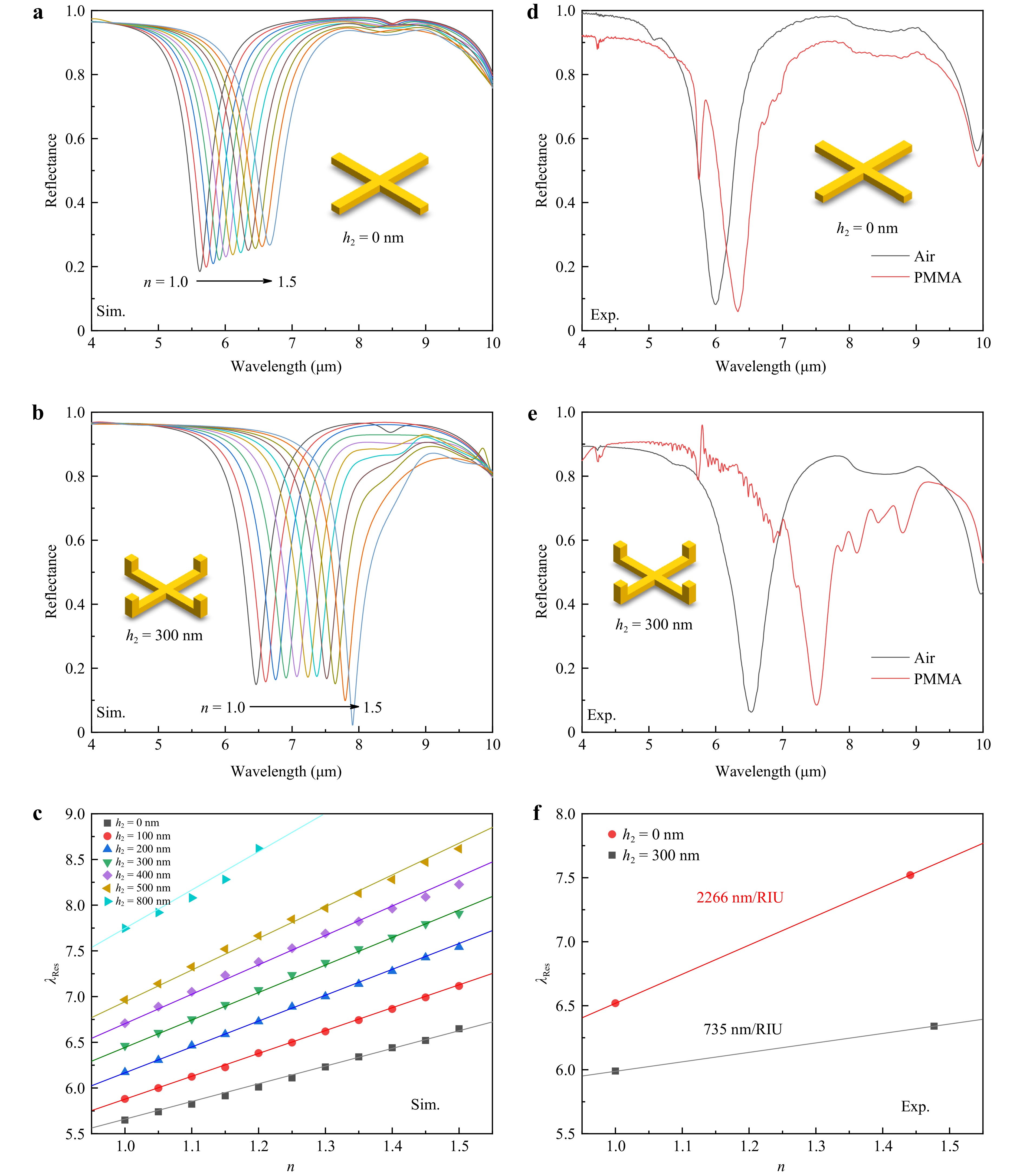
Fig. 4 a, b Simulated reflection spectra with ambient refractive indices ranging from 1.0 to 1.5 for the planar (h2=0 nm) and 2.5D (h2=300 nm) plasmonic metasurfaces respectively. c Simulated dependence of resonant wavelengths (λRes) on ambient refractive index with h2 varying from 0 to 800 nm and linear fitting. d, e Experimentally measured reflection spectra of the metasurface-based sensor across different dielectric media for the planar (h2=0 nm) and 2.5D (h2=300 nm) plasmonic metasurfaces, respectively. f Experimental dependence of resonant wavelengths (λRes) on ambient refractive index with h2=0 nm and 300 nm and linear fitting.
On the other hand, more simulation results in Fig. S4 indicate that for h2≥400 nm, the full width at half maximum (FWHM) of the resonance dip broadens significantly at higher n values, leading to a noticeable decrease in the Q-factor. This degradation becomes more pronounced with increasing h2, which would adversely affect the FOM in sensing applications where n is high (n˃1.4 for h2=300 nm; n˃1.2 for h2=600 nm; n˃1.1 for h2=800 nm). In contrast, for structures with h2≤300 nm, the Q-factor remains remarkably stable across the refractive index range from n=1.0 to n=1.5. Therefore, while taller pillars offer higher absolute sensitivity, the h2=0–300 nm range provides a more consistent and reliable FOM over a broader effective sensing range, making it more suitable for practical applications.
Experimentally, we fabricated devices with h2=0 nm and 300 nm and measured reflectance spectra in different dielectric environments: air (n=1.0) and PMMA (the dispersive refractive index information of PMMA was obtained from Ref. 37), as depicted in Fig. 4c, d. The resonance red-shifted by about 1 000 nm in PMMA, yielding a sensitivity of 2 266 nm/RIU. This represents a 3.1-fold enhancement over planar control devices (735 nm/RIU from experiment), validating our pillar-enhanced sensing mechanism. The discrepancy versus simulations is attributed to edge roughness and minor deviations in material properties and fabrication tolerances, which slightly reduce field homogeneity and degrade the sensing performance. The fabricated metasurface devices underwent multiple cycles of PMMA spin-coating, baking at 180°C, immersion in organic solvents, nitrogen purging, plasma cleaning, and brief sonication (up to 1 minute in most cases). The structures remained intact throughout these processes, and the spectral measurements showed excellent consistency, thereby demonstrating remarkable device stability. It should be noted that extended sonication (e.g., > 3 minutes) risks delaminating both the metasurface and the SiO2 layer.
Compared with those of plasmonic infrared sensors reported recent years, the sensitivity in this work (2 940 nm/RIU in simulation and 2 266 nm/RIU in experiment) represents a high value11,33–35. Only Ref. 11 showed the higher simulated result of 6 400 nm/RIU. Our measured Q-factor of around 20 is also higher than that of most reported works. In terms of structure and fabrication methodology, most of the reported metasurfaces consist of 2-3 structural layers, requiring multiple alignment steps and sample transfers between different instruments for processing. In contrast, our work is the only one completed within a single vacuum system in a single load/unload cycle, demonstrating the significant advantages of ice lithography in processing efficiency and in-situ alignment. However, it is important to note the limitations of the ice lithography method. The exposure dose required for water ice is relatively high (approximately 1 000 times that of PMMA of the same thickness), causing it to lose its efficiency advantage in scenarios requiring large-area electron beam exposure (e.g., millimeter to centimeter-scale devices). It is therefore more suitable for the fabrication of sub-millimeter scale and smaller devices. Furthermore, ice lithography is particularly well-suited for specialized scenarios such as fabrication on non-planar substrates, substrates requiring cryogenic protection, and structures demanding local and precise alignment.
To further understand the modulation mechanism of pillar height on sensing performance, it is imperative to correlate simulation results of electric field distributions and multipole components. This tunability arises from two synergistic effects. The first one is enhanced field-analyte overlap: Electric field distributions (Fig. 3b, c) demonstrate that pillars elevate the field maxima away from the substrate interface, exposing more energy to the ambient medium. Secondly, the results of multipole analysis (Fig. 3d, e and Fig. S3) confirmed that the resonance is dominated by an electric dipole (ED) contribution (> 95%). Taller pillars (h2=300 nm) intensified the ED moment by 3 times while suppressing other resonance modes, concentrating energy at pillar tips where analyte interaction is maximized. Vector plots (arrows in Fig. 3b, c) further visualize field lines penetrating the dielectric environment—directly enabling RI sensitivity.
Our pillar-height-dependent sensitivity enhancement employs similar geometric tuning strategies with recent works exploiting local-to-nonlocal transitions in plasmonic metasurfaces36. However, the optimization goals diverge: While reducing structural height suppresses dissipation loss to achieve ultrahigh Q-factors, it fixes resonance wavelengths near the lattice period (λ≈P), limiting refractive index tunability. Conversely, our design increases pillar height to extend the electric field into analytes, boosting sensitivity to 4 208 nm/RIU with the Q factor almost unchanged. This highlights a broader design principle: vertical topology controls light-analyte interaction channels, with height parameters dialing between sensitivity (field-analyte overlap) and Q-factor.
-
In summary, this work theoretically and experimentally demonstrates a high-performance MIR refractive index sensor using ice-lithographed 2.5D plasmonic metasurfaces. The strategic manipulation of 2.5D pillar height in asymmetric gold cross-pillar architectures directly enhances refractive index sensitivity by concentrating electric fields at analyte-accessible sites, achieving a 3.1-fold experimental sensitivity boost (2 266 nm/RIU) and up to 4 208 nm/RIU in simulations. In this work, ice lithography unlocks unique technological advantages—including solvent-free multilayer stacking, high-precision in situ alignment, and conformal processing on unconventional substrates—to enable residue-free fabrication of high-performance sensors. This synergy between vertically engineered plasmonics and solvent-free nanofabrication establishes a versatile platform for next-generation 3D metasurfaces/metamaterials, particularly for (bio)chemical sensing based on molecular fingerprint detection in the MIR region.
-
First, a 10-nm-thick Ti film and a 100-nm-thick Au film were sputter-deposited onto a 500-μm-thick intrinsic polished Si(100) wafer. This was followed by the growth of a 200-nm-thick SiO2 film using plasma-enhanced chemical vapor deposition (PECVD). Next, an ice lithography cycle was performed on the resulting substrate using a Zeiss Sigma 300 SEM equipped with a liquid nitrogen dewar, a cryogenic stage, and a thermal evaporation system. The specific steps of ice-lithography are illustrated in Fig. 2a-g. The substrate was cooled from room temperature to approximately 130 K over a period of 2-3 hours, as monitored by a PT100 platinum resistor mounted on the sample stage. Maintaining a temperature below 135 K was critical, as higher temperatures resulted in rough ice films that were unsuitable for exposure. The ice deposition rate, which is proportional to the pressure drop rate in the gas injection system (GIS), was controlled by a needle valve to maintain a rate of ~4 mTorr/s, with the pressure being tracked in real-time by a Pirani gauge (INFICON CDG 025D). The total thickness of the ice layer was calibrated against the total pressure drop in the GIS. For the specific 2.5D metasurface device fabrication, the total pressure drops for the first and second ice layers were set at 300 mTorr and 700 mTorr, respectively. All exposures were performed with a 10 kV electron beam acceleration voltage. Next, a metal layer was deposited via physical vapor deposition (PVD) at a rate of 0.3−0.5 Å/s. After processing, the sample was returned to room temperature and removed from the SEM chamber. Finally, gentle nitrogen blow-off at a pressure ranging from 25−40 psi was applied for several seconds to remove the redundant wrinkled gold film, yielding the final 2.5D metasurface device.
-
The reflection spectrum and surface electric field distribution of the metasurface were simulated using finite difference time domain method, while multipole decomposition analysis was conducted by finite element method. Periodic boundary conditions were applied in the x and y directions, while perfectly matched layers were set as the top and bottom boundaries.
-
The surface morphology of the device structure is characterized with a Zeiss Sigma 300 scanning electron microscope and a Bruker Dimension ICON Bruker atomic force microscope. The reflectance spectra were measured with a Bruker Vertex 80v Fourier transform infrared spectrometer coupled with a Hyperion 3 000 infrared microscope using a ×36 objective lens. To verify the environmental refractive index sensing performance of the metasurface, a 400 nm-thick PMMA film was spin-coated onto the device surface and baked at 180°C for 1 minute prior to testing. The dispersive refractive index information of PMMA was obtained from Ref 37.
-
This work was supported by the National Key Research and Development Program of China (No. 2024YFB2809200), the National Natural Science Foundation of China (52203305 and U21A20494), the National Key Laboratory of Laser Spatial Information Foundation (LSI2025WDZC12) and the Key Project of Westlake Institute for Optoelectronics (2023GD008).
Refractive index sensing in the mid-infrared regime with ice-lithography enabled 2.5-dimensional metasurfaces
- Light: Advanced Manufacturing , Article number: 29 (2026)
- Received: 24 July 2025
- Revised: 16 January 2026
- Accepted: 25 January 2026 Published online: 03 March 2026
doi: https://doi.org/10.37188/lam.2026.029
Abstract: Mid-infrared (MIR) refractive index (RI) sensing holds significant potential for applications in chemical detection, environmental monitoring, and biomedical diagnostics due to the strong molecular vibrational fingerprints in this spectral range. However, conventional metasurface-based sensors face challenges in fabrication complexity, toxic solvents, and performance optimization. Here, we introduce ice-lithographed 2.5-dimensional (2.5D) plasmonic metasurfaces featuring vertically asymmetric gold cross-pillar resonators to overcome these challenges. The solvent-free ice lithography enables in situ scanning electron microscopy (SEM) alignment with high precision, residue-free surfaces, and multilayer stacking in a single vacuum process. Simulations reveal that vertically graded pillars (height 0–800 nm) linearly redshift resonance wavelengths while concentrating electric fields at analyte-binding sites, boosting experimentally measured sensitivity from 735 nanometers per refractive index unit (nm/RIU) to 2 266 nm/RIU. This work demonstrates a three-dimensional (3D) architectural strategy for enhancing sensing performance, while simultaneously unveiling the potential of ice lithography in fabricating low-toxicity and flexible 2.5D sensing devices.
Research Summary
Ice-lithographed 2.5D Plasmonic Metasurfaces Boost Refractive Index Sensing Sensitivity
Mid-infrared (MIR) refractive index (RI) sensing is vital for chemical, environmental and biomedical applications, but conventional metasurface sensors face fabrication complexity and toxicity issues. Researchers report ice-lithographed 2.5D plasmonic metasurfaces with asymmetric gold cross-pillar resonators. Solvent-free ice lithography enables in-situ SEM alignment, residue-free surfaces and single-vacuum multilayer stacking. Simulations show vertically graded pillars linearly redshift resonance wavelengths and concentrate electric fields at analyte sites, while experiments boost sensitivity from 735 to 2266 nm/RIU, unlocking low-toxicity, high-performance devices for MIR molecular fingerprint detection.
Rights and permissions
Open Access This article is licensed under a Creative Commons Attribution 4.0 International License, which permits use, sharing, adaptation, distribution and reproduction in any medium or format, as long as you give appropriate credit to the original author(s) and the source, provide a link to the Creative Commons license, and indicate if changes were made. The images or other third party material in this article are included in the article′s Creative Commons license, unless indicated otherwise in a credit line to the material. If material is not included in the article′s Creative Commons license and your intended use is not permitted by statutory regulation or exceeds the permitted use, you will need to obtain permission directly from the copyright holder. To view a copy of this license, visit http://creativecommons.org/licenses/by/4.0/.

 DownLoad: