






-
Transition metal dichalcogenides (TMDCs) have recently emerged as prospective alternatives to traditional semiconductors for photonic applications in the visible and infrared (IR) spectral regions1–6. These ultrathin semiconductors possess high refractive indices5,7–10, optical non-linearity11–13, and optical anisotropy9,14,15, making them attractive for photonic applications. These properties, along with the large optical path lengths relative to their atomic-scale thicknesses2, suggest the potential of TMDCs for fabrication of miniature photonic structures with low surface/volume losses2,4 compared with traditional photonic semiconductors and metals4. Diffractive optical elements1,2,11, in particular, enable precise control of the propagation and phase of light, making them essential components for realising compact and multi-functional photonic devices16.
However, the practical implementation of TMDCs in photonics remains largely restricted by constraints in the fabrication of micro and nanostructures with well-defined geometries. Previous studies on the fabrication of diffractive and refractive miniaturised photonic structures2,11,17 relied on the use of single-crystal flakes in conjunction with microstructuring methods such as focused ion beam (FIB) milling. Although these methods2,11,17 successfully demonstrate the underlying concept, they are time-consuming and likely prone to introduce phase errors in diffractive optical elements, which can compromise their efficiency. This stems from positioning inaccuracies, as the FIB can only process a small area at a time, the size of which depends on the resolution of the patterning, and therefore, stitching of adjacent structures is required to cover larger areas. The limited flake size (typically several micrometres) and processing area of FIB restrict scalability, and hence, there is a critical need for more flexible manufacturing approaches6. Therefore, to fulfil the requirements for the practical implementation of these materials beyond the experimental realm, scalable synthesis and manufacturing methods should be devised.
Recent developments in the synthesis of TMDCs have shown that various precursors can be locally decomposed by laser irradiation in the visible and ultraviolet (UV) spectral ranges to produce MoS2, WS2, their alloys, as well as tin sulfides18–21. Notably, these studies18–21 have shown that non-irradiated precursor materials can be selectively removed by solvents, enabling a photolithographic process and thereby achieving micro/nanostructuring of the resultant TMDCs during their synthesis. However, direct laser synthesis requires a relatively high-intensity illumination, which leads to chemical and structural inhomogeneities that may limit precision patterning18,20.
In this study, we exploited the selective solubility characteristics of Mo and W thiosalts ((NH4)2MoS4 and (NH4)2WS4)18–20, which served as chemical precursors for MoS2 and WS2, to fabricate diffractive optical elements on various photonic platforms, including SiO2 and LiNbO3. This approach hinges on the chemical aspect of the precursors18,22,23, which allows the production of intermediate amorphous chemical products using lower-intensity laser irradiation, compared with direct synthesis. These intermediate amorphous chemical products can be post-processed to produce microstructured films of the desired TMDC. Unlike the pristine exfoliated micrometre-sized flakes, the resultant films were polycrystalline. However, if the optical response remains comparable to that of pristine films, they can be used to fabricate diffractive and other photonic structures. We produced 1D and 2D diffraction gratings with periods as short as 150 nm, and the Fresnel holograms were directly synthesised onto SiO2 and LiNbO3 substrates. The diffraction efficiency and spectroscopic ellipsometry measurements indicated that the refractive index of the material synthesised in this manner (pre-patterning followed by thermal annealing) was comparable to that measured in similar structures reported in the literature1,2,11,24–26 using pristine flakes. We demonstrated that the fabrication process operated across a wide range of irradiation conditions (laser intensities and wavelengths), indicating pronounced flexibility in the fabrication process.
-
The steps involved in laser synthesis to produce TMDCs are schematically illustrated in Fig. 1a. First, an Mo or W thiosalt precursor solution was spin-coated onto the substrate. After drying, the precursor film was irradiated using a visible/UV laser beam and finally the irradiated film was “developed” in an organic solvent (N-methyl-2-pyrrolidone (NMP)) to remove the unexposed precursor but leaving the film in the irradiated regions unaffected.
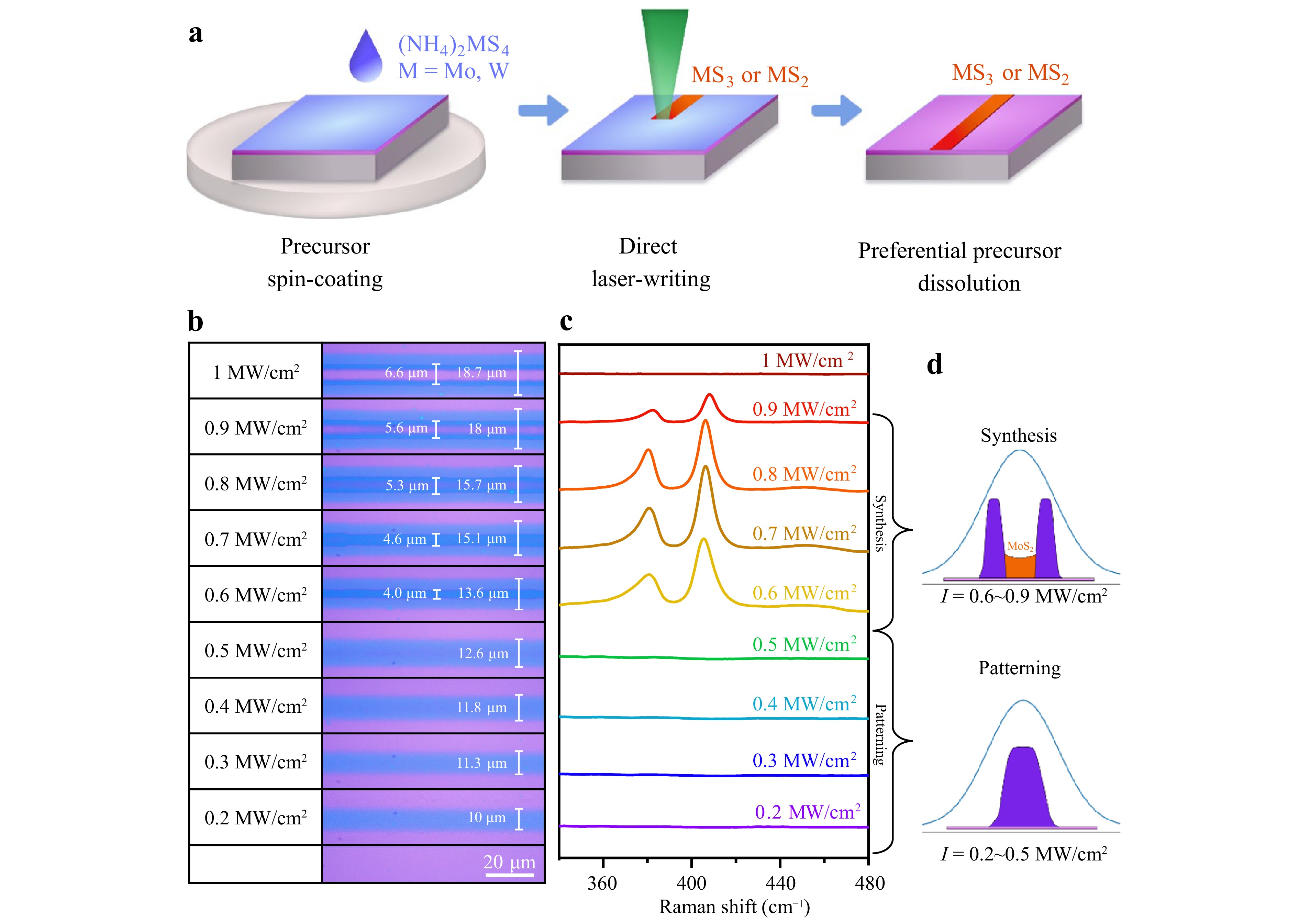
Fig. 1 a Schematic representation of the steps involved in the synthesis of MS2/MS3 (M = Mo, W) using (NH4)2MS4 precursor by direct laser irradiation: i) precursor solution preparation and spin-coating; ii) localised synthesis of MS3 or MS2 by laser irradiation; iii) preferential removal of the untreated precursor using organic solvents. b Optical images of tracks produced using (NH4)2MoS4 precursor, irradiated with a continuous wave laser at a wavelength of 532 nm at various peak intensities and c the corresponding Raman spectra. d Schematic representation of the resultant track morphology (cross section) owing to the i) Gaussian intensity profile (blue curve) and peak intensity of the beam. The top profile (0.6–0.9 MW/cm2) illustrates MoS2 synthesis in the central zone, whereas the bottom profile (0.2–0.5 MW/cm2) represents conditions leading to patterning of the amorphous material. The purple regions indicate amorphous material, whereas the orange region corresponds to MoS2.
Fig. 1b shows the developed tracks of the laser-irradiated (NH4)2MoS4 precursor film onto the SiO2/Si substrate at various laser intensities, as indicated on the left side of the figure. The corresponding Raman spectra for all irradiated tracks are shown in Fig. 1c. As the laser intensity increased, the characteristic in-plane E2g (383 cm−1) and out-of-plane A1g (408 cm−1) Raman modes became detectable at 0.6 MW/cm2 and persisted up to a laser intensity of 0.9 MW/cm2. These modes are associated with crystalline MoS227. As the laser intensity increased, the intensity of these Raman peaks started to decrease at 0.8 MW/cm2 and finally disappeared at 1 MW/cm2 as a consequence of laser-induced thinning28. The change in thickness at the centre of the tracks could be observed in the corresponding optical microscopy images shown in the same figure. At laser intensities between 0.2 and 0.5 MW/cm2, it was still possible to obtain "developed" tracks; however, they did not correspond to crystalline MoS2 as they did not exhibit the characteristic Raman peaks. The chemical composition of these irradiated areas rendered them resistant to dissolution in the "developing" chemical agents, thereby providing a negative-tone photolithographic function.
Thus, laser irradiation of thiosalt precursors can be used to i) produce an intermediate amorphous compound at low-intensity irradiation or ii) induce direct laser synthesis of TMDC. Finally, at higher-intensity extremes, laser thinning and removal of the synthesised material occurred. The associated topographies of the tracks are shown in Fig. 1d. The top cross section illustrates the profile formed under laser intensities of 0.6–0.9 MW/cm2. At these high peak intensities, MoS2 synthesis occurred in the central region of the irradiated area. However, the side lobes consisted of an amorphous precursor material, owing to the Gaussian intensity distribution and corresponding temperature profile, which led to non-uniform heating across the irradiated spot. A linear Raman spectroscopy scan across the laser-synthesised track is shown in Fig. S1 of the Supplementary Material, in conjunction with the track physical dimensions, indicating a polycrystalline central region and amorphous side lobes. The atomic force microscopy (AFM) profile is also shown to indicate the height difference between the amorphous and polycrystalline regions. In contrast, the profile obtained under lower laser intensities, below the direct synthesis threshold, showed an exclusively amorphous material with a more uniform morphology. It is evident that there was a volume change between the side lobes consisting of amorphous material and the central region where the synthesis of the TMDC had occurred. The AFM measurements suggested that this volume change was ~50%.
We analysed the material contained in these sub-threshold tracks using scanning transmission electron microscopy (STEM) and energy-dispersive X-ray spectroscopy (EDS) to reveal their crystallinity and composition. A STEM image of a single laser-irradiated track (produced at an intensity of 0.5 MW/cm2) of a Mo thiosalt film is presented in Fig. 2a, showing an 8-nm-thick amorphous film with homogeneous thickness across the central track region. Subsequent EDS mapping (Fig. 2b) revealed that the film had an S/Mo ratio of ~3.
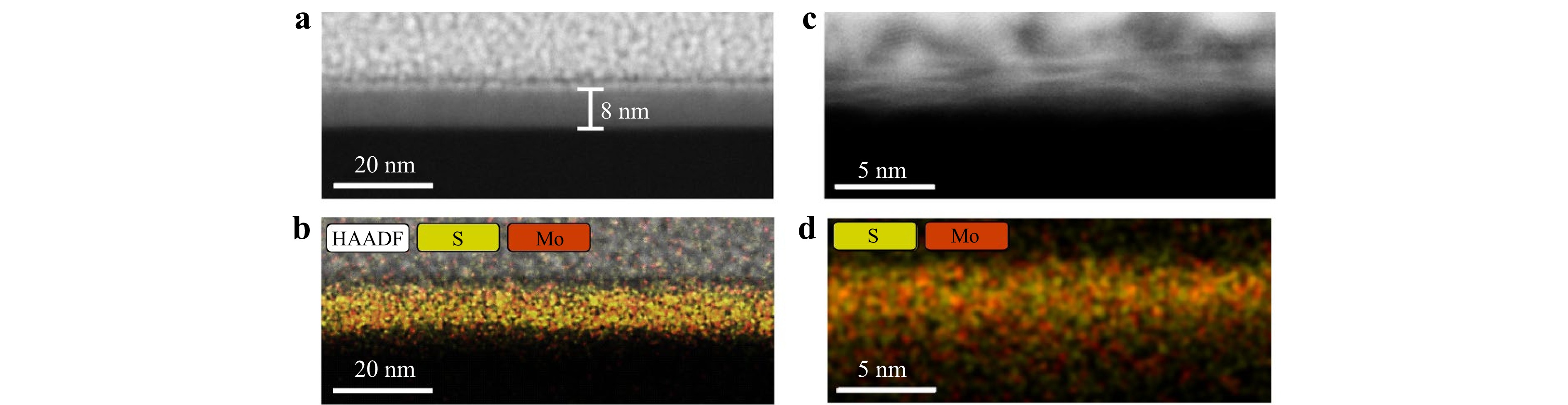
Fig. 2 STEM and EDS of the laser-processed tracks produced from (NH4)2MoS4 precursor. a STEM image of a track formed using an irradiation intensity of 0.5 MW/cm2, showing an amorphous material layer and b EDS map of the corresponding area, mapping the distribution of Mo and S. The S/Mo ratio measured from EDS was found to be 3. c STEM image of the synthesised MoS2 track, after global thermal annealing of the pre-patterned amorphous structure and d corresponding EDS map showing the Mo and S distribution. The indicated S/Mo ratio was ≈ 2.
The second processing step (thermal annealing) applied to this sub-threshold-irradiated material completed the synthesis process. The pre-patterned amorphous MoS3 can be converted into polycrystalline MoS2 by post-annealing, either through subsequent laser irradiation at a higher intensity or by global thermal annealing in an inert atmosphere (see Fig. S2 of the Supplementary Material). A STEM image of the track after global thermal annealing is shown in Fig. 2c. In this case, we obtained a layered material with a thickness of 2.5 nm and a polycrystalline structure. The corresponding EDS analysis (Fig. 2d) of the area after thermal annealing showed an S/Mo ratio of ~2. This, along with the observed layered structure shown in the STEM image, indicated the full conversion of the precursor to MoS2 as a result of the two-step synthesis process.
Pre-patterning with low-intensity laser irradiation, as described above, enables high-spatial-resolution patterning using interferometric methods, producing periodic microstructures. These periodic patterns can be used as diffractive optical elements with a very high refractive index contrast arising from the TMDC. A Michelson interferometric arrangement was used to adjust the angle between the interfering beams, thereby controlling the periods of the interference fringes (Fig. S3). This arrangement was used for both visible (532 nm) and UV (244 nm) laser sources. The periodic structures were fabricated on the SiO2/Si and LiNbO3 substrates. In these experiments, the pre-patterned gratings were post-processed in a tube furnace to produce MoS2 and WS2. Post-annealing was performed at 750 °C for MoS2 and WS2 in inert atmosphere. Examples of the gratings produced using this interference exposure are shown in Fig. 3. The shortest period achieved was 150 nm, consisting of periodic MoS2 stripes with a width of 90 nm and length of ~800 µm, corresponding to an aspect ratio close to 104. Fig. 3a shows an SEM image of this structure and Fig. 3b shows a WS2 grating with a period of 540 nm produced using the same method. Furthermore, by applying two successive exposures, combined with a 90° sample rotation between exposures, we produced a 2D periodic square grid with a period of 630 nm, as shown in Fig. 3c.
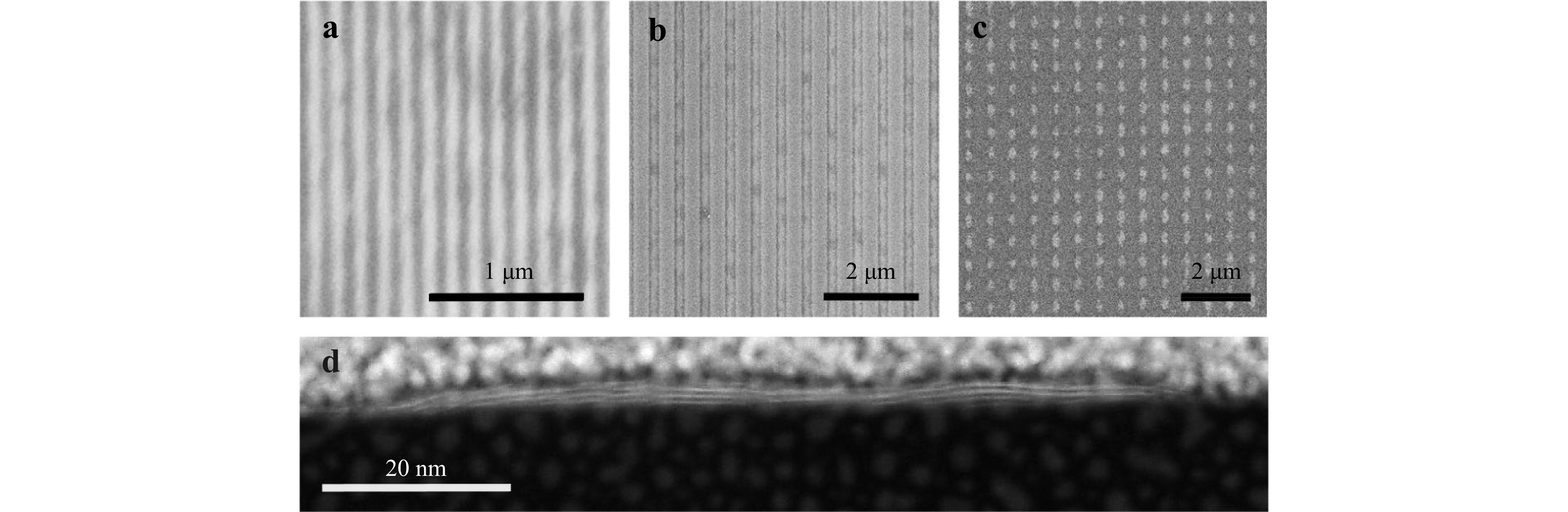
Fig. 3 SEM/STEM of the laser-synthesised gratings. SEM images of a MoS2 linear grating with a period of 150 nm, b WS2 linear grating with a period of 540 nm and c MoS2 2D square grating with a period of 630 nm. All gratings were fabricated on SiO2/Si substrate. d Cross-sectional STEM image of a single grating period showing the layered structure of the synthesised MoS2.
Transmission electron microscopy (TEM) of a single grating stripe (Fig. 3d) revealed three layers of MoS2 conforming to the substrate, whereas there was no MoS2 between successive stripes. We noted that the TMDCs produced in this manner were polycrystalline in nature. Grain boundaries can be a source of wavelength-dependent scattering losses in the propagating media. However, if the transit length of light through the medium is short, then these losses are negligible. The grain size as a function of the grating period is shown in Fig. S4 of the Supplementary Material. The average lateral grain size, estimated from multiple TEM images corresponding to several grating periods, was ~30 nm. Subsequent EDS mapping of the region between the grating stripes (Fig. S4) showed the absence of the material in the intermediate region, thereby confirming a high grating contrast.
The diffraction efficiencies of the gratings produced on SiO2/Si substrates, which consisted of a few layers of MoS2, were measured at 633 and 532 nm. The diffraction efficiencies quoted here corresponded to the ratio of the diffracted optical power in a single diffraction order, divided by the power of the incident beam. We found that the diffraction efficiencies were within a range of ~0.1–1%, depending on the probe wavelength, material thickness, and incident light polarisation (Fig. 4a). These values matched those reported in the literature2 for TMDC structures with a few layers, which typically range from ~0.01% (monolayer) to several per cent (multi-layer) at visible wavelengths under normal incidence.
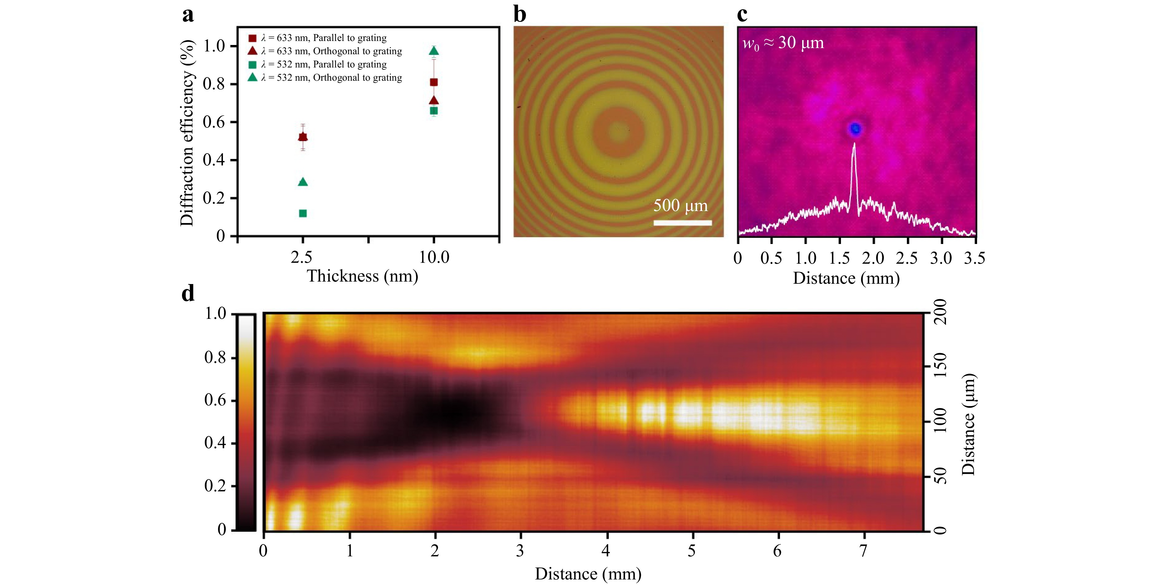
Fig. 4 TMDC gratings and Fresnel hologram functionality. a Diffraction efficiency of MoS2 gratings with two different thicknesses and a period of 630 nm, probed using 532-nm and 633-nm laser beams with variable polarisation. b Optical image of MoS2 Fresnel hologram fabricated on SiO2/Si substrate. c Focusing of a 633-nm laser beam by an MoS2 Fresnel hologram (focal length: 150 mm) produced on LiNbO3 substrate. The spot diameter at focal point was ≈ 60 μm. d Measured lateral cross-sectional intensity distributions along the optical axis (z-axis) of the Fresnel hologram on LiNbO3 substrate around its focal point.
We calculated the refractive index that was responsible for these diffraction efficiencies $ \eta $ using the formula $ \eta =J_{1}^{2}\left(2{\text{π}} \Delta nd/\lambda \cos \cos \theta \right) $ for lossless thin grating29, where $ d $ is the thickness of the grating structure, $ \lambda $ is the probing wavelength, $ \theta $ is the incident angle, and $ \Delta n $ is refractive index modulation. Applying this formula to the measured diffraction efficiency of 2.5-nm-thick MoS2 grating at normal incidence yielded a refractive index of 6.8 ± 0.4 at 633 nm and 4.6 ± 0.1 at 532 nm.
In addition, other 2D structures, such as Fresnel holograms, were produced using an interferometric approach. An optical image of the lens is shown in Fig. 4b. The intended focal lengths of the Fresnel hologram were 170 mm at 532 nm and 150 mm at 633 nm. Fig. 4c shows the focusing of a laser beam (λ = 633 nm) by an MoS2 Fresnel hologram, which was fabricated on a surface of bulk single-crystal lithium niobate (z-cut). Fig. 4d presents the cross-sectional intensity distributions along the y- and z-axes near the focal plane of the Fresnel hologram. We observed a well-defined focusing spot in the lateral dimensions. The spot diameter at the focal point was ~60 µm at 633 nm, and the measured Rayleigh length, estimated from the intensity contours of Fig. 4d, was 15.7 mm. The diffraction-limited spot diameter for such a structure was calculated to be 52.7 µm, which was ~12% smaller than the measured value. The focusing efficiency measured in our Fresnel hologram ranged from 0.1% at λ = 532 nm to 0.4% at λ = 633 nm. The focusing efficiencies measured in a similar structure consisting of exfoliated monolayer WS2 were within a range of 0.03–0.1% in the visible spectral region24. The higher focusing efficiency measured in our case is attributed to the greater thickness of the TMDC.
We further estimated the MoS2 refractive index using spectroscopic ellipsometry. For the modelling, we assumed an infinite Si slab with a 300-nm-thick oxide layer and 10-nm-thick MoS2 layer. Based on previous spectroscopic ellipsometry studies of the MoS2 refractive index25,30, we used the N Tauc-Lorentz (TL) oscillator model to fit the permittivity. According to the TL model, the permittivity $ {\varepsilon }_{2} $ can be expressed as:
$$ {\varepsilon }_{2}=\{\frac{1}{E}\cdot \frac{A{E}_{0}C{\left(E-{E}_{g}\right)}^{2}}{{\left({E}^{2}-E_{0}^{2}\right)}^{2}+{C}^{2}{E}^{2}}\;for\;E> {E}_{g}0\;for\;E< {E}_{g} $$ (1) where $ E $ is the photon energy, $ A $ is the oscillator strength, $ {E}_{0} $ is the resonance frequency, and $ C $ is the oscillator broadening. The $ {\varepsilon }_{1} $ is obtained from $ {\varepsilon }_{2} $ using Kramers-Kronig integration. The selected fitting parameters are listed in Table S1 of the Supplementary Material. The quality of the model was assessed based on the mean squared error (MSE). The MSE in our calculations was ≈ 3 for all measurements, which, according to previous reports25, was sufficient for this type of material. The estimated optical constants are presented in Fig. 5a, revealing refractive indices within a range of 3.2–4.4.
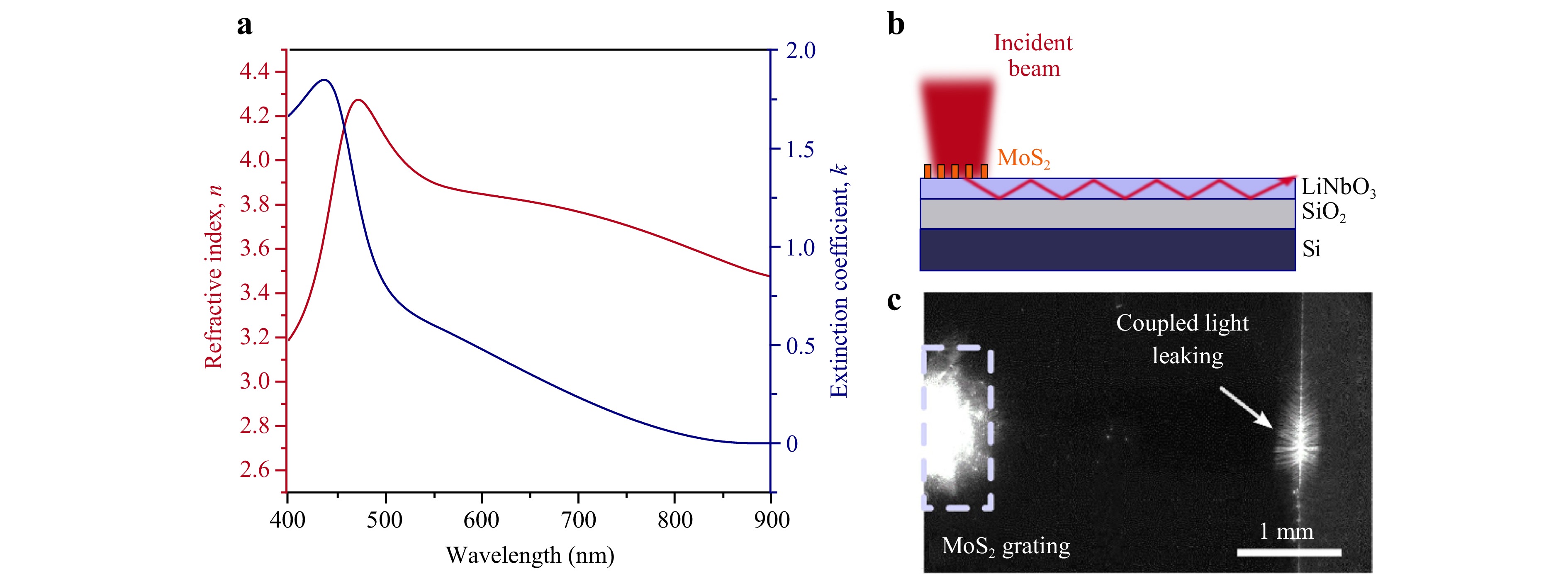
Fig. 5 Optical properties and light coupling behaviour of MoS2-based grating structures. a Optical constants (n and k) for the 10-nm-thick MoS2 film on SiO2/Si substrate obtained from ellipsometry spectra. b Schematic representation of laser beam coupling inside a 0.7-µm-thick lithium niobate film on 10-µm-thick layer of SiO2 planar waveguide, using an MoS2 grating coupler. The beam directed on the grating (left side) coupled the diffraction order in the lithium niobate on top of the SiO2/Si. The order propagated through the lithium niobate film and could be observed on the opposite side of the waveguide system (right side) as light leakage from the edge of the substrate. c Experimental observation using charge-coupled device (CCD) camera showing coupling of 633-nm laser inside a 0.7-µm-thick lithium niobate film on 10-µm-thick layer of SiO2 planar waveguide, using an MoS2 grating coupler. The bright point of the left side of the CCD camera image corresponded to the position of illuminated grating coupler, whereas the second bright region near substrate edge (on the right side) arose from coupled light leakage after propagation through the substrate.
We fabricated an MoS2 grating with a period of 3 µm onto thin-film lithium niobate, consisting of a 0.7-µm-thick z-cut lithium niobate film bonded to a 10-µm-thick SiO2 layer, forming a planar waveguide. MoS2 grating was used to couple visible light (633-nm He-Ne laser beam) into a propagating mode of this planar waveguide. Fig. 5b shows a schematic representation of laser beam coupling inside the thin-film lithium niobate layer. The corresponding camera image of the He-Ne beam coupling into the thin-film lithium niobate is shown in Fig. 5c. The bright point of the left side corresponds to the position of the illuminated grating coupler, whereas the additional bright region near the substrate edge (right side) is associated with the light leaking from the opposite edge of the waveguide, after propagating through the film.
-
Optical microscopy and Raman spectroscopy analyses of the developed laser-irradiated precursor film revealed three distinct regimes of structural transformation as a function of the irradiation laser intensity: (i) pre-patterning of the precursor with the formation of an amorphous structure, (ii) synthesis of a polycrystalline material, and (iii) laser-induced thinning. Although TMDC microstructures can be obtained by direct laser synthesis, these structures can be significantly limited by the beam spot size and temperature distribution, which are associated with the Gaussian beam profile. This causes undesired variations in thickness and crystallinity across the track. However, according to STEM and optical analyses, the sub-threshold amorphous structure was less sensitive to the Gaussian beam intensity distribution and exhibited a more uniform profile.
It has been reported in the literature22,23 that the products of the thermal decomposition of thiosalt precursors depend on the processing temperature. In inert atmosphere, the thermal decomposition of ammonium tetrathiomolybdate ((NH4)2MoS4) to form crystalline MoS2 occurs within a temperature range of 300–800 °C. However, within a temperature range of 120–280 °C, (NH4)2MoS4 decomposes into amorphous MoS3 and MoS2.
Laser irradiation results in a localised energy transfer to the thiosalt film in the form of heat, which induces a thermochemical reaction that causes the film to decompose. Although it is challenging to directly measure the exact temperature attained by the laser-irradiated region, the range of temperatures to which the film is subjected can be deduced from the products of the laser-induced reaction22,23. In view of these observations, we can conclude that laser intensities within a range of 0.2–0.5 MW/cm2 correspond to the range of peak temperatures of 120–280 °C, where the peak temperature is the temperature at the peak of the Gaussian intensity distribution, which is expected to produce amorphous compounds.
Reducing the thermal load during processing enables high-resolution patterning of the precursor, including the formation of periodic structures, using interferometric techniques. Our results indicated that the mark-to-space ratio of the grating could be adjusted by controlling the laser intensity level. As shown in Fig. S5 of the Supplementary Material, there was a monotonic variance in the mark-to-space ratio from the centre to the periphery of the Gaussian intensity profile of the beams used to imprint the structure. In addition, the thicknesses of the resultant films could be adjusted by varying the initial precursor film thickness, which could be controlled by changing the precursor concentration in the spin-coating solution. Subsequent thermal annealing facilitated the transformation of these patterned regions into polycrystalline TMDC. Consequently, we were present with an opportunity to decouple the patterning and synthesis processes as well as optimise each step independently.
The conformity of the TMDC layers to the substrate, as shown in the TEM images of the synthesised material, suggests that the optical anisotropy, which is a consequence of structural anisotropy, is preserved14,15. The refractive index, as calculated from the diffraction efficiency of a 2.5-nm-thick grating (6.8 ± 0.4 at 633 nm and 4.6 ± 0.1 at 532 nm) was found to be ~30% higher than the values found in the literature25,26 for the same MoS2 thickness (3–4 layers). This overestimation stems from neglecting the absorption losses of the film in the calculations. However, we independently investigated the refractive index of the TMDC film using spectroscopic ellipsometry, which is a common method for estimating the optical constants of such materials8,9,25,30. Ellipsometry measurements indicated refractive indices in the range of 3.2–4.4 for a 10-nm-thick film, which were consistent with those reported for bulk MoS2 in previous studies26.
This finding, along with the observation that the layered material structure preserves the intrinsic optical anisotropy characteristics of the TMDC, suggests that the collective photonic response is comparable to that of pristine single-crystal flakes. Consequently, the fabricated structures hold significant potential for photonic applications such as the grating couplers demonstrated herein or other photonic nanostructures1,4. Moreover, the method outlined in this paper enables the fabrication of TMDC photonic structures directly on functional substrates such as lithium niobate, SiO2/Si, and other photonic substrates. The use of ferroelectric LiNbO3, in particular, has the potential of producing tuneable photonic structures via electro-optic and pyroelectric effects. In addition, this method can be used to fabricate TMDC nanostructures on flexible substrates. The caveat here is that one must ensure that the annealing temperature in the second step of the process is compatible with the temperature tolerance of the flexible substrate (which is often a polymer). To mitigate the temperature constraints imposed by the substrate, it is possible to substitute the furnace annealing step with consecutive laser exposure at a higher intensity to complete the synthesis step. Finally, the pre-patterned/laser-synthesised area in the direct-writing mode is defined by the range of the translation stages, which can be in the order of metres by modern standards, and thus able to process rather large substrate surfaces. In the holographic mode, the processed area is defined by the power of the irradiation laser beam. Here, we showed the results obtained using unfocused laser beam spots (≈ 3 mm in diameter). This suggests that the proposed laser-based lithographic approach for the production of TMDC photonic nanostructures is potentially scalable and adaptable for hybrid electro-optic architectures that allow the bridging of passive diffractive elements with active control mechanisms, which are essential for photonic systems.
In conclusion, we have demonstrated a laser lithography process in this study, which was applied directly onto Mo and W thiosalt precursors to produce a range of diffractive optical elements consisting of MoS2 and WS2 with resolutions down to 90 nm. The diffractive optical elements were comparable to those achieved using more complex and expensive methods, such as FIB and electron beam lithography. The nanostructure and composition analysis of the microstructured films revealed their polycrystalline nature and few-layer thicknesses. The layers conformed to the substrate, preserving the optical anisotropy implied by the layered structure. We have also fabricated 1D and 2D gratings, including a Fresnel hologram and a grating coupler, using interferometric and direct-writing approaches and we found that their estimated refractive indices matched those found in the literature. Finally, we characterised these structures in terms of their diffraction efficiency and focusing. Our results demonstrated the potential of our approach for producing photonic structures from this emerging class of functional materials.
-
MoS2 and WS2 precursors were prepared from ammonium thiosalts ((NH4)2MoS4 and (NH4)2WS4). For the MoS2 precursor, we dissolved 31 and 61 mg of (NH4)2MoS4 (corresponding to concentrations of 24 and 48 mM, respectively) in 1 mL of ethanolamine, 2 mL of butylamine, and 2 mL of dimethylformamide (DMF). To obtain a 100-mM (NH4)2WS4 solution, 200 mg of thiosalt was dissolved in 1 mL of ethanolamine, 2 mL of butylamine, and 2 mL of N-methyl-2-pyrrolidone (NMP). The precursor solutions were applied to the intended substrates via spin coating. The rates were set at 3,500 and 6,500 rpm for (NH4)2MoS4 and (NH4)2WS4, respectively. The ramp speed and spin-coating time were set at 500 rpm and 1 min, respectively, for both precursors. The coated substrates were heated on a hot plate (90 °C for molybdenum precursor and 180 °C for tungsten precursor) to enable evaporation of the solvents and solidification of the film.
The Si/SiO2 substrates (1.5 cm × 1.5 cm) were obtained from a 4-inch doped n-type silicon wafer with a 300-nm-thick oxide layer. LiNbO3 substrates (z-cut) were obtained from a 300-μm-thick 3″ wafer. Thin-film LiNbO3 (0.7 µm of z-cut lithium niobate on a 10-µm-thick SiO2 layer) was used to produce the grating couplers. Each substrate underwent a cleaning procedure involving sequential immersion in acetone, isopropanol, and deionised water, with each step followed by a 5-min treatment in an ultrasonic bath to remove contaminants and prevent defect formation during spin coating of the film. The substrates were dried using N2 gas flow after each processing step. To ensure good adhesion between the precursor solution and substrate, the cleaned substrates were surface-treated in Ar/N2 plasma for 15 min.
-
A visible laser system at a wavelength of 532 nm (Coherent-Verdi G20 CW) and a UV laser source at a wavelength of 244 nm (Coherent Innova 300C MotoFRED) were used for laser processing of the precursor films.
A power test was performed using single-beam laser writing with a 532-nm laser beam. The samples (obtained using 24-mM Mo thiosalt precursor) were placed onto a high precision x-y translation stage system (Aerotech ANT95XY). A high-magnification objective allowed the application of a spot size at a focal point of 1.36 μm. The speed was set at 20 m/s. The intensity range for the exposures was 0.2–1 MW/cm2.
The grating structures were produced using laser interference patterning. For visible laser irradiation (532 nm), the peak intensity of each interfering beam was set at 0.3 kW/сm2. The pattern was formed by static 2-s exposure of the precursor. For the UV pre-patterning, the single interfering beam intensity and exposure time were set at 0.75 W/cm2 and 30s, respectively. The period of the interference pattern was defined as the angle between the interfering beams.
The Fresnel hologram was fabricated from a 48-mM MoS2 precursor solution using the interference of two beams (wavelength: 532 nm, spot diameter: 3 mm). After passing through a plano-convex singlet lens (focal length: 150 mm), the collimated reference beam interfered with a second beam with a curved phase front. The focal length of the resultant structure was determined by the geometry of the hologram recording arrangement; specifically, the recording beam wavelength, inserted lens focal length, and sample position relative to the beam intersection.
-
The subsequent thermolysis step applied to the amorphous pre-patterned material was performed separately using either high-intensity laser or high-temperature furnace annealing. High-intensity laser annealing was performed using a focused laser beam at 532 nm under ambient conditions. The beam intensities required to complete the syntheses of MoS2 and WS2 were within a range of 2–2.6 MW/cm2.
Thermal annealing was performed by high-temperature treatment in a furnace under an inert atmosphere. The furnace temperature was set at 750 °C. To remove air from the system after heating, the furnace was sequentially purged with Ar gas at a flow rate of 100 sccm and an Ar/H2 gas mixture at a flow rate of 75/25 sccm for 40 min each. The sample was then annealed for 30 min using 99 sccm of Ar and 1 sccm of N2. After annealing, the sample was left for 40 min in a cold zone under a 1 sccm of H2 flow until it reached room temperature. All structured samples were covered with a substrate coated with a uniform precursor film to prevent etching of the structure.
-
Raman spectroscopy was performed using a LabRAM HR Evolution confocal Raman microscope (HORIBA, France) with an excitation wavelength of 532 nm at room temperature. The spectra were obtained from the central area of the interference-patterned area and from the central area of individual tracks in the direct-writing case.
Scanning electron microscopy (SEM) was performed using a Quattro ESEM scanning electron microscope (Thermo Fisher Scientific, Czech Republic). Lamellae for subsequent STEM analysis were prepared by focused ion beam (FIB) milling using a Helios G4 PFIB UXe DualBeam system (Thermo Fisher Scientific, the Netherlands). A Titan Themis Z transmission electron microscope (Thermo Fisher Scientific, Breda, the Netherlands) was used to obtain the STEM images and EDS maps of the amorphous and synthesised structures of MoS2. The concentration of Mo thiosalt in all STEM investigations was 24 mM.
-
Ellipsometry measurements were conducted on a uniform area of MoS2 with a size of 4 mm × 4 mm that was produced by two-step processing of the thiosalt precursor film. The (NH4)2MoS4 precursor solution was prepared at a concentration of 48 mM and spin-coated onto a SiO2/Si substrate. To cover a large surface area, a low-intensity irradiation step was performed by partially overlapping tracks produced by raster scanning of a continuous wave laser beam at 532 nm (Coherent-Verdi G20) to form a uniform pre-patterned patch consisting of amorphous material. A raster scanning pitch of 0.5 μm was applied to ensure uniformity of the pre-patterned film. An Olympus Plan Fluorite Objective RMS40X-PF objective lens, providing a 1.4-μm spot diameter at focus, was used. The scanning speed used for the pre-patterning exposure was 20 mm/s and the laser power was 15 mW. After dissolution of the unexposed area in organic solvents (see Materials and Methods, Laser processing), the sample was annealed in a furnace under an inert atmosphere (see Materials and Methods, thermolysis step) to complete the synthesis of the MoS2 films.
To estimate the optical constants, a SENresearch 4.0 variable-angle spectroscopic ellipsometer (SENTECH Instruments GmbH, Germany), operating within a wavelength range of 400–900 nm, was used. The ellipsometric data were collected at incident angles of 50, 60, and 70°. Fitting of the measured spectra was performed using SpectraRay/4 spectroscopic ellipsometry software, where the Fresnel multi-layer model was used for a 10-nm-thick MoS2 layer on a 300-nm-thick SiO2 layer. The thickness of the bottom Si layers was assumed to be infinite. Permittivity fitting was performed using a three Tauc-Lorentz (TL) oscillator model.
-
The diffraction efficiency of the gratings and the focusing performance of the Fresnel hologram were characterised using a 633-nm JDSU He–Ne laser and 532-nm Coherent Verdi G20 CW laser sources.
MoS2 gratings with thicknesses of 2.5 and 10 nm were prepared from 24-mM and 48-mM precursor solutions. The diffraction efficiencies of the gratings were calculated as the ratio of the power contained in the first diffraction order to the incident power for two distinct laser wavelengths (532 and 633 nm). The laser beam was directed at normal incidence to the sample surface. To eliminate the contribution of scattered light, we placed the photodetector at a distance of 0.4 m away from the sample and employed two iris diaphragms, one placed near the sample and the other directly in front of the detector. This set-up isolated the directional diffraction order while excluding non-directional scattered light. Consequently, any residual scattered light in our signal was limited to the portion confined to the solid angle defined by the two iris diaphragms and was reduced with distance according to the 1/R2 law. The measurements were conducted for both s- and p-polarised beams.
To investigate the focus of the Fresnel hologram, the sample was mounted on a translation stage that allowed linear shifting of the lens along the z-axis. The Fresnel hologram was illuminated by collimated laser beams at wavelengths of 633 and 532 nm. Focal spot profiles at various positions were recorded using a Newport LBP2-HR-VIS2 laser beam profiler (Newport Corporation, United States of America). The lateral cross-sectional intensity distributions along the optical axis (z-axis) were measured using a custom imaging system. Focal spot profiles were captured using a charge-coupled device (CCD) camera (DCC1545M) equipped with a 4× objective lens (NA = 0.10) and tube lens (f = 300 mm), yielding a system magnification of 16.2×. Thus, each CCD pixel corresponded to a lateral step size of 320 nm. Three-dimensional focal spot reconstruction was obtained by stacking images acquired at incremental lens-to-objective distances, adjusted via a 1D scanning stage with ≈ 50-μm steps.
-
The authors wish to acknowledge the Advanced Imaging Core Facility (AICF) at the Skolkovo Institute of Science and Technology for their technical support with the SEM and TEM measurements. The authors graciously acknowledge Prof Albert. G. Nasibulin and Dr Dmitry V. Krasnikov for their assistance with the thermal annealing experiments, and the Plasmonics Laboratory, Center for Engineering Physics, Skolkovo Institute of Science and Technology, for access to the Raman spectroscopy equipment.
Laser printing of 2D transition metal dichalcogenide diffractive optical elements
- Light: Advanced Manufacturing , Article number: 63 (2026)
- Received: 30 December 2025
- Revised: 09 April 2026
- Accepted: 10 April 2026 Published online: 26 May 2026
doi: https://doi.org/10.37188/lam.2026.063
Abstract: Transition metal dichalcogenides (TMDCs) are promising layered materials for nanophotonics because of their inherent optical anisotropy, large refractive indices, and optical non-linearity, which make them excellent candidates for integration into photonic components. However, current prototyping techniques used to fabricate functional photonic elements rely on post-processing of single-crystal flakes or chemical vapour deposition (CVD)-grown films via focused ion beam milling, which is a throughput-limited and time-consuming approach. Therefore, scalable and rapid patterning methods for TMDC-based photonic devices are required to boost their application in the field of photonic technologies. Herein, we present a laser lithography method that enables the direct production of ultrafine diffractive MoS2 and WS2 structures from their chemical precursors. Thin films of thiosalt precursors, spin-coated onto various substrates, can be patterned with high resolution when exposed to light in the visible and ultraviolet (UV) spectral regions in a photolithographic manner. This allows either the direct synthesis of TMDC structures or the production of micro/nanopatterns consisting of partially synthesised amorphous material from the initial precursor films, which can later be converted to the desired TMDC using a two-step process. Using interferometric lithography, we fabricated of MoS2 and WS2 diffraction gratings with periods as short as 150 nm and aspect ratios ~104 (length/width), as well as MoS2 Fresnel holograms on photonic substrates such as silica (SiO2) and lithium niobate (LiNbO3). An MoS2 grating coupler was fabricated and used to couple light onto a thin-film lithium niobate planar waveguide. The measured diffraction efficiencies of the laser-patterned multi-layer MoS2 gratings at visible wavelengths matched the corresponding values reported for exfoliated TMDC materials, highlighting the potential of this method for fabrication of 2D photonics.
Research Summary
Thin-film optics: Laser-printing of 2D-TMD diffractive optical structures
Ultra-thin 2D semiconductors, offer exceptional optical responses that enable the fabrication of small-scale, high-performance photonic structures such as diffractive structures. Few-layer, atomically thin transition metal dichalcogenides (TMDCs), possess high refractive indices, optical nonlinearity and optical anisotropy and interact strongly with light. Therefore are suitable for the fabrication of miniaturized photonic elements. Arina Kalganova from Skolkovo Institute of Science and Technology (Skoltech) and colleagues now report on a laser-assisted method for the production of TMDC diffractive optical elements directly from chemical precursors. Localized laser irradiation induces chemical reactions in these precursors, which eventually lead to spatially selective synthesis of functional TMDCs. This scalable technique rapidly delivers high-resolution gratings and lenses on various photonic substrates. The team demonstrated applications including grating couplers for chip integration and thin-film focusing elements.
Rights and permissions
Open Access This article is licensed under a Creative Commons Attribution 4.0 International License, which permits use, sharing, adaptation, distribution and reproduction in any medium or format, as long as you give appropriate credit to the original author(s) and the source, provide a link to the Creative Commons license, and indicate if changes were made. The images or other third party material in this article are included in the article′s Creative Commons license, unless indicated otherwise in a credit line to the material. If material is not included in the article′s Creative Commons license and your intended use is not permitted by statutory regulation or exceeds the permitted use, you will need to obtain permission directly from the copyright holder. To view a copy of this license, visit http://creativecommons.org/licenses/by/4.0/.

 DownLoad: