



-
Terahertz (THz) waves typically refer to electromagnetic (EM) waves covering a frequency spectrum from 0.1 to 10 THz, which is located at the interface regime between electronics and photonics1,2. The novel EM properties, such as low photon energy, distinct fingerprint spectrum, and high penetrability, make THz technology highly applicable in next-generation wireless communications, security detection, medical diagnosis, and imaging3–6. Therefore, the manipulation of THz waves in the desired manner has emerged as an important topic in scientific researches and practical applications. Among numerous functional devices, the high-performance and ultra-compact platform capable of manipulating polarization states of THz waves are highly desired in various applications7–9. Unfortunately, conventional THz wave plates are usually of bulky sizes, low efficiencies and operate in a limited frequency band due to the weak interactions between natural materials and THz waves10,11.
In recent years, the rapid developments of metasurfaces have provided new opportunities for the realization of ultra-compact, small-footprint, and multifunctional devices working at different frequency regimes12–16. Specifically, metasurfaces are two-dimensional (2D) metamaterials constructed by planar microstructures (i.e., meta-atoms) with meticulously designed EM responses that are arranged in specific global sequences17–20. They have attracted considerable attention due to their strong capabilities to manipulate EM waves in subwavelength level. Many fascinating wave-manipulation effects have been realized, such as anomalous reflection/refraction17,18,21,22, surface wave excitation and manipulations23–30, light beam focusing31–35, specific- or multi- functional holographic imaging36–42, complex beam generation43–47, and so on. While metallic metasurfaces are widely utilized to tailor the wavefront of light waves through various resonance modes, they still face significant challenge of considerable intrinsic ohmic loss, which hinder their potential applications48. Recently, dielectric metasurfaces exhibit significantly lower absorption losses compared to the metallic counterparts, paving a new way for optical field manipulations49–52.
While reviewing the advancements of all-dielectric meta-devices, we find that they usually encounter performance limitation in practical implementation20,53,54. Relying on the phase accumulation effect for light controls, the dielectric meta-atoms usually require the high aspect-ratio (AR), implying that their practical fabrication necessitates the complicated deep etching technique34,55–57. During this process, various fabrication imperfections, such as vertical etching depth error and lateral morphology error, commonly occur and negatively affect the performance of the device58. Therefore, it is crucial to develop an optimized deep-reactive-ion-etch (DRIE) technology for creating high-efficiency dielectric meta-devices in THz and other frequency regimes, which may significantly enhance their practical applications. In addition, dielectric meta-devices are often made by high-index dielectric materials, which may also experience significant reflection loss due to impedance mismatch issue55,59,60.
In this work, we theoretically design and experimentally demonstrate transmissive dielectric metasurfaces for achieving high-efficiency and broadband THz wave manipulations, as schematically shown in Fig. 1a. Based on the Bosch etching technology [see Fig. 1c], we successfully construct the high-resistance lossless silicon pillar meta-atoms with high AR (about 19.2:1), yielding high transmission efficiency and full range of phase modulations. As a proof-of-concept, we create two THz meta-polarizers, including a half-wave plate (HWP) for achieving linear-linear polarization conversion and a quarter-wave plate (QWP) for achieving linear-circular polarization conversion. We numerically demonstrate that the vertical etching depth and lateral morphology significantly affect the performance of the meta-devices. Therefore, we propose an optimized fabrication methodology to develop high-quality silicon meta-devices. Experimental measurements indicate that the fabricated meta-HWP and meta-QWP possess high polarization conversion ratios (PCRs) of 0.6 within 0.6–0.8 THz (relative bandwidth: 28.57%) and 0.5–0.8 THz (relative bandwidth: 46.15%). The highest PCRs measured can reach 0.915 and 0.99 at approximately 0.73 THz and 0.66 THz, respectively. All experimental results are highly consistent with the full-wave simulations, confirming the effectiveness of the proposed fabrication methodology. Finally, we construct a Pancharatnam-Berry (PB) typed metalens with a high numerical aperture (NA) of 0.8 at 0.7 THz based on the proposed high-performance HWP meta-atoms, and experimentally verify that the average focusing efficiency can be well maintained at about 85.56% in the range of 0.6–0.8 THz.
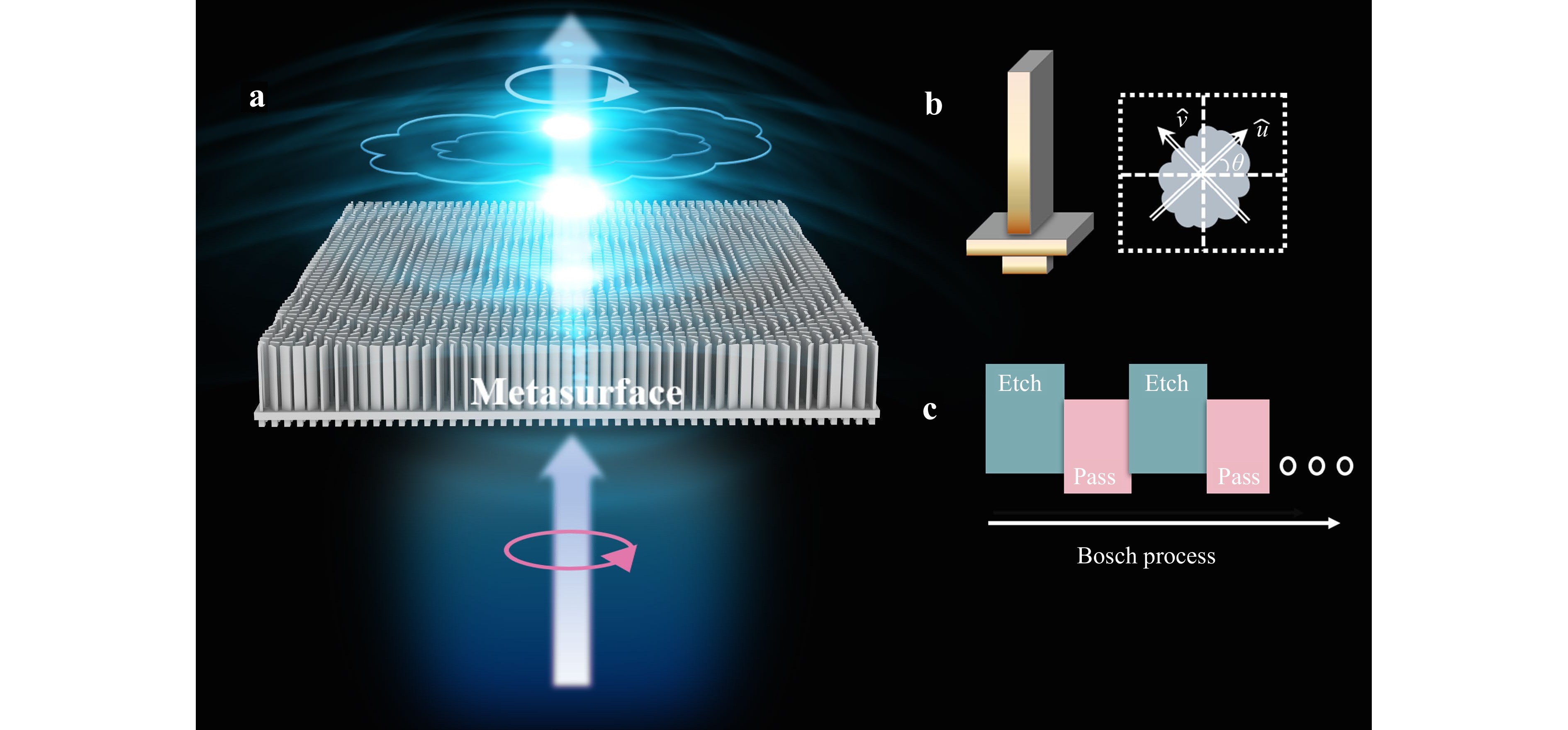
Fig. 1 Realization of dielectric meta-devices for achieving high efficiency wave manipulations. a Schematic of the high-efficiency wave-controls by the proposed dielectric meta-devices. b Schematic of the adopted high aspect-ratio (AR) dielectric meta-atom satisfying the mirror system along two principal axes u and v. c Schematic of the deep-reactive-ion-etch technique to fabricate the high AR meta-atom depicted in b.
-
We first introduce the theoretical design of the desired THz meta-devices as shown in Fig. 1. All proposed devices are constructed by the silicon meta-atom satisfying the mirror system as shown in Fig. 1b, whose transmission and reflection properties can be described by diagonal Jones matrices $ \boldsymbol{T}(\mathbf{0})=\left(\begin{matrix}{t}_{uu} & 0\\0 & {t}_{vv}\end{matrix}\right) $ and $ {\boldsymbol R}(\mathbf{0})=\left(\begin{matrix}{r}_{uu} & 0\\0 & {r}_{vv}\end{matrix}\right) $. Here, $ {t}_{uu} $, $ {t}_{vv} $ and $ {r}_{uu} $, $ {r}_{vv} $ denote the co-polarized transmission and reflection coefficients of the proposed meta-atoms under the excitation of the EM waves linearly polarized along the two principal axes (i.e., u and v), respectively. To achieve high-efficiency light manipulation, the desired meta-atoms designed in the transmission configuration should be highly transparent (i.e., $ \left| {t}_{uu}\right| =\left| {t}_{vv}\right| =1 $, $ \left| {r}_{uu}\right| =\left| {r}_{vv}\right| =0 $). While the meta-atoms are rotated by an angle of $ \theta $ (defined as the angle between the u axis of the meta-atom’s local coordinate system and the x axis of the laboratory coordinate system) as shown in Fig. 1b, the Jones matrix of the meta-device can be expressed as $ {\boldsymbol T}(\theta )={\boldsymbol{S}}^{-1}\left(\theta \right)\boldsymbol{T}(\mathbf{0})\boldsymbol{S}\left(\theta \right) $, where $ \boldsymbol{S}\left(\theta \right)=\left(\begin{array}{cc}\cos \theta & \sin \theta \\-\sin \theta & \cos \theta \end{array}\right) $ is the transformation matrix connecting the local coordinate system and the laboratory coordinate system.
Utilizing the Jones matrix analysis, we can derive the theoretical criterion to design the high-performance meta-HWP satisfying the mirror symmetry (see more details in S1 of the Supplemental Material):
$$ \begin{array}{l} \begin{cases} \left| {t}_{uu}\right| =\left| {t}_{vv}\right| =1\\ \Delta \phi =\arg \left({t}_{uu}\right)-\arg \left({t}_{vv}\right)={\text{π}} \\ \theta =\dfrac{{\text{π}} }{4} \end{cases} \end{array} $$ (1) Equation (1) indicates that the desired meta-HWP should be totally transparent along two principal axes and possess the phase difference of $ {\text{π}} $ for two cross linear polarization (LP) cases. All meta-atoms of the meta-device should have the identical orientation angle of $ \theta ={\text{π}} /4 $. For the design of meta-QWP, the following conditions can be simply derived as (see more details in S1 of the Supplemental Material):
$$ \begin{array}{l} \begin{cases} \left| {t}_{uu}\right| =\left| {t}_{vv}\right| =1\\ \Delta \phi =\arg \left({t}_{uu}\right)-\arg \left({t}_{vv}\right)=\dfrac{{\text{π}} }{2}\\ \theta =\dfrac{{\text{π}} }{4} \end{cases} \end{array} $$ (2) Equation (2) implies that the desired meta-QWP should be totally transparent along two principal axes and possess the phase difference of π/2 for two cross LP cases. The orientation angle of all the meta-atoms on the meta-device should be π/4. In addition, while the phase difference ∆ϕ is equal to −π/2, the meta-device can realize another kind of LP-CP conversion.
-
We now adopt the proposed strategy to construct the meta-atoms for creating the high-performance transmission-type meta-devices working in the THz regime. As shown in Fig. 2a, the proposed building block consists of an amorphous silicon rectangular pillar with a high AR as the top layer, a continuous silicon spacer in the middle, and a square silicon microstructure as the bottom layer. Here, the high rectangular silicon pillar can offer a large phase difference ($ \Delta \phi $) by means of the accumulated anisotropic transmission phases for the input THz waves of different LPs. Meanwhile, while amorphous silicon is almost lossless in the THz regime, such pillar structures possess the limited effective mode index, thus giving rise to the high transparency property. To address the large impedance mismatch issue between the silicon spacer and the air, the square-shape silicon microstructure is introduced as the anti-reflection layer. Since the effective index (or impedance) of the anti-reflection layer locates between the values of the air and bulky silicon, the reflection loss can thus be significantly suppressed. In our design, both the width and thickness of the anti-reflection layer have been carefully optimized to ensure the high transparency performance across the working band of the meta-device. In short, by fully optimizing the structural parameters, we can obtain the transmissive meta-atoms with high transmission efficiency and the arbitrary tailored $ \Delta \phi $.
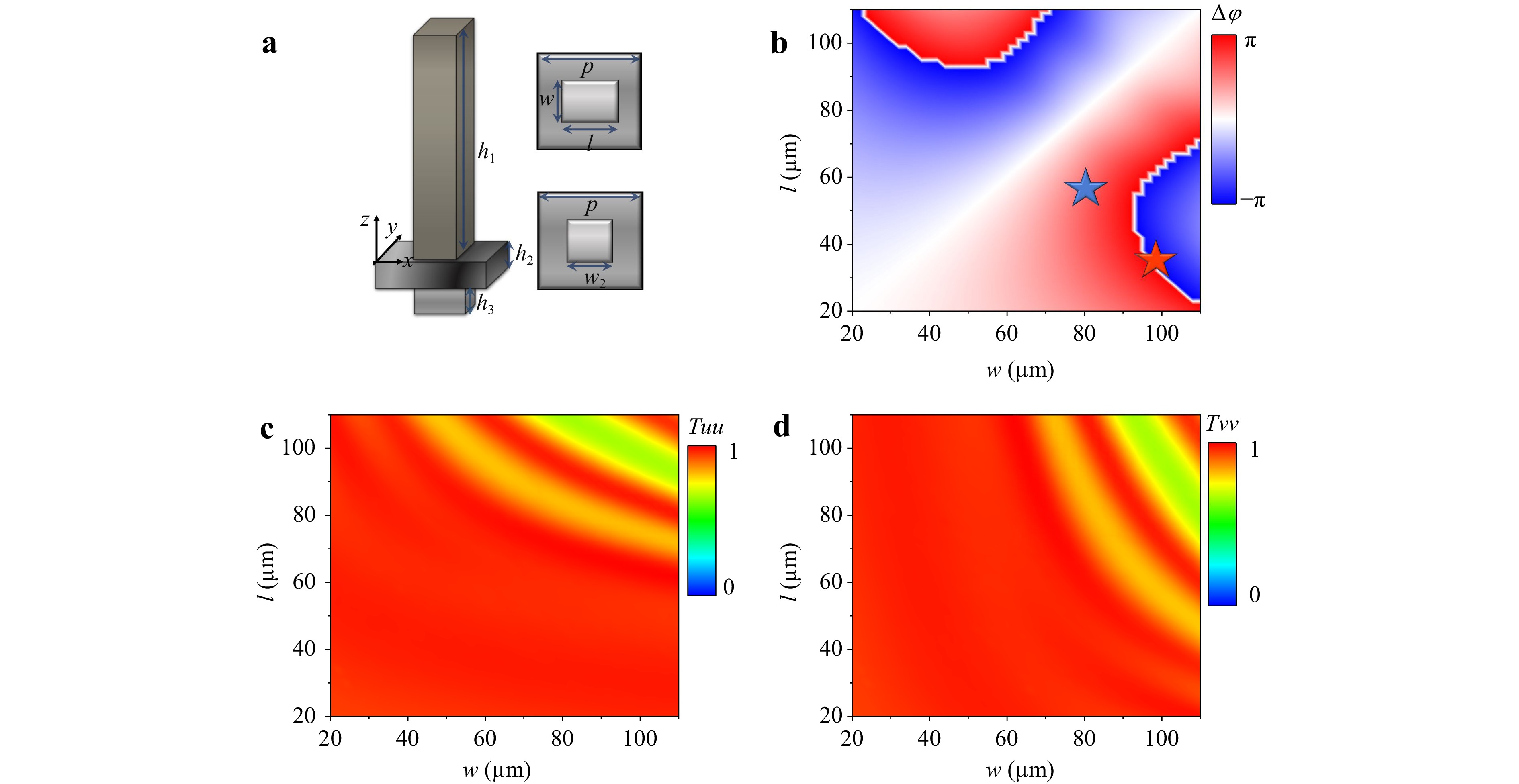
Fig. 2 Design of the proposed silicon meta-atom. a Schematic of silicon meta-atom consisting of high AR pillar (top), thin silicon spacer (middle) and an anti-reflection layer (bottom). b−d Simulated transmission phase difference ($ \Delta \phi =\arg \left({t}_{uu}\right)-\arg \left({t}_{vv}\right) $) and transmission efficiency ($ {T}_{uu} $ and $ {T}_{vv} $) of the silicon meta-atom arranged in periodic arrays with different $ l $ and $ w $ at the frequency of 0.7 THz.
To clarify the working mechanism of the meta-atoms, we start to explore the optical responses of the simplified structures, i.e., the free-standing rectangular silicon ($ {n}_{\text{si}}=3.35 $) pillars. For the normal incident beams carrying different LPs ($ \boldsymbol{E}||\hat{u} $ and $ \boldsymbol{E}||\hat{v} $), we investigate how the transmission characteristics of such periodic meta-atoms vary against the lateral sizes ($ l $ and $ w $). Here, the period ($ p $) and the height ($ {h}_{1} $) of the high AR silicon pillars are fixed as 125 and 480 $ \text{μm} $, respectively. Full-wave simulation results demonstrate that the high AR meta-atoms can provide sufficient phase difference $ \Delta \phi $ while maintaining high transmittances (See more details in S2 of the Supplemental Material). This clearly confirms that the proposed framework offers a broad design space capable of meeting the requirements of diverse polarization controls. Additionally, compared to the low AR counterparts, the high AR dielectric meta-atoms demonstrate larger phase retardation accumulated along the propagation direction, enabling more deeply subwavelength lateral dimension. This characteristic offers substantial advantages for creating the various functional meta-devices.
After understanding the role played by the high AR silicon pillars, we next introduce the complete design of the dielectric meta-atoms utilized in practical applications. In the fabrication process, the high AR silicon pillar needs to lay on a flat silicon spacer as the supporting layer. However, since the refraction index of silicon is quite high, an additional silicon microstructure is designed at the bottom of the silicon spacer. This microstructure helps reduce the reflection loss of the whole meta-atom and is therefore called as the anti-reflection layer. Through numerical optimization, we have determined the following parameters for the desired anti-reflection layer: $ {h}_{3}=62\;\text{μm} $ and $ {w}_{2}=56\;\text{μm} $ (See more details in S3 of the Supplemental Material). It should be noted that, since the microstructure of the anti-reflection layer is isotropic, it does not contribute to the transmission phase difference $ \Delta \phi $ accumulated inside the whole device.
After obtaining all basic parameters of the three layers, we calculate the co-polarization transmittance ($ {T}_{uu} $ and $ {T}_{vv} $) and transmission phase difference ($ \Delta \phi $) of such high AR silicon meta-atoms as functions of two key modulation parameters (i.e., $ l $ and $ w $), as shown in Fig. 2b−d. All these results are obtained through finite-difference-time-domain (FDTD) simulations using Eastwave software. In our simulation setup, periodic boundary conditions are implemented around a single unit structure to effectively model an infinite periodic metasurface. One port is positioned 200 $ \text{μm} $ below the anti-reflection layer to emit the source wave, and another port is placed 200 $ \text{μm} $ above the silicon pillar to collect the transmission signal. Both the amplitude and phase of the transmission and reflection mode can be obtained through these two ports. Based on the phase diagram of design parameters, we can easily determine the optimal parameters for the high-performance HWP ($ l=100~\text{μm} $, $ w=30~\text{μm} $) and QWP ($ l=81~\text{μm} $, $ w=56~\mu \mathrm{m}) $ denoted as red and blue stars in Fig. 2b, respectively. We can see that the meta-atoms can serve as the ideal high-efficiency elements to tailor the polarization of input THz waves. Finally, to quantitatively evaluate the performance of the created HWP and QWP, we can define their PCRs as:
$$ \begin{array}{l} {{PCR}}_{\text{HWP}}=\dfrac{1}{4}{\left| {t}_{uu}-{t}_{vv}\right| }^{2}\\ {{PCR}}_{\text{QWP}}={\left| \dfrac{{e}^{-i\cdot \frac{{\text{π}}}{4}\cdot \left({t}_{uu}\cdot \mathrm{cos} \left(\frac{{\text{π}}}{4}\right)+i{\cdot t}_{vv}\cdot \mathrm{sin} \left(\frac{{\text{π}} }{4}\right)\right)}}{\sqrt{2}}\right| }^{2} \end{array} $$ (3) Full-wave simulation results show that the inclusion of the anti-reflection layer not only broadens the working bandwidth but also significantly enhances the polarization conversion efficiency compared to the case without the anti-reflection layer (See more details in S4 of the Supplemental Material).
-
We now analyze the main manufacturing errors that will result in the performance deterioration, which is an important guidance for the next practical fabrication process. While Micro-Electro-Mechanical Systems (MEMS) technique has become matured enough to fabricate microstructures with large feature size and shallow etching depth, it still encounters great challenge in producing high AR dielectric meta-devices. And the high AR meta-device with excellent fabrication quality is extremely important for realizing high-performance wave manipulations. Therefore, we employ FDTD simulations to systematically evaluate the impact of various structural imperfections (specifically vertical etching depth error and lateral morphology error) on the performance of meta-device.
Regarding vertical depth errors, we note that during the deep silicon etching process, several factors, such as pattern duty cycles and equipment conditions, can result in a final etch depth deviating from the initially designed value. To justify the influence of such issue, we adopt full wave simulations to investigate a series of HWPs and QWPs based on the proposed silicon meta-atoms, which have the same lateral dimensions and different etching depths. Fig. 3a, b show the calculated PCR spectra of the HWPs and QWPs with the same total thickness ($ {h}_{1}+{h}_{2}=538\; \text{µm} $) and different etching depth values (different $ {h}_{1} $), which exhibits quite sensitive behavior to such error. Combined with the analysis of the transmission properties of meta-atoms, we find that the degradation primarily results from the reduced transmittance due to etching depth error, thereby affecting the PCR of meta-devices (See more details in S5 and S6 of the Supplemental Material).
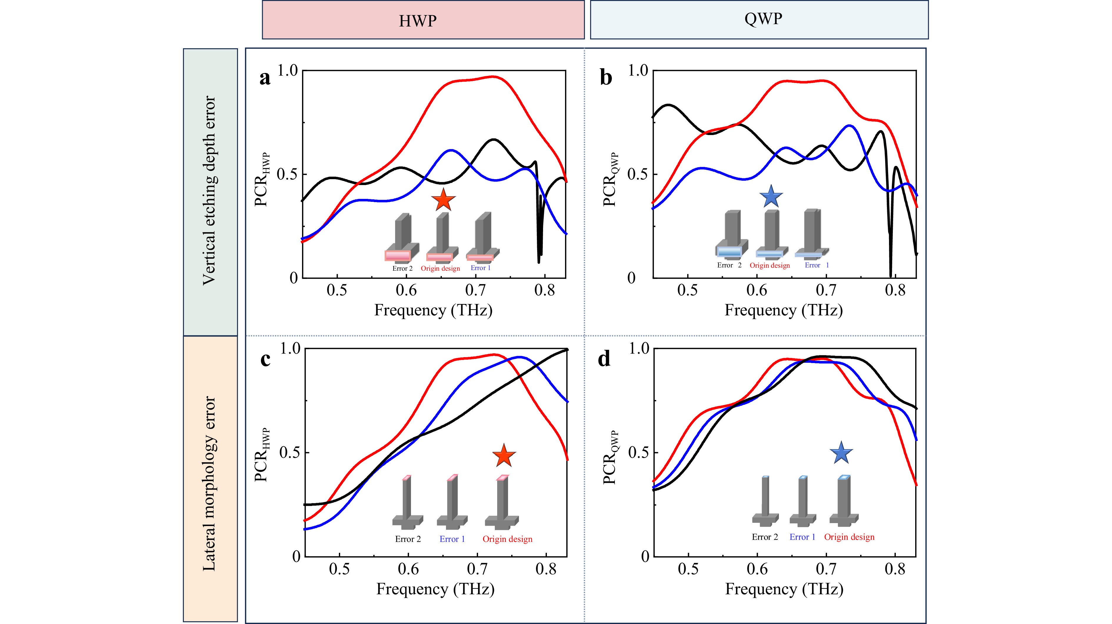
Fig. 3 Impact of structural imperfections on optical performance of the meta-device. a, b Calculated PCR spectra of the HWP and QWP of the original design parameters (red curve) and two different vertical etching depth errors ($ {h}_{1} $). In a and b, the black, blue, and red (original design) cures correspond to $ {h}_{1} $ values of 450 µm, 480 µm, and 510 µm in a and 450 µm, 480 µm, and 504 µm in b. c, d Calculated PCR spectra of the HWP and QWP of the original design parameters (red curve) and two different lateral morphology errors ($ l $ and $ w $). In c and d, $ {h}_{1} $ is fixed at 480 µm. The black, blue, and red (original design) curves correspond to the (l, w) values of (92.5 µm, 22.5 µm), (96 µm, 26 µm), and (100 µm, 30 µm) in c, and (73 µm, 48 µm), (77 µm, 52 µm), and (81 µm, 56 µm) in d, respectively. For all simulations, $ {h}_{3} $ is fixed at 62 µm.
Subsequently, we analyze how lateral morphology errors affect the performance of HWP and QWP. In our experiments, thick photoresists are often used as masking layers in the deep etching process of high AR dielectric structures to endure extended etching. However, thick photoresists typically contain a higher moisture content, which must be removed through baking before the etching process to prevent “resist popping” effect. This prebake operation will reduce the size of the etched pattern, ultimately leading to lateral morphology errors. Notably, such errors usually cause the etched patterns become smaller than the target design. To evaluate the influence of this issue, we employ FDTD simulations to obtain the PCR of the meta-devices (including HWPs and QWPs) with the same etching depth and different lateral dimensions (assuming a uniform reduction in length and width), as shown in Fig. 3c, d. The results show that reducing the lateral size significantly narrows the working bandwidth of the HWP. While the bandwidth of the QWP remains relatively stable, its spectral response exhibits a blue shift. This performance degradation is primarily due to the significant change in the phase difference $ \Delta \phi $ caused by the lateral size reduction, ultimately leading to a decrease in the device’s PCR (See more details in S5 and S6 of the Supplemental Material).
-
Based on our analysis of potential manufacturing errors, we develop an optimized fabrication technique to well address these fabrication challenges and successfully create the high AR silicon meta-devices with high working efficiency across a wide frequency band. All etching operations involve multiple etching and passivation steps during the Bosch process, which is a widely adopted dry etching technique. As illustrated in Fig. 4a, during the passivation step, a polymer layer is deposited to protect the sidewalls of the created microstructures. Next, the polymer at the bottom of the microstructures is rapidly removed to enable the following etching step, while the polymer on the sidewall remains for protecting lateral structures. By precisely controlling the balance between passivation and etching process, it is possible to construct the desired high AR patterns, as shown in Fig. 4b. During the passivation step, a protective polymer layer is deposited on the silicon surface and sidewalls through introducing C4F8 at a flow rate of 150 sccm for 2 seconds. This is followed by an auxiliary etching process (Etch 1), which is carried out by introducing SF6 at the flow rate of 200 sccm and applying a low-frequency (LF) power of 300 W for 1 second. The final step is longitudinal etching (Etch 2), maintaining the SF6 flow rate at 200 sccm and applying a LF Power of 60 W for 2 seconds. More detailed description of the key fabrication parameters is summarized in Supplemental Table S1.
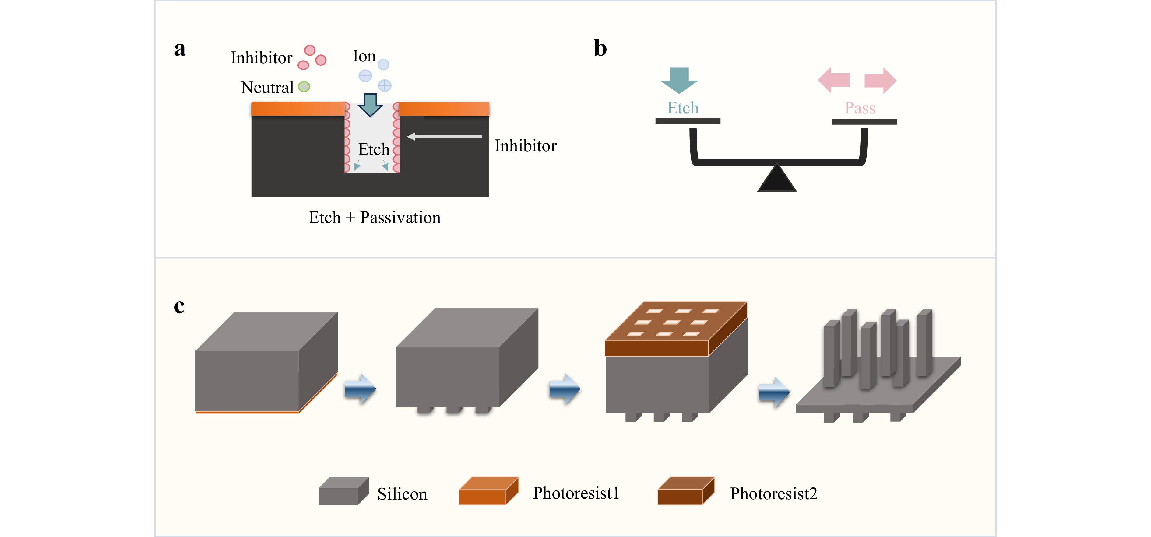
Fig. 4 Deep silicon etching via the Bosch process. a High AR anisotropic silicon etching is achieved by the repetitive alternation of etching and passivation steps. b The balance between etching and passivation is the key foundation to create high AR microstructures with steep sidewall while avoiding defects such as lateral etching or “black silicon”. c Flowchart of the fabrication process for our dielectric metasurfaces.
After that, we transfer the square shaped silicon microstructures (anti-reflection layer) and the backside alignment marks onto a pre-cleaned 600 µm silicon wafer using ultraviolet lithography firstly. The patterned wafer is then etched using an HSE M200 etcher. Subsequently, the high AR pattern is aligned and transferred via backside alignment lithography. The wafer undergoes a second etching process to form the high AR silicon pillar structures. After this process, we thoroughly clean the sample to remove any residual photoresist for subsequent testing. It is worth emphasizing that our optimized preparation process can reduce errors during preparation and also benefit our design engineering applications.
Photoresists are employed as the mask layer throughout all etch processes due to their high pattern resolution, substantial thickness tolerance, and ease of removal. It should be noted that in order to ensure the fabrication accuracy of the pattern, different mask layers need to be employed for various morphologies. For the anti-reflection layer, which requires relatively shallow etching, a thin layer of AZ5214 photoresist was proved to be sufficient for pattern transfer. While the large-feature shallow silicon structures are fabricated, each etching cycle removes approximately 1.03 $ \text{μm} $ of silicon. Thus, the 62 $ \text{μm} $ deep anti-reflection layer is successfully etched using about 60 cycles. The fabrication of high AR pillar meta-atoms requires a significantly larger etch depth. During the etching process, because the photoresist mask becomes progressively thinner, a thick resist (e.g., AZ4620) needs to be utilized as the mask layer. Before the deep etching process, the sample needs to be baked for pattern solidification. However, this will introduce a reduction in pattern dimension during fabrication, namely, a pattern shrinkage effect, which should not be overlooked and will affect the performance of the metasurfaces as analyzed in prior FDTD simulations (see Fig. 3c, d). This effect mainly originates from the evaporation of water in the photoresist during the baking process. To compensate for this effect, we intentionally increase the pattern length and width of the pattern during the design stage of mask according to our experience. This strategy effectively mitigates the fabrication-induced lateral deviations, allowing for the precise achievement of the target structural dimensions, as demonstrated in Fig. 5b, e. As a result, the repeatability and yield of the optimized fabrication have been significantly improved, effectively meeting the demands for highly robust device preparation.
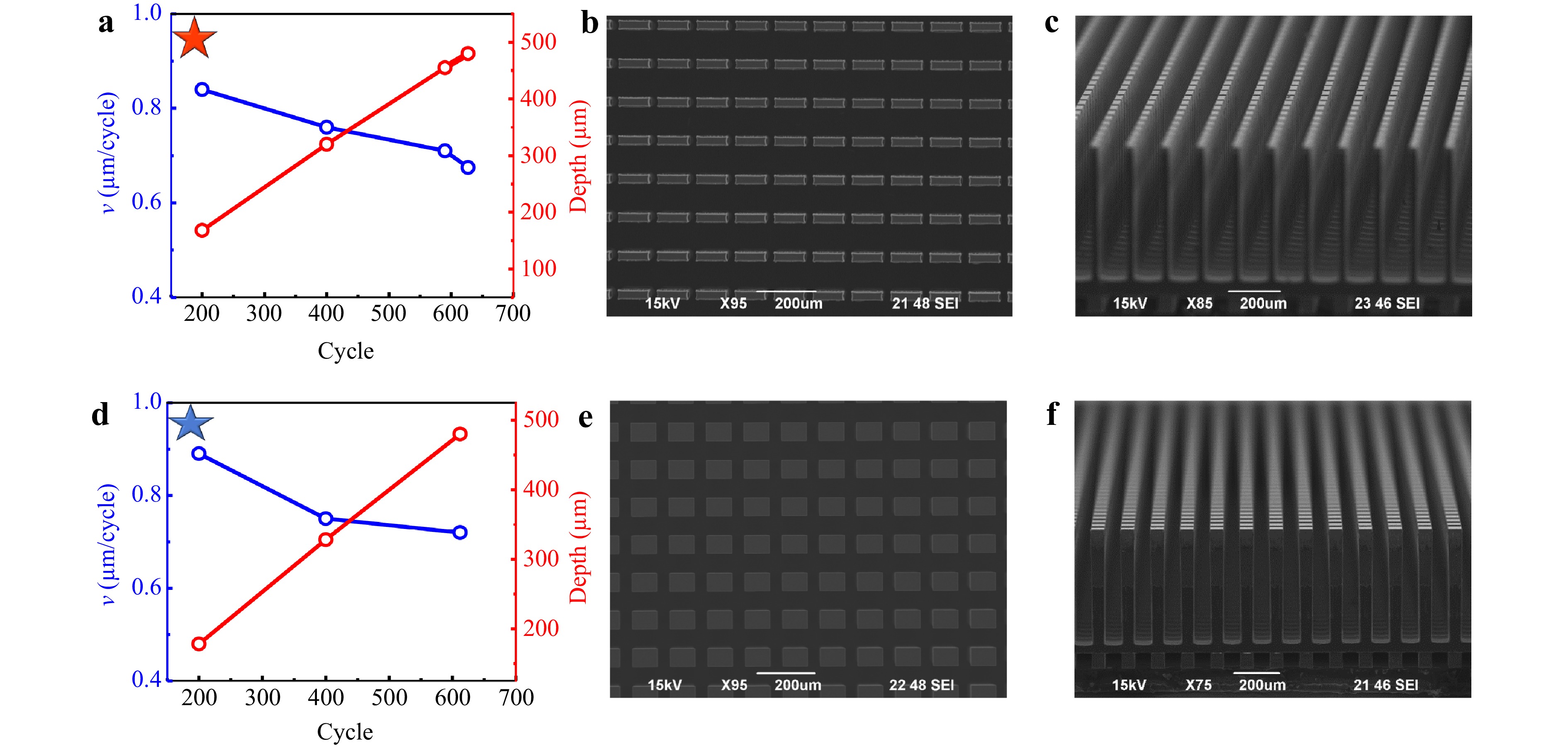
Fig. 5 Key fabrication conditions and scanning electron microscope (SEM) images of samples. a, d Etch rates and etching depth versus the cycle number for the high AR layer of HWP and QWP, respectively. Top-view (b, e) and side-view (c, f) SEM images of fabricated HWP (b, c) and QWP (e, f) samples.
Additionally, the etching depth is precisely controlled by etch rate and cycle count, which is critical for fabricating high-quality silicon meta-atoms (Fig. 3a, b). The etch rate for different pattern duty cycles is determined through the real-time monitoring of the etch depth, as shown in Fig. 5a, d. This approach enables precise control over etching depth, thereby minimizing errors induced by vertical non-uniformity. Throughout the etching process, the balance between etching and passivation cycles is carefully maintained, resulting in excellent sidewall verticality of the fabricated structures, as demonstrated in Fig. 5c, f.
-
To demonstrate the proposed design strategy and fabrication methodology, we characterize the polarization conversion performance of the fabricated meta-wave-plate samples based on a THz time-domain spectroscopy (TDS) system. Fig. 6a−c present the simulated and measured transmittance, transmission phase difference between two cross-polarization cases, and the corresponding PCR of the constructed HWP. The reference signal is obtained by replacing the meta-device by the open air and performing the similar measurement. The experimental results, showing excellent agreement with full-wave simulations, demonstrate that the HWP sample shows nearly unity transmittance, the phase difference of about π, and high PCR (PCR > 0.6) over a broad frequency range (0.6–0.8 THz, corresponding to a relative bandwidth of 28.57%). In addition, Fig. 6d−f show the simulated and measured transmission properties of the fabricated QWP, confirming the high polarization conversion performance (PCR > 0.6) across the target frequency band of 0.5–0.8 THz (relative bandwidth: 46.15%). Overall, the strong consistency between experimental and simulated results validates the effectiveness and reliability of our fabrication strategy in realizing high-performance THz meta-devices based on high AR silicon structures.
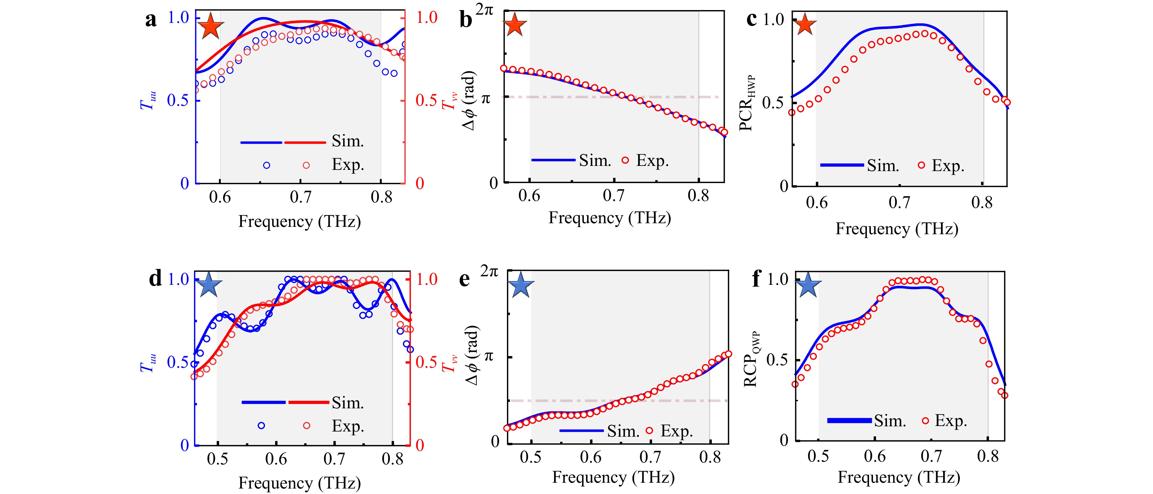
Fig. 6 Optical performance of the fabricated HWP and QWP. a Transmittance efficiency ($ {T}_{uu} $ and $ {T}_{vv} $), b transmittance phase difference ($ \Delta \phi $) and c PCR of HWP. d Transmittance efficiency ($ {T}_{uu} $ and $ {T}_{vv} $), e transmittance phase difference ($ \Delta \phi $) and f PCR of QWP. Measured data is shown in symbols, while simulation results are represented by solid lines.
-
The proposed design and fabrication methodology can also be applied to develop various high-efficiency functional meta-devices. For instance, we have designed and fabricated the flat metalens utilizing geometric phase mechanism, as illustrated in Fig. 7a. Based on the designed high-performance HWP as building blocks, we encode the following phase distribution inside the designed PB meta-device for the RCP light illumination case via simply tailoring the orientations of the meta-atoms at each local position:
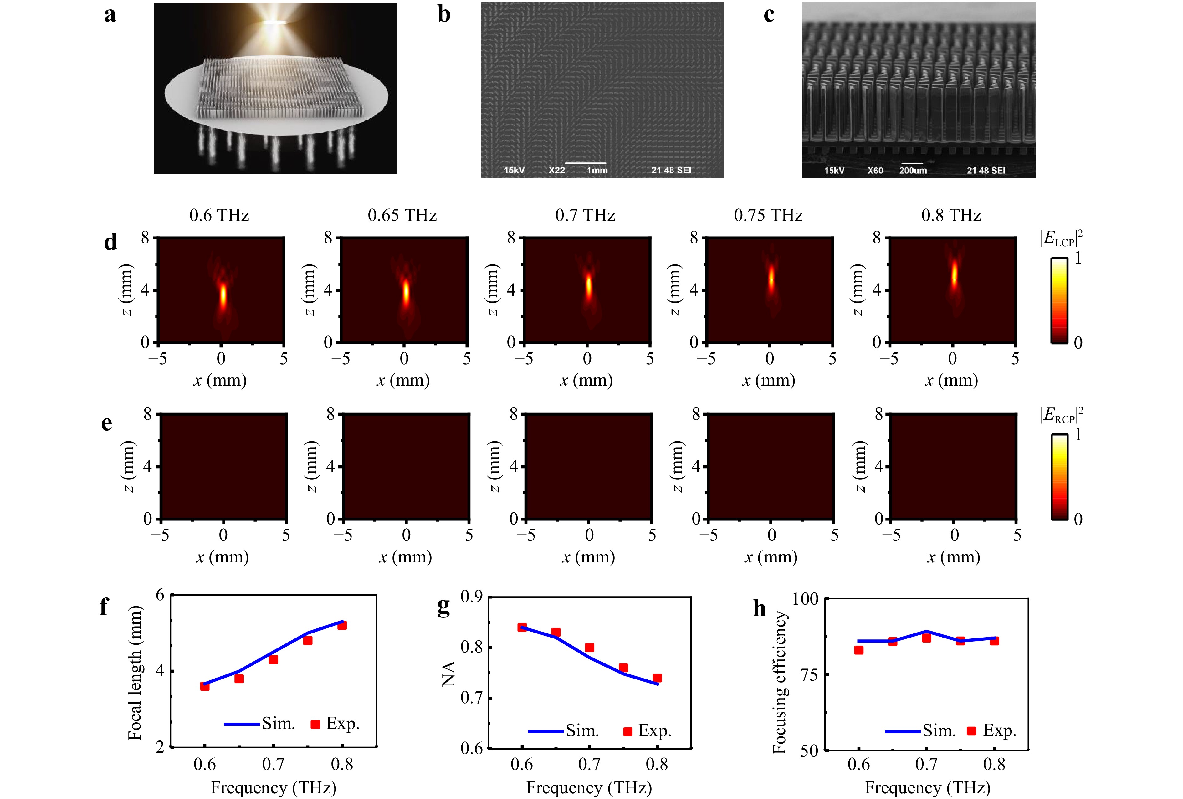
Fig. 7 Experimental characterization of the metalens. a Schematic illustration of the metalens. b, c Top-view and side-view SEM images of the fabricated sample. d, e Measured electric field intensity projected to LCP d and RCP e components in the xoz plane (y = 0 mm) of the metalens under RCP THz wave illumination with different frequencies. f−h Measured and simulated focal length f, NA g, and focusing efficiency h of the metalens as a function of frequency.
$$ \varphi \left(x,y\right)=-k\left(\sqrt{{x}^{2}+{y}^{2}+{F}^{2}}-F\right) $$ (4) where $ k $ is the wave vector of the light in free space, (x, y) denotes the position of the meta-atom on the metasurface, and $ F $ is the focal length ($ F=5~~~~\text{mm} $ at the central frequency of 0.7 THz).
The fabricated metalens sample with a total size of 10 × 10 mm2 is shown in Fig. 7b, c. Using a THz focal plane imaging system (see experimental setup in S7 of the Supplemental Material), we have measured the different components of the transmitted electric field distributions under the RCP illumination in the frequency range of 0.6–0.8 THz. Based on these data, we can retrieve the electric fields in the xoz plane carrying either LCP or RCP components, as presented in Fig. 7d, e. Clearly, the incident RCP beam is efficiently converted into LCP one focused in the pre-designed focal plane. Owing to the intrinsic dispersion nature of geometric phase, the focal spot gradually shifts away from the metalens as the frequency increases, corresponding to an increase in focal length and a decrease in NA, as shown in Fig. 7f, g.
Fig. 7h depicts the measured focusing efficiency of the fabricated metalens, which exceeds 85.56% across the entire operating bandwidth of 0.6–0.8 THz and reaches the highest value of 87% at 0.7 THz. Here, the focusing efficiency is defined as the ratio between the integrated power carried by the focal beam carrying the cross-polarization and that of transmitted THz beam. For comparison, full-wave simulation results show good agreement with experimental measurements (See detailed information in S8 of the Supplemental Material).
-
In summary, we have developed an optimized deep etching technique to construct high AR (about 19.2:1) dielectric THz meta-device with a high working efficiency across a wide THz frequency band. By systematically analyzing the influence of potential fabrication errors, we develop an optimized technique to effectively address these critical challenges, enabling the stable fabrication of high-quality silicon meta-device. As proof of concept, we successfully design and fabricate two dielectric meta-devices, i.e., an effective HWP and QWP. Both experimental measurements and full-wave simulations validate the high-efficiency polarization conversion effects across a broad target frequency band. The proposed THz meta-wave-plates exhibit superior comprehensive performances in terms of AR, absolute PCR and working bandwidth over the previous literatures57,61–65 (see Supplemental Table S2). Furthermore, by integrating the designed HWP with the concept of geometric phase, we have realized a high-efficiency and broadband THz metalens with an average focusing efficiency exceeding 85.56% in the frequency range of 0.6–0.8 THz. Compared to our previous work57, the fabrication technique has been significantly optimized, achieving enhanced reproducibility and quality in the production of high AR meta-devices. The meta-devices reported in this work exhibit substantially improved performance and the more diverse functionalities. This work not only demonstrates a viable strategy for the design and fabrication of high-performance THz meta-devices but also provides methodological insights into overcoming fabrication bottlenecks in deep etching technique. The proposed framework can be extended to a wide variety of THz meta-devices, paving the way for future applications in high-efficiency polarization control, THz imaging and sensing, wireless communications, and so on.
-
This work is supported by National Key Research and Development Program of China (Grant No. 2022YFA1404701), National Natural Science Foundation of China (Grant No. 12374344), and China Scholarship Council (202306890039). J.R. acknowledges the National Research Foundation (NRF) grant (RS-2024-00356928) funded by the Ministry of Science and ICT (MSIT) of the Korean government. We acknowledge technical support from Fudan Nanofabrication Laboratory for sample fabrications.
High aspect-ratio meta-device for broadband and high-efficiency terahertz wave manipulation
- Light: Advanced Manufacturing , Article number: 70 (2026)
- Received: 13 October 2025
- Revised: 12 April 2026
- Accepted: 19 April 2026 Published online: 23 September 2026
doi: https://doi.org/10.37188/lam.2026.070
Abstract: Efficient terahertz (THz) wave manipulation is essential for advancing communications, imaging, and security detection. However, conventional THz devices based on natural materials suffer from the issues of bulky size, low efficiency, and narrow bandwidth. Although dielectric metasurfaces offer a promising alternative, their practical applications still face challenges in high-precision manufacturing, particularly for structures with high aspect-ratio (AR) and deep etching depth. Herein, we experimentally construct high-quality silicon meta-devices for THz wave-controls. Guided by the analysis of the potential structural imperfections, we propose an optimized fabrication method based on the Bosch etching technology to address these challenges and create silicon meta-atoms with high AR and vertical sidewall. As a proof-of-concept, we design and fabricate a half-wave plate (HWP) and a quarter-wave plate (QWP) with a maximum AR of 19.2:1 and broad working bands (0.6–0.8 THz and 0.5–0.8 THz). Their polarization conversion ratios (PCRs) can reach 0.915 and 0.99 at approximately 0.73 THz and 0.66 THz, respectively. Furthermore, we experimentally realize a highly efficient and broadband metalens exhibiting the high average focusing efficiency of 85.56% within 0.6–0.8 THz. Our fabrication methodology can be extended to fabricate other high-performance metasurfaces, opening new possibilities for broadband THz applications.
Rights and permissions
Open Access This article is licensed under a Creative Commons Attribution 4.0 International License, which permits use, sharing, adaptation, distribution and reproduction in any medium or format, as long as you give appropriate credit to the original author(s) and the source, provide a link to the Creative Commons license, and indicate if changes were made. The images or other third party material in this article are included in the article′s Creative Commons license, unless indicated otherwise in a credit line to the material. If material is not included in the article′s Creative Commons license and your intended use is not permitted by statutory regulation or exceeds the permitted use, you will need to obtain permission directly from the copyright holder. To view a copy of this license, visit http://creativecommons.org/licenses/by/4.0/.

 DownLoad: