






-
Metallic wire-grid polarizers are effective optical devices for manipulating the polarisation state of light1, 2. They consist of a periodic array of parallel conductive wires on a substrate, allowing them to filter out one polarisation of light while transmitting or reflecting the other. When light is incident on a wire grid, the electric-field component that aligns with the wires ($ y $-polarisation) induces electron oscillations in the wires, which absorb and re-emit the energy of the light, thereby absorbing or reflecting it. In contrast, the electric field component perpendicular to the wires ($ x $-polarisation) interacts weakly with the electrons in the wires, resulting in most of it being transmitted. These polarisers are effective across a broad spectrum, ranging from ultraviolet to infrared. From the viewpoint of macroscopic electrodynamics, the wire-grid structure creates an effective anisotropic medium with in-plane anisotropy, meaning it interacts differently with different polarisations of light. Therefore, such a structure should have different transmission coefficients in $ x $- and $ y $-polarisations of the incident light, due to reduced symmetry. Consequently, an all-dielectric wire-grid polarizer can be designed for both orthogonal and linear polarisation. To avoid diffraction scattering, the pitch size of the wire grid should be less than the wavelength of light in the substrate, meaning that wire-grid polarizers operate in the metasurface regime.
One of the most interesting and promising approaches to enhancing metasurfaces and other photonic structures is to fabricate them using phase-change materials3−14. Because of the coexistence of two-phase states under normal conditions, these materials can provide a platform for on-demand control over the optical characteristics of metasurfaces.
In particular, metasurfaces based on phase-change materials have emerged as a promising platform for the design of wire-grid polarisers with dynamically modulating properties. For instance, Walther et al. presented a VO2-on-silica polariser that is switchable in the NIR and maintains its polarising function in both states, achieving an extinction ratio of 15 dB and requiring thermal actuation for switching15. In contrast, another VO2-based device on a silicon platform operated in the MIR region but functioned as a polariser in only one of its two states, achieving a lower extinction ratio of 6 dB, which can be thermally switched on and off16.
Another important phase-change material for metasurfaces is the germanium-tellurium-antimony alloy Ge2Sb2Te5 (GST), which has been widely used in rewritable data storage and electrical memories17, 18. In comparison with VO2, one of the GST phase states (i.e., the amorphous state) is almost transparent at the telecommunication wavelength of 1,550 nm. Because of its nonvolatile switching behavior and the large optical contrast between amorphous and crystalline GST phases in the visible and infrared ranges, GST thin films and metasurfaces have attracted considerable attention in photonics19−28. In the literature, GST-based research prototypes, including reflective displays29, electro-optical modulators30,31, active antennas32, 33, thermal camouflage34, hologram elements35, wave plates36, neuromorphic computing37, 38, and non-volatile memory39, have been recently demonstrated.
Recently, Lai et al. explored the use of GST on a mica substrate for wire-grid polarisers operating in the terahertz (THz) regime, demonstrating voltage-switchable operation40. This device acts as a polariser in a single state, highlighting the common trade-off between switchability and performance across the device’s phase states.
In this study, we leverage the phase-change properties of GST and combine them with the in-plane shape anisotropy of one-dimensional metasurfaces to design a switchable polarisation filter. In the following, we design a GST metasurface that, at telecommunication wavelengths, transmits light polarised parallel (to the wires) in the amorphous GST state and perpendicular to the wires in the crystalline state. To the best of our knowledge, such designs have not been reported previously. We will also study the stability of the designed metasurface with respect to variations in wavelength and angle of incidence, as well as geometrical parameters of the metasurface. We verify the concept of the switchable polariser by measuring the transmission characteristics of a fabricated GST metasurface produced using magnetron sputtering on a glass substrate.
A schematic of the GST wire-grid polarizer is shown in Fig. 1. It consists of a periodic array of parallel GST stripes (wires) with height $ h $ and width $ w $ on a glass substrate; the grating period is denoted by $ a $. As stated in the Introduction, owing to the in-plane anisotropy of the metasurface, the transmission coefficient of normally incident light differs in $ x $- and $ y $-polarisations for both phase states of GST. We characterise the ability of this GST metasurface to filter different linear polarisations in the amorphous and crystalline GST states by the overall polarisation efficiency $ f $ defined as
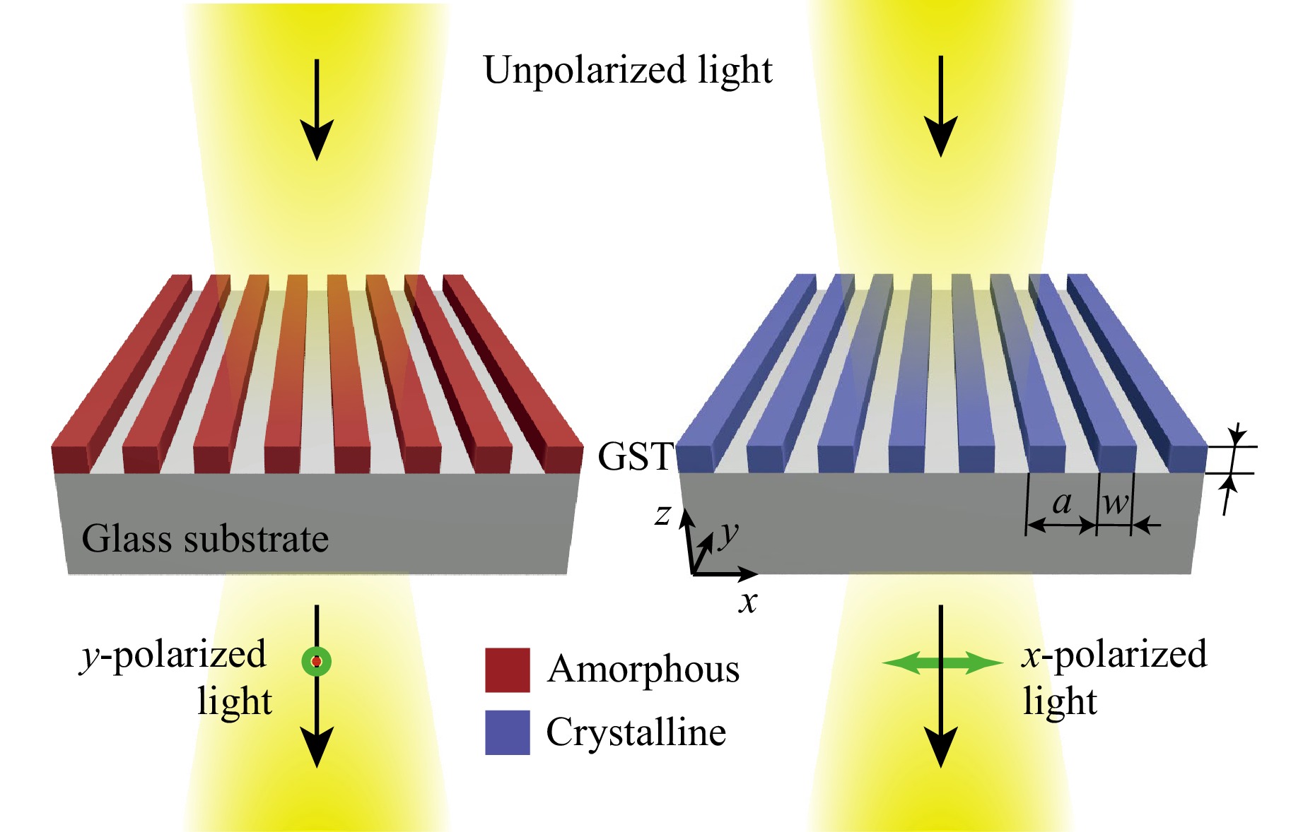
Fig. 1 A sketch of the metasurface, consisting of a z-uniform one-dimensional periodic GST layer on the glass substrate. In simulations, we also assume that there is a 20-nm-thick capping silica layer on the top of the GST stripes and at the bottom of air voids.
$$ f = -f_{\mathrm{am}}f_{\mathrm{cr}} = - \frac{T_x^\mathrm{am}-T_y^\mathrm{am}}{T_x^\mathrm{am}+T_y^\mathrm{am}}\cdot\frac{T_x^\mathrm{cr}-T_y^\mathrm{cr}}{T_x^\mathrm{cr}+T_y^\mathrm{cr}} $$ (1) which is the product of the polarisation efficiencies in the amorphous and crystalline states. In Eq. 1, $ T_{x}^\mathrm{am} $, $ T_{y}^\mathrm{am} $, $ T_{x}^\mathrm{cr} $, and $ T_{y}^\mathrm{cr} $ are the transmission coefficients of the structure in the amorphous and crystalline states of GST, while $ f_\mathrm{am} $ and $ f_\mathrm{cr} $ are the corresponding extinction ratios. The overall polarisation efficiency defined by formula (1) can be expressed in terms of the extinction ratios of the GST polariser in the amorphous and crystalline states, $ r_\mathrm{am} $ and $ r_\mathrm{cr} $, as follows:
$$ f = \frac{1-r_\mathrm{am}}{1+r_\mathrm{am}}\cdot\frac{1-r_\mathrm{cr}}{1+r_\mathrm{cr}} $$ (2) where
$$ r_\mathrm{am} = \frac{T_y^\mathrm{am}}{T_x^\mathrm{am}}, \; \; \; \; \; \; \; r_\mathrm{cr} = \frac{T_x^\mathrm{cr}}{T_y^\mathrm{cr}} $$ (3) According to the definition in (1), the overall polarisation efficiency $ f $ describes the behaviour of the GST grating as a switchable polariser; the closer $ f $ is to 1, the better the overall performance of the grating.
We used a genetic algorithm optimisation to determine the maximum overall polarisation efficiency for $ \lambda = 1,550 $ nm. To determine the optimal geometrical configuration using the figure of merit set in Eq. 1, it should be noted that the crystalline state of GST is highly absorbing ($ \mathrm{Im}\varepsilon \approx 10 $ at $ \lambda = 1.55 $ µm). Because of this material limitation, an ideal switchable polariser with $ T^\mathrm{am}_{x} = T^\mathrm{cr}_y = 1 $ and $ T^\mathrm{am}_y = T^\mathrm{cr}_x = 0 $ is unattainable. Furthermore, the overall polarisation efficiencies $ f_\mathrm{am} $ and $ f_\mathrm{cr} $ in Eq. 1 can yield high values due to a small denominator, even without a significant difference in the numerator (i.e., without a strong polarisation effect). To prevent this, we imposed a constraint on the minimum allowable transmission coefficient of $ T = $ 0.4 for a configuration to be considered efficient. The specific cut-off value (0.4) was determined through numerical optimisation with various constraints. A significantly higher cut-off would make it impossible to find a geometry that meets all the performance requirements, given the absorption of the material.
For the calculations, the dielectric permittivities of GST in the amorphous and crystalline phase states, $ \varepsilon_\mathrm{am} $ and $ \varepsilon_\mathrm{cr} $, respectively, were obtained from ellipsometry measurements (see Fig. 2). The optimised parameters of the metasurface are as follows: $ a = 560 $ nm, $ h = 285 $ nm, and $ w = 325 $ nm.
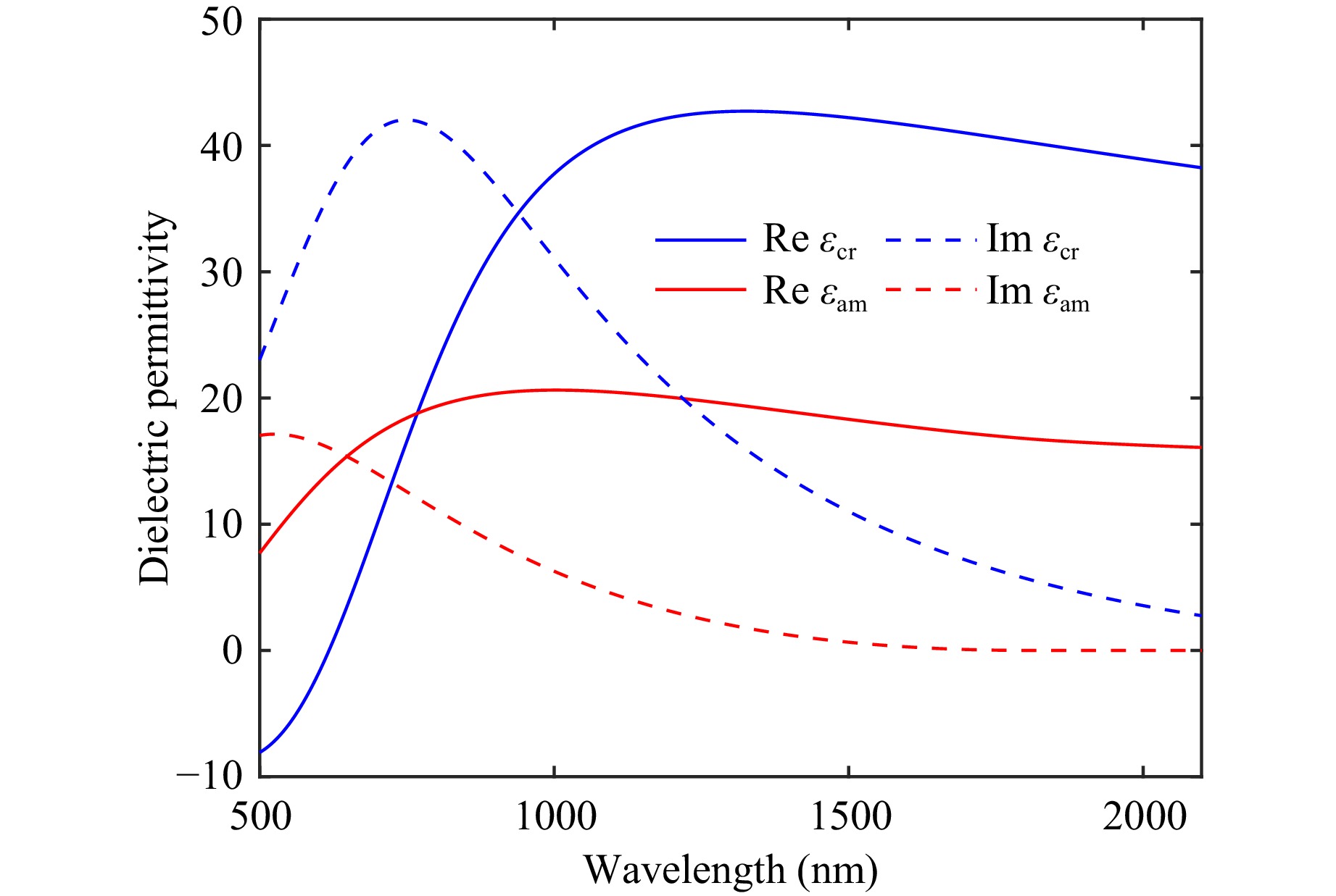
Fig. 2 Dielectric permittivity of GST in crystalline and amorphous states.
The transmission spectra of the metasurface with optimised geometrical parameters are shown in Fig. 3a for different polarisations and GST phase states. From Fig. 3a it can be seen that, in the wavelength range between 1,520 and 1,580 nm, the transmission coefficients in $ x $-polarisation in the amorphous state and in $ y $-polarisation in the crystalline states are almost zero, while the transmission coefficients in the opposite linear polarisation are above 0.25. The resulting overall polarisation efficiency was $ f\approx $ 0.92 at $ \lambda = $ 1,550 nm.
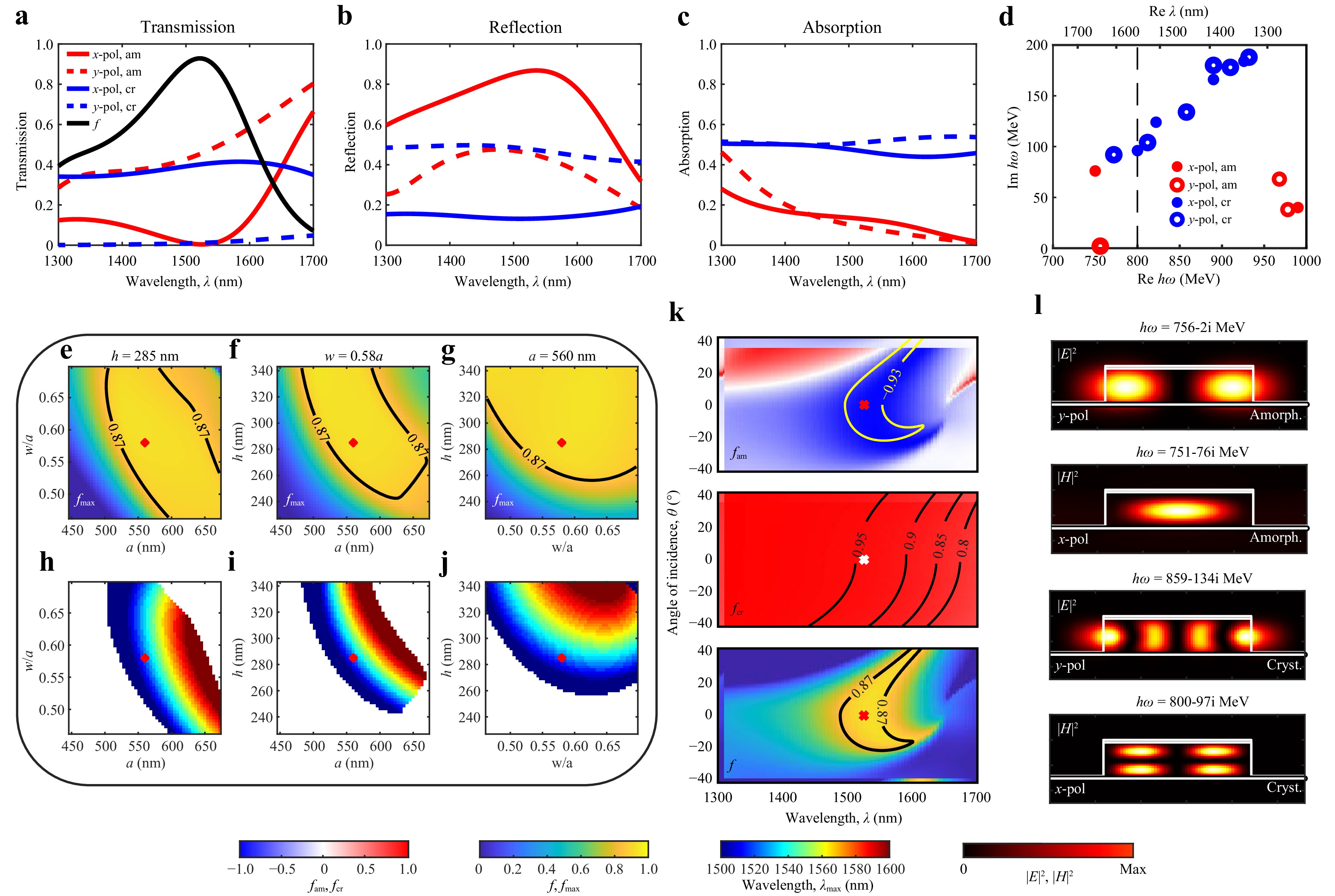
Fig. 3 a-c The calculated transmission, reflection and absorption spectra of the metasurface in $ x $- and $ y $-polarisations in crystalline and amorphous phase states of GST. d Position of the grating's eigenmodes on the complex energy plane. e-g The colormaps of a maximal overall polarisation efficiency $ f_{\max} $ of the metasurface falling within the wavelength range 1,500–1,600 nm as a function of the parameters $ a $, $ h $ and $ w $. h-j The colormaps of the wavelength of maximal overall polarisation efficiency, $ \lambda_{\max} $ calculated within the regions where $ f_{\max}>0.9 $. k The calculated polarisation efficiencies in amorphous and crystalline GST states and the overall polarisation efficiency of the metasurface as a function of wavelength and incident angle. Positive angles correspond to the $ xz $ incident plane, while negative angles correspond to the $ yz $ incident plane. The black solid lines in panels e-g, k denote the contour lines. The red and white cross in panels d-k denotes the optimal configuration. l Electric and magnetic field distribution in the grating's eigenmodes. The spectral features are governed by Mie resonances, and the data demonstrate consistent polarisation performance and robustness to geometric variations.
An important property of the designed metasurface is that it retains its filtering characteristics over a wide range of incident angles,measured from the normal to the sample surface. Fig. 3k shows calculated polarisation efficiencies in the amorphous and crystalline states, along with the overall polarisation efficiency, as a function of the wavelength and incident angle. From Fig. 3k, one can see that at $ \lambda = 1,550 $ nm, the overall polarisation efficiency exceeds $ f = $ 0.87 for incident angles up to 12° from normal. The high-$ f $-bandwidth is mostly constrained by the properties of the GST grating in the amorphous state, whereas in the crystalline state, the GST grating functions as a polariser over a wide range of wavelengths and incident angles. This suggests that the developed wire-grid polariser can operate not only for a normally incident plane wave but also for a Gaussian beam focused on the metasurface region by a lens with a numerical aperture of up to $ \sin 12^\circ \approx 0.21 $ (see the Supplementary Materials for the simulation of the propagation of a Gaussian beam through the designed grating).
Another remarkable feature of the wire-grid polarizer is its stability with respect to geometrical fabrication errors. To demonstrate this, in Fig. 3e-j we plot colormaps of the spectral maximum of the overall polarisation efficiency, $ f_{\max} $, as functions of two parameters among $ a $, $ w $, and $ h $. One can see that there is a broad region in which $ f_{\max} $ exceeds 0.87. In Fig. 3h-j, the wavelengths $ \lambda_{\max} $, at which the maximum overall polarisation efficiency $ f = f_{\max} $ is achieved, are shown by the colour variation from blue to red. Collectively, Fig. 3e-j demonstrates that, across a wide range of geometric parameters, the designed GST grating is characterised by an overall polarisation efficiency exceeding 0.87 at a wavelength—if not specifically at $ 1,550 $ nm, then within the range of 1,500 to 1,600 nm. From Fig. 3e-g, we can estimate the tolerable error for GST thickness as $ \Delta h = \pm30 $ nm, for GST stripe width as $ \Delta w = \pm0.06a \approx \pm24 $ nm, and for the period as $ \Delta a = \pm 80 $ nm. As shown in the Supplementary Materials, despite the variations of the peak wavelength with geometric parameters, the transmission coefficients $ T_y^\mathrm{am} $ and $ T_x^\mathrm{cr} $ are greater than $ \sim0.40 $ throughout the region $ f_{\max}>0.87 $.
To identify the physical mechanism responsible for the different polarisation states of transmitted light in the amorphous and crystalline GST states, we plot the reflection and absorption spectra of the designed metasurface (Fig. 3b, c). The absorption coefficients for the crystalline GST grating are higher than those for the amorphous grating, which aligns with the dispersions of $ \mathrm{Im}\; \varepsilon_\mathrm{cr} $ and $ \mathrm{Im}\; \varepsilon_\mathrm{am} $ shown in Fig. 2. The absorption spectra are almost identical for both incident light polarisations, whereas the reflection spectra differ significantly. This suggests that the polarisation-filtering effect in the transmission mode is mainly related to the polarisation effects in the reflection mode. To understand these effects, we determine the system's eigenmodes (Fig. 3d, l). The GST stripes exhibit Mie resonances, and the number of these resonances in the vicinity of the target wavelength is relatively large. Given the one-dimensional nature of the grating, the modes are either $ x $-polarised or $ y $-polarised with the magnetic or electric vector parallel to the stripes. The large imaginary parts of the resonances' eigenenergy, caused by absorption losses in the GST grating, make this system stable with respect to variations in geometry, wavelength, and incident angle. Thus, we conclude that the physical mechanism for filtering linearly polarised light arises from the interplay between electric and magnetic Mie resonances.
By inspecting the spectral positions and imaginary parts of the mode frequencies (Fig. 3d), one can elaborate on the robustness of the proposed device to non-ideal geometry. In the crystalline state, robustness is provided by low-Q modes originating from the high absorption of the material, which suppresses resonant effects and reduces sensitivity to geometrical variations. Conversely, in the amorphous state, robustness is achieved because the mode nearest to the target wavelength of 1.5 µm is located at $ \lambda = 1.65 $ µm. This indicates that the polarising functionality arises from the broadband interaction of this remote resonance with the background, rather than from a precise, high-Q mode, resulting in performance that is tolerant of fabrication imperfections. Notably, the low-Q factor in the crystalline state and the remoteness of modes in the amorphous state do not exclude useful performance; the theoretical transmission at the polarising condition remains around 0.4 in both GST phase states.
Subsequently, we fabricated three samples of GST stripes on a glass substrate to experimentally verify the feasibility of creating a switchable wire-grid polariser. The fabrication procedure involved DC magnetron sputtering to deposit an amorphous GST film on a glass substrate, followed by electron beam lithography and reactive ion etching to create a periodic surface structure. Crystallisation of the as-deposited sample with an amorphous thin GST film was performed at 250°C. See the Appendix for details on the deposition, lithography, and crystallisation processes. The SEM image of fabricated Sample 3 is shown in Fig. 4a, while the geometric parameters of the three fabricated samples are presented in Table 1. Note that there are some discrepancies between the geometric parameters of the fabricated samples and those of the optimised samples.
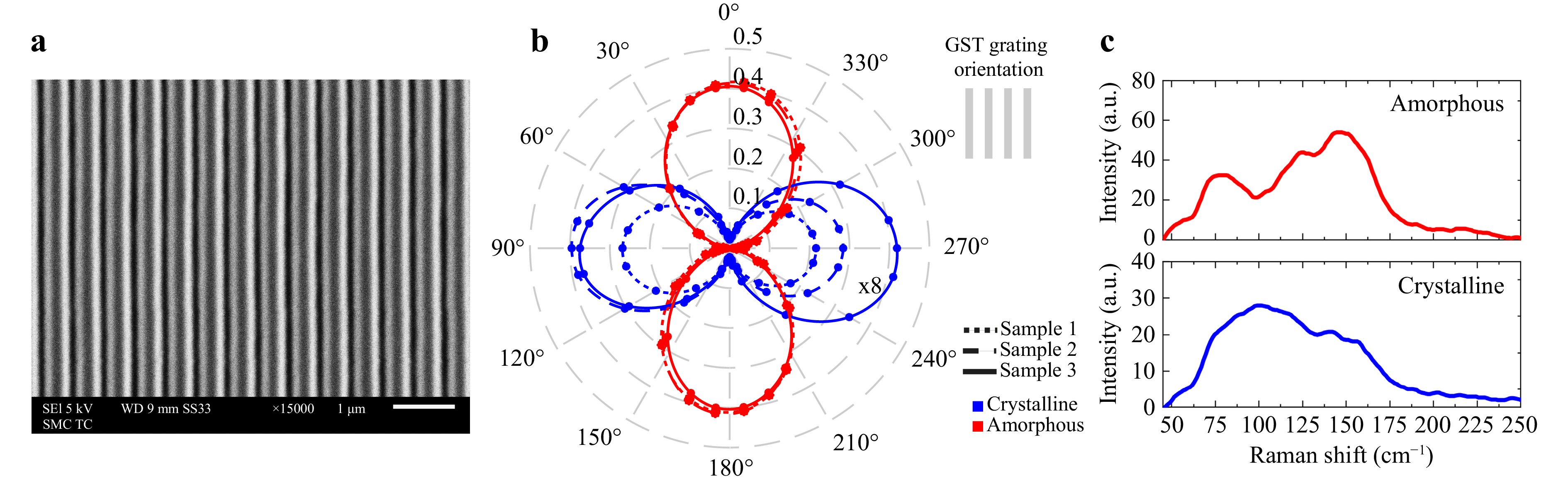
Fig. 4 a SEM image of the GST grating in Sample 3. b Experimental transmission as a function of the angle between the polarisation plane of incident light and GST stripes measured for crystalline (blue lines) and amorphous (red lines) states of samples 1, 2, and 3 (dotted, dashed, and solid lines). c Raman spectra from the as-deposited (amorphous) and annealed (crystalline) GST samples. b Panel illustrates the polarising behaviour of the GST wire-grid polariser in both its amorphous and crystalline states. The distinct difference between the two spectra in panel c confirms the presence of both the amorphous and crystalline phases.
Sample 1 a = 449 ± 15 nm, w = 391 ± 20 nm, h = 365 ± 10 nm experiment am. GST Tx 0.033 ± 0.015 Ty 0.413 ± 0.015 fam −0.852 ± 0.062 ram 10.97 ± 1.98 dB cr. GST Tx 0.03 ± 0.006 Ty 0.003 ± 0.0001 fcr 0.818 ± 0.034 rcr 10.0 ± 0.88 dB f 0.697 ± 0.058 Sample 2 a = 472 ± 20 nm, w = 408 ± 20 nm, h = 360 ± 10 nm experiment am. GST Tx 0.015 ± 0.007 Ty 0.414 ± 0.007 fam −0.930 ± 0.036 ram 14.41 ± 2.32 dB cr. GST Tx 0.043 ± 0.01 Ty 0.003 ± 0.0001 fcr 0.87 ± 0.03 rcr 11.56 ± 1.02 dB f 0.809 ± 0.042 Sample 3 a = 502 ± 14 nm, w = 418 ± 20 nm, h = 360 ± 10 nm experiment am. GST Tx 0.005 ± 0.001 Ty 0.405 ± 0.014 fam −0.976 ± 0.005 ram 19.08 ± 0.88 dB cr. GST Tx 0.05 ± 0.004 Ty 0.003 ± 0.005 fcr 0.89 ± 0.18 rcr 12.2 ± 7.3 dB f 0.869 ± 0.176 Table 1. Experimental results for fabricated Samples 1–3. Polarisation efficiencies $ f_\mathrm{am} $, $ f_\mathrm{cr} $ and $ f $ are calculated using formula (1), while extinction ratios $ r_\mathrm{am} $ and $ r_\mathrm{cr} $ are calculated using formula (3).
To confirm that the samples were in amorphous and crystalline states, we measured the Raman spectra of the as-deposited and thermally annealed GST samples (Fig. 4c). As shown in Fig. 4c, thermal annealing strongly changes the shape of the Raman spectrum compared with the initial GST sample. The changes in the spectrum profile are in good agreement with previously reported data and with the characteristics of the phase transition from the amorphous to the metastable cubic crystalline GST phase41, 42. This confirms the phase transition of GST from an amorphous to a crystalline state after thermal annealing. In addition, we performed another crystallization/amorphization cycle to verify the reversibility of the phase-change process (see Fig. S4 in the supplementary Materials).
The fabricated samples were investigated by measuring the transmission of a linearly polarised laser beam with a wavelength $ \lambda = 1.55 $ µm (SFL1550P, Thorlabs) as a function of the angle between the polarisation plane and GST stripes. The power of the laser radiation incident on the sample was 3.8 mW, and the laser polarisation extinction ratio exceeded 25 dB.
The experimental transmission coefficients of Samples 1–3 are shown in Fig. 4b as a function of the angle between the GST stripes and the polarisation plane of the incident light, $ \alpha $. For an ideal polariser that completely blocks one of the two orthogonal linear polarisations, $ T(\alpha) $ dependence should follow the $ \cos^2{\alpha} $ rule. From Fig. 4b, it can be observed that despite some asymmetry in the transmission $ \alpha $-dependencies (owing to fabrication imperfections, structural anisotropy beyond the ideal design, and experimental misalignment), the polarisation of the transmitted light is almost linear in both GST states. In particular, for the amorphous phase of GST, the transmission coefficient reaches its maximum value ($ T\approx $ 41.5% for all three samples) when the polarisation plane was parallel to the stripes. In contrast, in the crystalline phase, the maximum transmission (approximately 5% for Sample 3) is achieved when the GST stripes and the incident polarisation plane are perpendicular to each other. Note that the transmission of only 5% in the crystalline state is not a limiting factor using the fabricated grating as a polarizer, because $ \cos^2{\alpha} $-like angular dependencies are observed with confidence. These observations indicate that, in the amorphous state, the samples behave as a polariser for $ y $-polarisation, whereas in the crystalline state, they behave as a polariser for $ x $-polarisation, as predicted theoretically. It should be noted that although the geometric parameters of the fabricated gratings differ from the optimal ones, the overall experimental polarisation efficiency and extinction ratios of the three samples remain relatively high; hence, the samples still function as switchable wire-grid polarisers (see Table 1). However, the transmission through the sample in the crystalline state is approximately eight times lower than that in the amorphous state. This feature is well reproduced in FMM simulations, taking into account errors in the determination of geometric parameters from SEM images and ellipsometry (see Table 1 for details).
The differences between theoretical predictions and experimental results primarily originate from three sources: i) sample imperfections, ii) uncertainty in the geometric parameters used in the simulations, and iii) the limited performance and sensitivity of the experimental setup. Errors due to sample imperfections arise from the non-ideal nature of the fabricated sample. Key factors include sidewall roughness, corner rounding, and material scattering losses owing to imperfections. These effects, which are challenging to model perfectly, lead to deviations in the measured optical response compared with idealised simulated structures. The uncertainty in the geometric parameters for the simulations is a consequence of the non-ideal nature of the sample. Small variations in the input dimensions affect the simulated optical properties, creating a range of possible theoretical outcomes. These geometry-related uncertainties are explicitly accounted for as error margins in the theoretical values presented in Table 1 (column "theory").
Furthermore, errors are also introduced by the experimental setup itself. Non-ideal positioning of the sample relative to the optical elements and the limited sensitivity of the detector contribute to the experimental error, which is indicated in Table 1, column "experiment". Such errors must also be considered when comparing theoretical and experimental results.
Crucially, when the theoretical predictions of the transmission coefficients are considered with their geometry-related errors and compared with their measured counterparts, including experimental setup errors, they are in agreement across all data. The polarisation efficiencies and extinction ratios do not always coincide because these quantities are calculated based on the parameters $ T^\mathrm{am,\; cr}_{x,y} $ with the above-mentioned errors. Nevertheless, the observed deviations for the parameters $ f_\mathrm{am,\; cr} $, $ r_\mathrm{am,\; cr} $, and $ f $ are not large compared with their mean values. This confirms that our model, although based on idealised assumptions, adequately captures the essential physics of the system.
A comparison of our wire-grid polariser with existing polarisers is summarised in Table 2. Based on this table, our polariser demonstrates a combination of features not found in existing devices. Although commercial polarisers from Thorlabs achieve higher extinction ratios, they lack switchability. Among switchable polarizers, our work distinguishes itself by maintaining polariser functionality in both states, unlike VO2-based devices15, 16 and GST-based THz polarisers40, which lose their polarisation capability in one state. Furthermore, our GST-on-glass platform offers reversible thermal switching within the telecommunications band (1.5−1.6 µm), achieving competitive extinction ratios of 10–14 dB while providing full polarisation control in both GST phase states.
Reference Material platform Switchable Polarizer in both states Range Bandwidth Extinction ratio Switching Thorlabs43 metal on glass no — VIS, NIR 0.3–3.2 µm 15–37 dB — Thorlabs44 metal on BaF2, CaF2, ZnSe no — MIR, FIR 2.5–30 µm > 22 dB — Thorlabs45 metal on silicon no — VIS, NIR 3–12 µm > 30 dB — Walther15 VO2 on silica yes yes NIR 1.2–1.6 µm ~15 dB temp. Lawandi16 VO2 on silicon yes no MIR 5–8 µm ~6 dB temp. Lai40 GST on mica yes no THz 0.1–2.5 THz ~12 dB voltage our work GST on glass yes yes NIR 1.5–1.6 µm 10–14 dB temp. Table 2. Comparison of the wire-grid polarizers.
We note that laser-based switching, while effective for proof-of-principle demonstration, is not the only approach available. Electrothermal switching via a resistive microheater integrated beneath the GST layer enables significantly faster operation, with switching times on the sub-microsecond timescale, as demonstrated for GST-based devices with bottom-heater configurations46.
In our device, electro-thermal switching can be achieved by integrating the metasurface with a thin-film external heater. This heater, fabricated from materials such as ITO or silicon, is transparent at a wavelength of 1,550 nm and possesses the required electrical conductivity. The switching mechanism relies on precise electrical pulses: weaker, longer pulses heat the amorphous GST to its crystallisation temperature (exceeding 160°C), whereas shorter, more powerful pulses raise the temperature to the melting point of the material (over 630°C) before rapid cooling re-amorphises it8. This general approach to electrical switching has been successfully demonstrated in previous studies46. Indium tin oxide (ITO) or polysilicon is a suitable choice for the heating layer because of their transparency in the relevant IR range. The feasibility of multiple switching cycles without GST degradation has been demonstrated using a doped silicon heater47. While changing the underlying heater material requires a recalculation of the lattice parameters to account for the shift in the effective refractive index, the fundamental geometry of the wire-grid polariser will remain the same.
We have designed a GST-based wire-grid polariser optimised for telecommunication wavelengths. The geometric parameters of the optimised polariser are stable against fabrication errors. The physical mechanism for the filtration of linearly polarised light is attributed to the combination of electric and magnetic Mie resonances. The operating wavelength can be adjusted by changing the geometry of the metasurface. We have verified the proposed concept by measuring the transmission spectra of a fabricated sample of a wire-grid metasurface. The highest overall experimental polarisation efficiency was $ f = $ 0.874. This study serves as a proof-of-principle demonstration of a dynamically switchable wire-grid polariser based on GST. The future realisation of practical devices will require additional steps, such as the integration of contact electrodes for efficient electrical switching. Because the phase transition in GST films can occur on a sub-microsecond timescale, the developed switchable wire-grid polariser provides significant potential for the creation of a fast and compact polarisation modulator at telecommunication wavelengths.
HTML
-
Electromagnetic simulations were performed using the Fourier modal method in the scattering matrix form48 (also known as rigorous coupled-wave analysis49). This method is based on splitting the structure into elementary planar layers that are homogeneous in the vertical direction and periodic in the horizontal direction(s). The solutions of Maxwell’s equations for each layer were obtained by decomposing the electric and magnetic fields into Floquet-Fourier modes (plane waves). The exact solution is represented as an infinite series of these modes. In numerical simulations, the scattering matrices are determined by considering a finite number of plane waves $ N_p $. The calculation accuracy increases with increasing Np; however, the calculation time is proportional to $ N_g^3 $. To improve convergence, we implemented Li’s factorisation rules50. Consequently, the total number of plane waves in our simulations was $ N_g = 101 $.
To ensure the feasibility of the geometry, we implemented the following constraints to guide the algorithm towards practical geometries: a) the period was constrained to avoid the excitation of diffraction orders, b) the grating height was limited to prevent issues with tilted sidewalls that can occur during the etching process of high-aspect-ratio structures, and c) the minimum wall thickness was set to a value that is resolvable with standard electron-beam lithography techniques. These constraints ensure that the optimised design is not only high-performing but also achievable with modern nanofabrication processes.
The fabrication procedure for the wire-grid polariser was as follows. The initial amorphous GST film was deposited via DC magnetron sputtering of a polycrystalline target at room temperature. During the process, the pressure of Ar+ ions was $ 5\cdot10^{-3} $ Torr, and the sputtering power was 25 W. An alkali-free boro-aluminosilicate glass (Corning Glass 1737F) with a thickness of 0.7 mm was used as the substrate. The thickness of the as-deposited GST film, as measured by atomic force microscopy, was approximately 310 nm. The surface roughness of the GST film, determined as the root-mean-square value of the height according to ISO 25178, was 0.56 ± 0.01 nm.
After spin-coating the electron beam resist ma-N 2403 at 4,000 rpm onto the glass substrate, it was baked at 90°C for 1 min. Electron beam lithography was performed using a 50 kV setup (CRESTEC CABL-9050C). The template file consisted of nine gratings with slightly different grating periods and filling factors. After electron-beam lithography, reactive-ion etching of GST was performed in a setup (Corial 200R) with an SF6/Ar gas mixture at a pressure of 5mTorr and an RF bias of 370 V. The etching process was controlled using a built-in thin-film interferometer. The electron beam resist was removed in the same setup using O2 plasma. To prevent oxidation of the fabricated structure, a 20-nm-thick silicon dioxide layer was deposited after lithography.
To switch the entire GST film into the crystalline phase for optical measurements, the samples were crystallized by annealing at 250°C for 30 min under an argon flow using a Linkam HFS600E-PB4. The heating and cooling rates were 5°C/min. The choice of annealing temperature was based on the X-ray diffraction results, which indicated that this temperature enables the crystallisation of amorphous GST thin films into the NaCl-type structure51. Thermal crystallisation was chosen to ensure complete and spatially uniform phase transformation across the grating area, eliminating the influence of temporal and spatial non-uniformity of heating inherent to laser radiation. Therefore, the thermally crystallised state was used to evaluate the maximum achievable optical contrast.
Reversible switching between amorphous and crystalline phases of GST was demonstrated experimentally using the DLW (direct laser writing) method. Amorphization and crystallisation were achieved by scanning the laser beam across the GST film, with a radiation wavelength of 1,030 nm, a pulse duration of 260 fs, and a pulse repetition rate of 10 Hz. The laser radiation was focused by a lens onto the sample, locally heating it and thereby inducing phase switching. The beam size was approximately 30 µm. High-precision three-axis stages allowed precise positioning of the GST film with respect to the focused laser beam, causing local heating and GST phase switching. Crystallisation and amorphization were performed at various fluences. The results of cyclic switching are illustrated with rectangular markers in Fig. S3c: thermal crystallisation of the initial amorphous sample (1st), laser-induced amorphisation (2nd and 4th), and laser-induced crystallisation (3rd). At a scanning speed of 200 µm/s, the switching time for the fabricated filters was several minutes.
The amorphous state of PCMs is subject to a time-dependent drift in the refractive index and extinction coefficient, driven by structural relaxation and a change in the optical bandgap52. However, this effect is strongly temperature-dependent. For reference, the total bandgap change reported for GST after annealing at 80°C for 27 h was only $ \sim23 $ meV (2.9%). This modest variation does not significantly affect polarisation-filtering performance. For characterisation, the sample was dismounted from the heating or cooling stand. At room temperature, the structural relaxation rate is orders of magnitude slower, and the optical parameters of both phases remain effectively constant over the timescales relevant to our measurements. To confirm this experimentally, optical measurements were repeated on different days, and no significant deviations in transmission or polarisation extinction ratio were observed between sessions.
The transmittance of light through the metasurfaces under study was measured using a linearly polarised SFL1550P laser source (Thorlabs) with a polarisation extinction coefficient of 25 dB (Fig. 5). Collimated laser radiation with a wavelength of 1,550 nm was directed at the sample, which was fixed on a holder that could be rotated at an arbitrary angle relative to the polarisation plane of the laser radiation. The laser power incident on the sample was 3.8 mW. The power of the radiation transmitted through the sample was measured using an S132C power detector (Thorlabs). The dependence of the transmitted power on the sample rotation angle was measured in the range of 0–360° in increments of 5–10°. Consequently, by normalising to the power incident on the sample, the angular dependence of light transmittance through the studied metasurfaces was obtained.
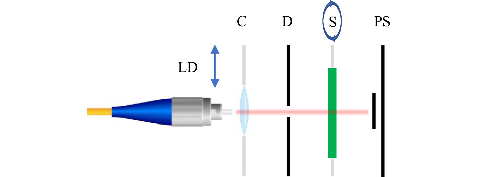
Fig. 5 Schematic of the experimental setup for measuring the dependence of the transmission coefficient on the angle of rotation of the sample relative to the plane of polarisation of the laser radiation: LD—output of the linearly polarised fiber-coupled laser diode (arrows indicate vertical polarisation of emitted light), C—collimator, D—diaphragm, S—rotating sample holder with metasurface under study (can be replaced with polariser P), PS—Ge photodiode power sensor. The initial sample position orientation—GST gratings are elongated along the vertical 0°–180° direction of the sample holder rotator—was always aligned with the plane of polarisation of the laser diode prior to each transmission measurement. To verify the laser diode polarisation plane orientation and the actual extinction coefficient, polariser P was placed instead of the sample. The corresponding angle dependence of the transmission coefficient confirmed both vertical orientation of the polarisation plane and ~26 dB polarisation extinction coefficient of the laser diode.
-
This work was supported by Russian Science Foundation grant No. 23-79-10309 (https://rscf.ru/en/project/23-79-10309/). GST thin films were deposited with contributions from the research laboratory “Materials and devices for active photonics” (FSMR-2025-0002). J.-K.S. was supported by the National Research Foundation of Korea (NRF) (RS-2026-25492742) and the ICT Creative Consilience Program (IITP-2020-0-01821) funded by the Ministry of Science and ICT, Korea. The authors acknowledge O. Klimenko for FTIR measurements and O. Kushchenko for fs-laser modification.

 DownLoad: