






-
Quantum dot light-emitting diodes (QLEDs) show considerable promise as an advanced technology for lighting and display applications with high brightness and excellent colour properties1–6. After years of effort, both the efficiency and brightness of QLED prototype devices have been greatly improved, approaching the industrial requirements7–10. A Micro-QLED is a promising microdisplay technology for augmented reality (AR) applications because of its high brightness and easily achievable high resolution11–21. Various fabrication processes have been successfully adapted for QLED prototypes, including spin-coating3,4, inkjet printing22,23, and blade-coating24–27. Considering the use of Micro-QLED for AR displays21,28–30, there is an urgent need to develop a wafer-scale fabrication process for high-resolution Micro-QLEDs with a pixel size smaller than 5 μm. In a previous study, we developed photolithography template-assisted processing to fabricate high-resolution Micro-QLED electroluminescent (EL) panels31. This process can potentially be combined with spin coating, or blade coating, or inkjet printing for the wafer-scale fabrication of Micro-QLEDs.
In previous studies, Micro-QLEDs have been fabricated through the inkjet printing32,33 and transfer printing15,34, and direct photolithography35,36 of quantum dots (QDs). To date, only a few studies have reported high-resolution EL devices, owing to limited processing compatibility and current leakage between QD patterns15-17,34,37-42. Compared with these fabrication processes, photolithography template-assisted processing is more compatible with industrial-scale photolithography technologies. During wafer-scale fabrication, the droplet spreading of the QD ink is a key step in solution processing43–45. Droplet spreading is a common challenge when using solution processing for the fabrication of large-area devices, such as perovskite light-emitting diodes46–50, perovskite solar cells51–53, and QLEDs24,26,27. To achieve the wafer-scale fabrication of Micro-QLEDs, we addressed the challenge posed by limited droplet spreading on the photolithography template.
In this study, we introduced a binary solvent of hexane and octane to address the challenge of limited droplet spreading during the spin-coating process, achieving a 2-inch wafer-scale area. In situ high-speed microscopic observations revealed the critical role of Marangoni flow in governing the motion direction of the three-phase contact line. We further designed a 2-inch wafer-scale fabrication process for micro-QLEDs and obtained 15 microdisplay panels of 0.46-inch Micro-QLEDs with a resolution of 2,510 pixels per inch (a pixel size of 4–50 μm). In addition, these Micro-QLED wafers had high external quantum efficiencies of 22.8%, 20.8%, and 1.4% for their red-, green-, and blue-emitting Micro-QLEDs, respectively, which are some of the highest reported performances for large-area devices.
-
Fig. 1a schematically shows the 2-inch wafer-scale fabrication process for the Micro-QLED device. First, a pre-patterned template was prepared on a 2-inch ITO substrate by photolithography template-assisted processing. Subsequently, the fabrication of the QLED was continued through the sequential spin-coating of successive functional layers on the template to obtain a Micro-QLED. Finally, the 2-inch Micro-QLED device was diced into a individual 0.46-inch microdisplay panels.
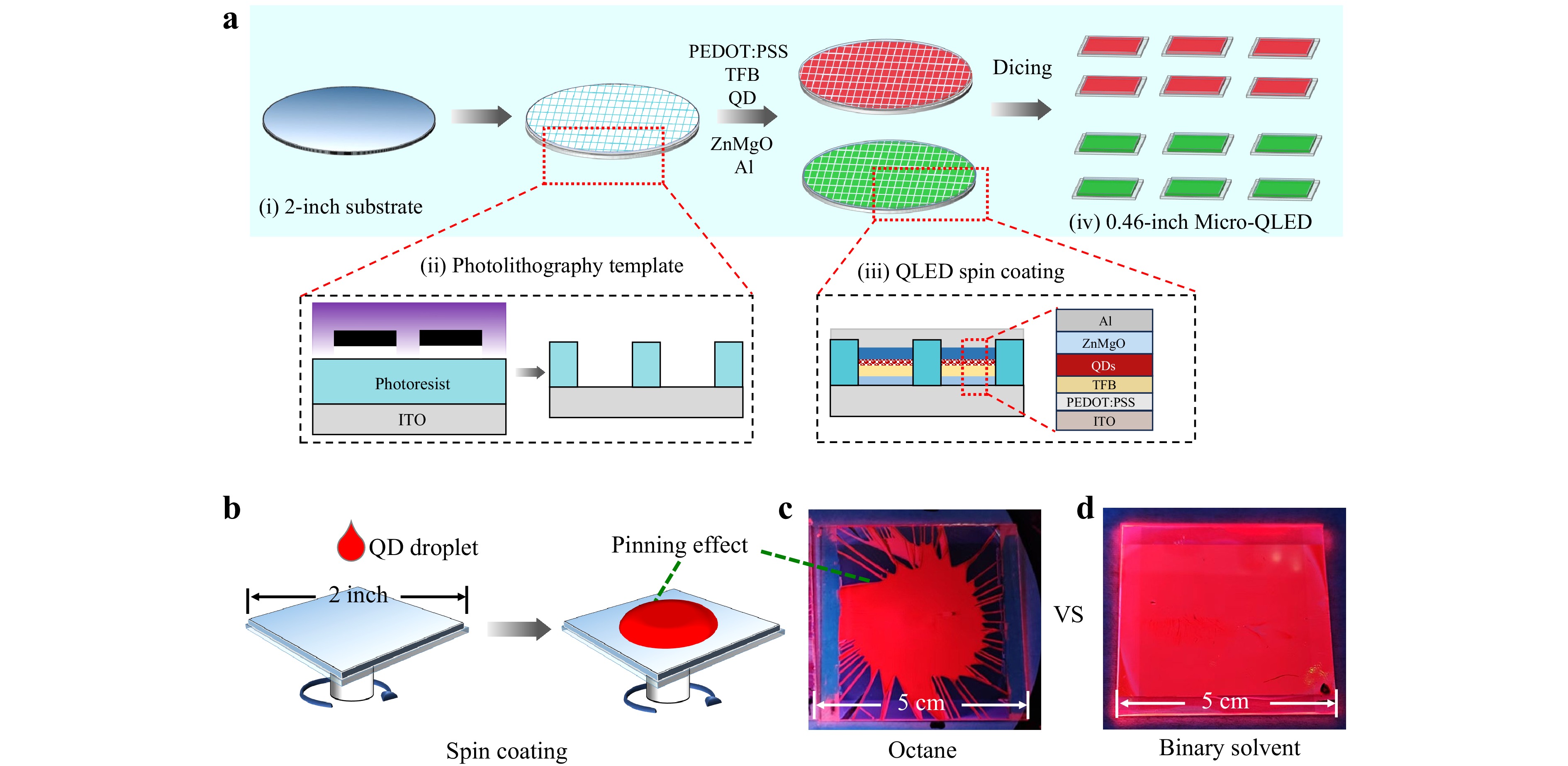
Fig. 1 Two-inch wafer-scale manufacture of Micro-QLED. a Schematic diagram of 2-inch wafer-scale manufacturing processing. b Schematic diagram of the spin-coating process using a QD ink droplet. c Photoluminescence image of a 2-inch substrate spin-coated by QD inks in octane. The volume of the QD droplet is 40 μL. d Photoluminescence image of a 2-inch substrate spin-coated by QD inks in binary solvent of hexane and octane. A volume of 40 μL was used for the QD droplets.
Based on our experience, the droplet spreading of QD ink is a common challenge in the large-area fabrication of solution-processed devices. As shown in Figs. 1b, c, interfacial instability of the droplet occurred during the spin-coating of the QD inks in octane on the 2-inch substrate because of the pinning effect of the three-phase contact line. The problem posed by the limited spreading area could be successfully addressed using QD inks in a binary solvent of hexane and octane (Fig. 1d).
The dynamics of film formation using QD inks were investigated by in situ microscopy. Fig. 2a, b compare the film formation processes of the QD inks in octane and the binary solvent. When using the octane system, the droplet underwent a slow-spreading process, in which the spreading of a 0.2 μL droplet lasted for 5 s. In the binary solvent system, the droplet underwent a fast-spreading process, in which the spreading of a 0.2 μL droplet also lasted for 5 s. However, the calculated spreading area when using binary solvent was 11 mm2, of approximately 3 times larger than that when using the octane system (4.3 mm2) (Fig. S2). The film formation of the droplets include two stages: spreading (< 5 s) and drying (> 5 s) (Fig. 2c). The spreading stage was the key step in determining the final droplet spreading area of the QD ink54. In this stage, the surface tension gradient induced by solvent evaporation could trigger a Marangoni flow. Together with the capillary flow driven by the non-uniform evaporation flux across the droplet surface, these coupled flows govern the motion dynamics of the three-phase contact line, thereby affecting the final spread area.
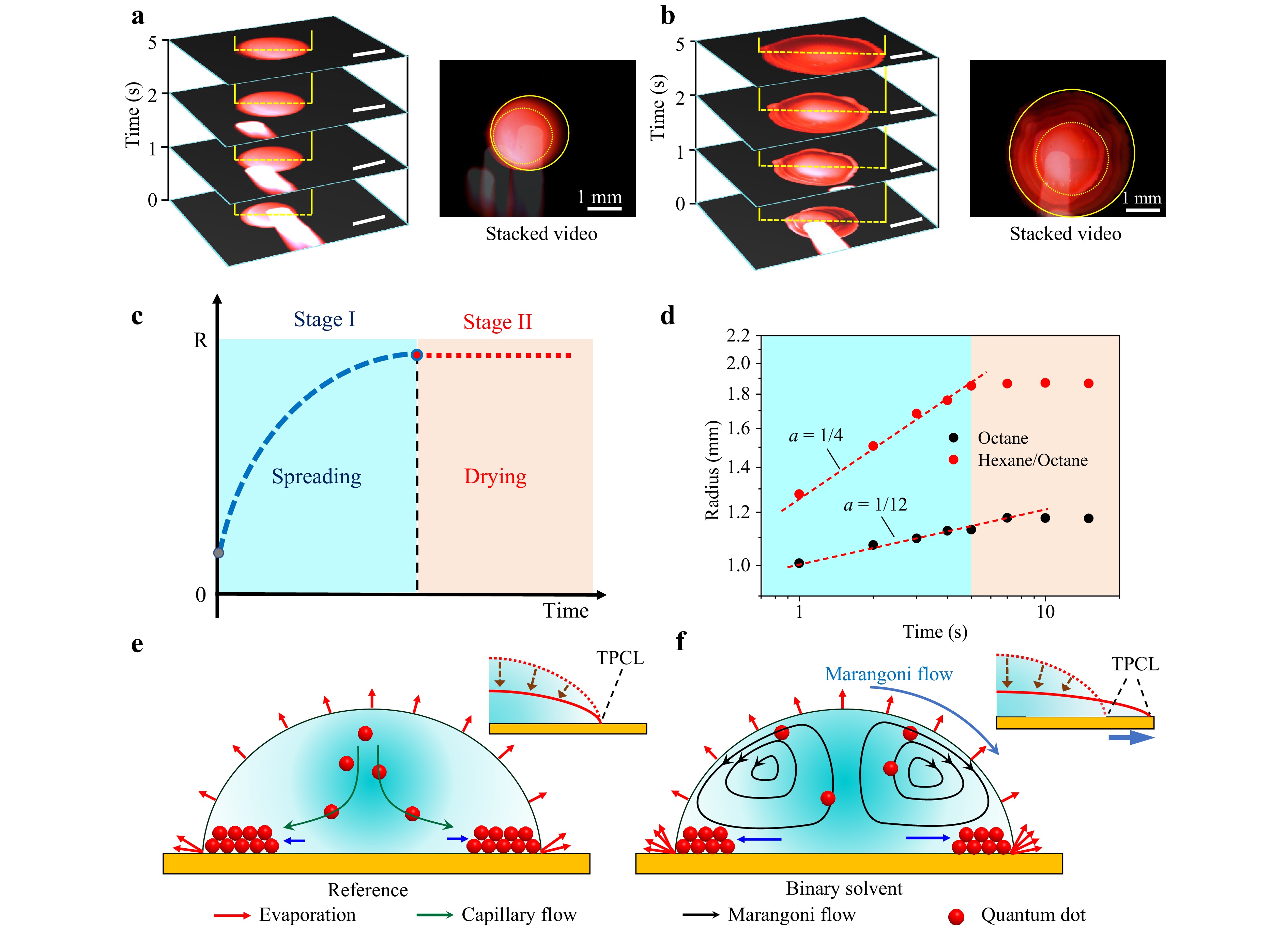
Fig. 2 In situ microscopic observations of the droplet spreading process. a Film formation process of QD inks in octane. The volume of a QD droplet is 0.2 μL. Stacked video frames from 0 s to 5 s show the spreading tracks of a QD droplet using octane solvent. The scale bars are 1 mm. b Film formation process of QD inks in binary solvents of hexane and octane. The volume of a QD droplet is 0.2 μL. Stacked video frames from 0 s to 5 s to show the spreading tracks of a QD droplet using a binary solvent of hexane and octane. The scale bars are 1 mm. c Schematic diagram of QD droplet spreading radius versus time in the film formation process. d The spreading radius-time (r-t) relationships in the droplet spreading stage using the octane and the binary solvent systems. Schematic diagrams of the solvent evaporation process, solvent flow, and three-phase contact line movement in the spreading process using e the octane system and f binary solvent of hexane and octane. The inset of e schematically shows the pinning effect of the three-phase contact line (TPCL) in the octane system. The inset of f schematically shows the mobile three-phase contact line of the binary solvent of hexane and octane.
To further explore the droplet spreading process, Fig. 2d shows the spreading radius-time (r-t) relationship during the droplet spreading stage. For the octane system, the spreading radius followed the relationship r ∝ t1/12, which could be considered a capillary-dominated spreading process (Fig. 2e)55,56. A minor capillary force can promote droplet spreading, but is unlikely to induce obvious motion of a three-phase contact line (Fig. 2e). For the binary solvent system, the spreading radius followed a steeper relationship: r ∝ t1/4, which was much higher than that of the octane system. This enhancement could be explained by the additional Marangoni flow owing to the vapour pressure difference between hexane and octane. The rapid evaporation of hexane at the three-phase contact line resulted in a higher proportion of octane. A surface tension gradient (∇γ) was formed, pointing inward (lower tension) from the periphery (higher tension)55,56. This was due to the higher surface tension of octane (21.1 mN·m−1) compared to that of hexane (18.1 mN·m−1), and led to the Marangoni flow (Fig. 2f). The generated Marangoni flow regulated the spreading dynamics and drove the outward migration of the three-phase contact line, thereby expanding the QD droplet spreading area in the binary solvents (Fig. 2f). All the solvent data were compiled from Yaws’ Handbook of Thermodynamic and Physical Properties of Chemical Compounds and Solvents (Fifth Edition).
We further investigated the effect of the hexane/octane volume ratio on the spreading area of the QD films. Fig. S1a shows photoluminescence (PL) images of the QD ink in octane and the binary solvent of hexane and octane. In comparison to octane, hexane has a lower boiling point (68.7 °C compared to 126 °C), as well as a smaller surface tension and lower viscosity (0.31 mPa·s compared to 0.54 mPa·s). Figs. S1b and 1c show the droplet spreading areas of the QD inks in the binary solvents of hexane and octane at a range of volume ratios. At a volume fraction of 30% hexane, the QD film coverage area was 42%, which was four times larger than that of the pristine octane system (8%). This phenomenon indicated an enhanced spreading area for the QD ink in the hexane/octane binary solvents with different volume ratios. Furthermore, the droplet-spreading behaviours of the QD inks on the Poly[(9,9-dioctylfluorenyl-2,7-diyl)-co-(4,4′-(N-(4-sec-butylphenyl)) diphenylamine)] (TFB) surface were investigated, with the results shown in Fig. S1d. The QD droplets exhibited an enhanced spreading area on the TFB surface, similar to that observed on a glass substrate.
To evaluate the influence of the mixed solvents on the film formation process, QD inks were prepared in a binary solvent of undecane and octane. In comparison to octane, undecane has a higher boiling point (196 °C), as well as a larger surface tension (24.8 mN/m) and higher viscosity (1.4 mPa·s). Figs. S2 and S3 show the droplet spreading areas of the QD inks in binary solvent of undecane and octane with different volume ratios. The pristine QD ink of octane typically spread at approximately 8%. At a volume fraction of < 40% for undecane, the droplet of the QD ink gradually spread with the coverage of 36%. When the volume ratio of undecane was > 50%, the droplets of QD ink gradually shrank with the coverage of 4%. In situ microscopy observations of QD ink (60% undecane) showed a smaller spreading area (3.9 mm2) compared to that of the octane system (4.3 mm2), indicating a decreased spreading area (Fig. S4). These results indicated that the use of QD inks in binary solvents enhances the ability to tune the droplet-spreading area.
We further evaluated the effect of the hexane/octane binary solvents on the morphology of the QD film and corresponding device efficiency. Fig. 3a, b show the scanning electron microscopy (SEM) images of the octane system and 30% hexane/octane system, respectively, showing uniform QD distributions without obvious cracks or agglomeration. In contrast, the 80% hexane system exhibited particle agglomeration (Fig. 3c). Fig. 3d-f and S5 show atomic force microscopy (AFM) images of the QD films with low surface roughness (Rq < 3 nm). The Rq of the 80% hexane system increased to 2.56 nm, indicating increased disorder of the QD particles.
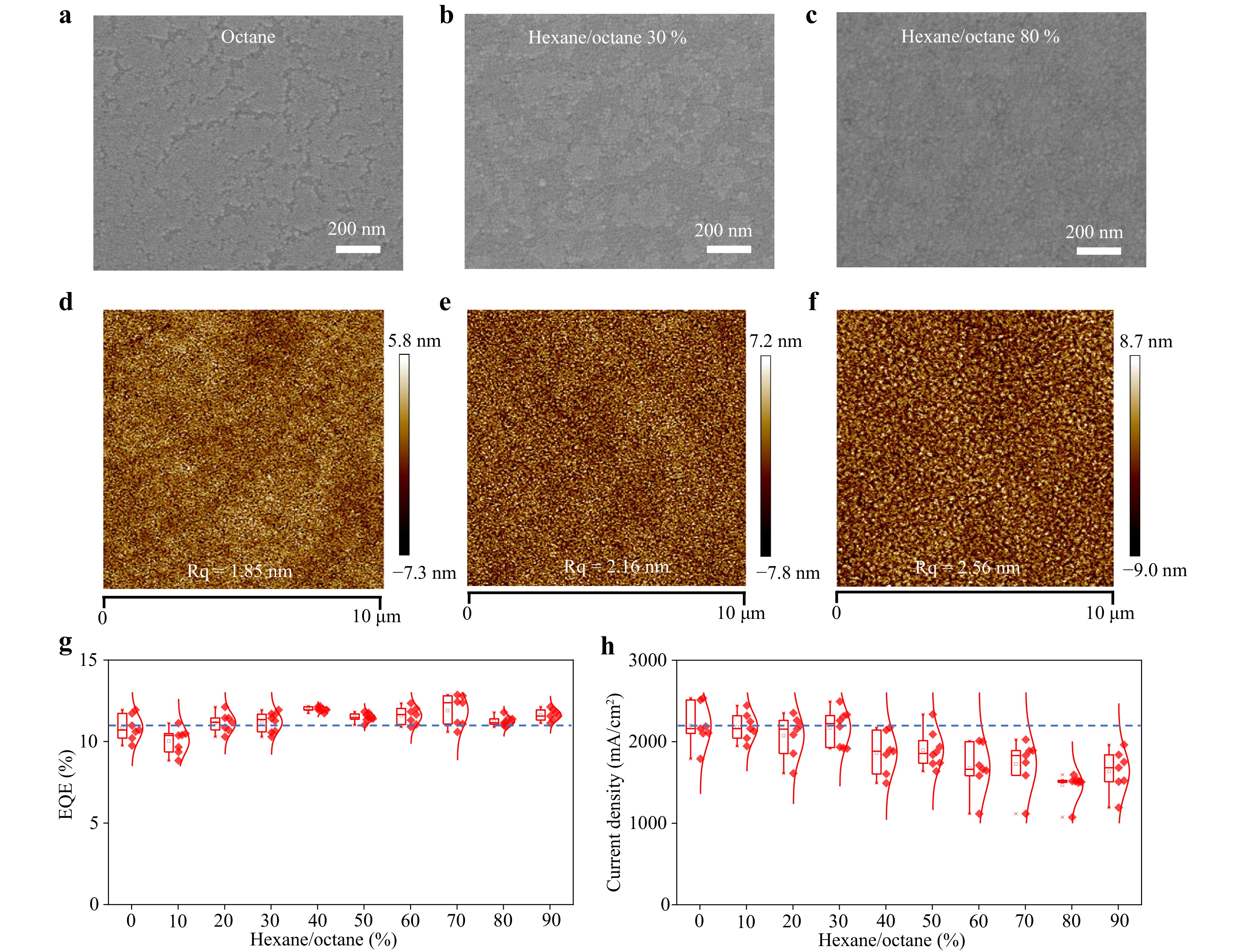
Fig. 3 Morphology of spin-coated QD layer. a-c SEM images of spin-coated QD films with hexane/octane volume ratios of 0, 30%, and 80%, respectively. Scale bars are 200 nm. d-f AFM images of spin-coated QD films with the hexane/octane volume ratios of 0, 30%, and 80%, respectively. g EQEs and h current densities of multiple QLED devices with a device architecture of ITO/PEDOT: PSS/TFB/QD/ZnMgO/Al using different hexane/octane volume ratios from 0 to 90%. The active area is 2 × 2 mm2. The data were collected from six samples. The error bars represent the standard deviation calculated from six independent measurements.
QLED devices were fabricated using QD inks with different hexane/octane ratios. The EQEs of the pristine and target devices were similar (Fig. 3g). The current density decreased significantly with an hexane solvent fraction of up to 50%, leading to a decrease in luminance (Fig. 3h and S6). Statistical data were collected for six samples under each condition. Error bars represent the standard deviations calculated from six independent measurements. We selected a QD ink with an hexane volume ratio of 30% for further wafer-scale fabrication. The QD solutions dispersed in octane and the 30% hexane/octane binary solvent showed similar morphologies, absorption values, and PL spectra, as well as a high photoluminescence quantum yield (PLQY) of 98%, indicating that the intrinsic QD properties were unchanged in the binary solvent (Figs. S7 and S8). We compared the operational lifetimes of red QLEDs fabricated with different QD solutions in octane and the binary solvents with 30% hexane (Fig. S9). The T95 lifetime is 4.99 and 6.24 h for octane (at an initial maximum luminance of 17,240 cd·m−2) and the binary solvent with 30% hexane (at an initial maximum luminance of 14,800 cd·m−2) respectively. Using an acceleration factor of n = 1.8 for lifetime conversion, the T95 lifetime at 1,000 cd·m−2 for the pristine device was calculated as 838 h. Similarly, the QLED fabricated by binary solvent with 30% hexane achieved a T95 lifetime at 1,000 cd·m−2 of 798 h, confirming the negligible impact on the QLED operational lifetime.
Fig. 4a, d, g, and Fig. S10 show the as-fabricated 2-inch wafer-scale Micro-QLED with a device architecture of ITO/PEDOT: PSS/TFB/QD/ZnMgO/Al. The 2-inch large-area QD film showed highly uniform PL emission and film thickness (Fig. S11). The pre-patterned substrates were fabricated using photolithography-template assisted processing31. Fig. S12 shows the contact angle of the photolithography template, which was to that of the pristine ITO substrate. All the functional layers of the QLED showed good wetting property. Fig. S13 shows the photolithography templates of different sizes, covering pixel sizes from 50 μm to 4 μm. Fig. 4b, c show the J-V-L and EQE curves of the 2-inch red-emitting Micro-QLED wafer, which achieved a peak EQE of 22.8%. For the 2-inch green-emitting Micro-QLED wafer, the device exhibited a peak EQE of 20.8% (Fig. 4e, f). For the 2-inch blue-emitting Micro-QLED wafer, the device exhibited a peak EQE of 1.4% (Fig. 4h, i). In addition, 2-inch pristine QLED devices were fabricated using ITO substrates with a uniform electroluminescence distribution (Fig. S14) and peak EQEs of 19.7% and 16.6% for the red and green devices, respectively (Fig. S15). The device architecture and fabrication process were the same for both the small-area (2 × 2 mm2) prototype QLEDs and large-area (40 × 40 mm2) wafer-scale QLEDs. However, the larger resistance of the ITO electrode on the large-area substrate led to a reduced current in the large-area QLED device.
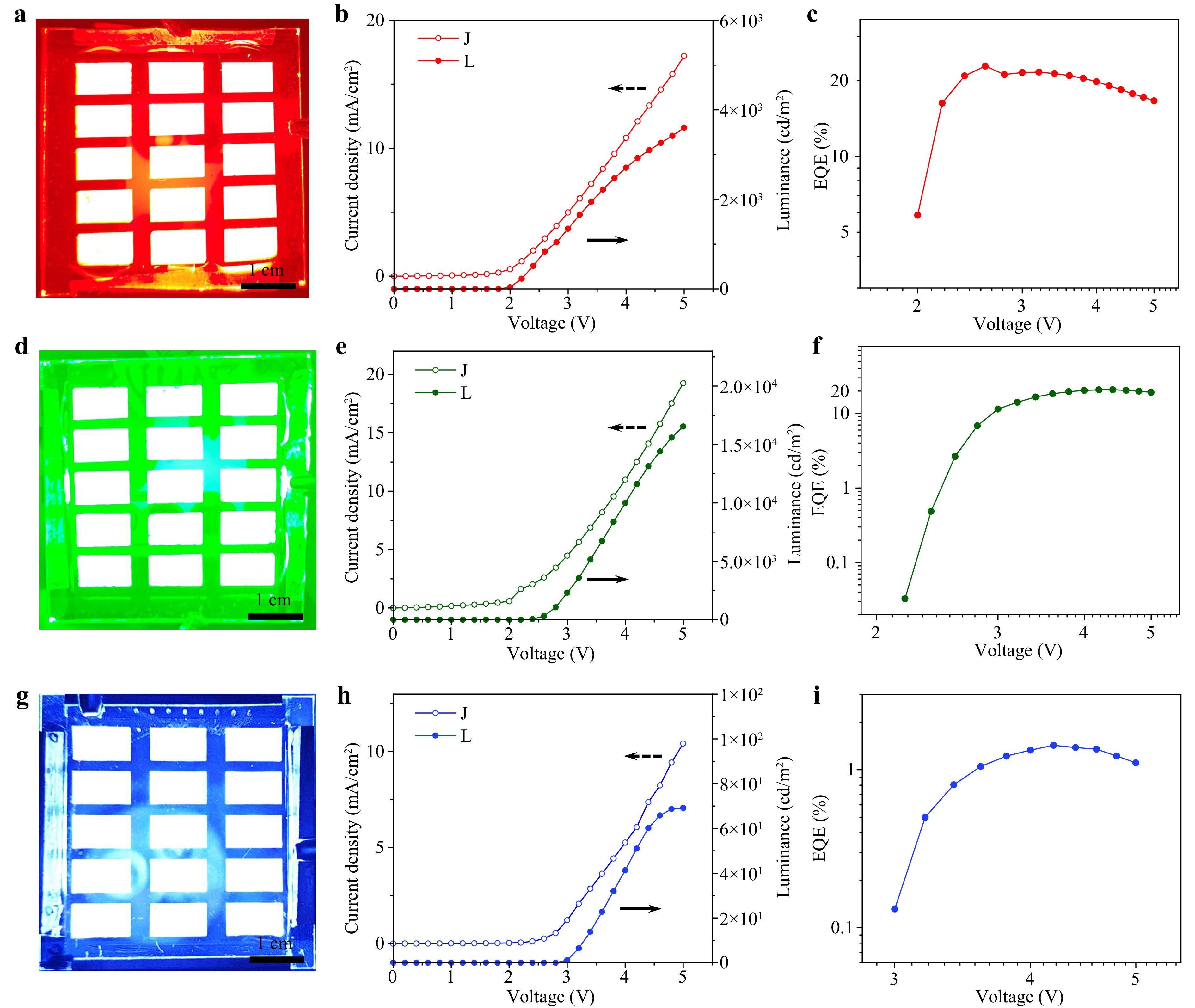
Fig. 4 Device performance of 2-inch Micro-QLEDs. a Electroluminescence images of a red-emitting Micro-QLED device (scale bar: 1 cm). b Current density–voltage–luminance (J–V–L) relationship and c EQE–voltage curves of 2-inch red-emitting Micro-QLED. d Electroluminescence images of green-emitting patterned Micro-QLED device (scale bar: 1 cm). e J–V–L and f EQE–voltage curves of 2-inch green-emitting Micro-QLED. g Electroluminescence images of blue-emitting patterned Micro-QLED device (scale bar: 1 cm). h J–V–L and i EQE–voltage curves of 2-inch green-emitting Micro-QLED.
Supplementary Table S1 summarizes the literature on large-area QLED and perovskite-based devices17,24-27,46-48,57-59. Solvent-engineering strategies have been explored for large-area PeLED fabrication, however the large-area device performance has rarely been evaluated. Supplementary Fig. S21 shows a performance comparison of the reported large-area QLEDs. The state-of-the-art 2-inch wafer-scale fabrication process for the Micro-QLED greatly improved the active emitting area and EQEs of the QLED devices.
The 2-inch Micro-QLED wafer could provide 15 Micro-QLED panels (0.46 inch each). (Fig. 5a). In the wafer-scale fabrication process, wafer dicing is a key step in achieving smaller chips while ensuring structural and functional integrity. Fig. S16 shows a schematic of the dicing process, in which a diamond knife was used to dice along these predefined gaps. The achieved 0.46-inch (0.56 cm × 1 cm) microdisplay chips showed uniform electroluminescence values (Fig. 5b, c, and S17). Fig. 5d-f show EL microscopy images, which verified that a resolution of 2,510 pixels per inch (ppi) was achieved (Figs. S18-S20). The Micro-QLED pixels emitted red, green, and blue light with a uniform distribution, demonstrating the feasibility of the 2-inch wafer-scale fabrication of RGB Micro-QLEDs.
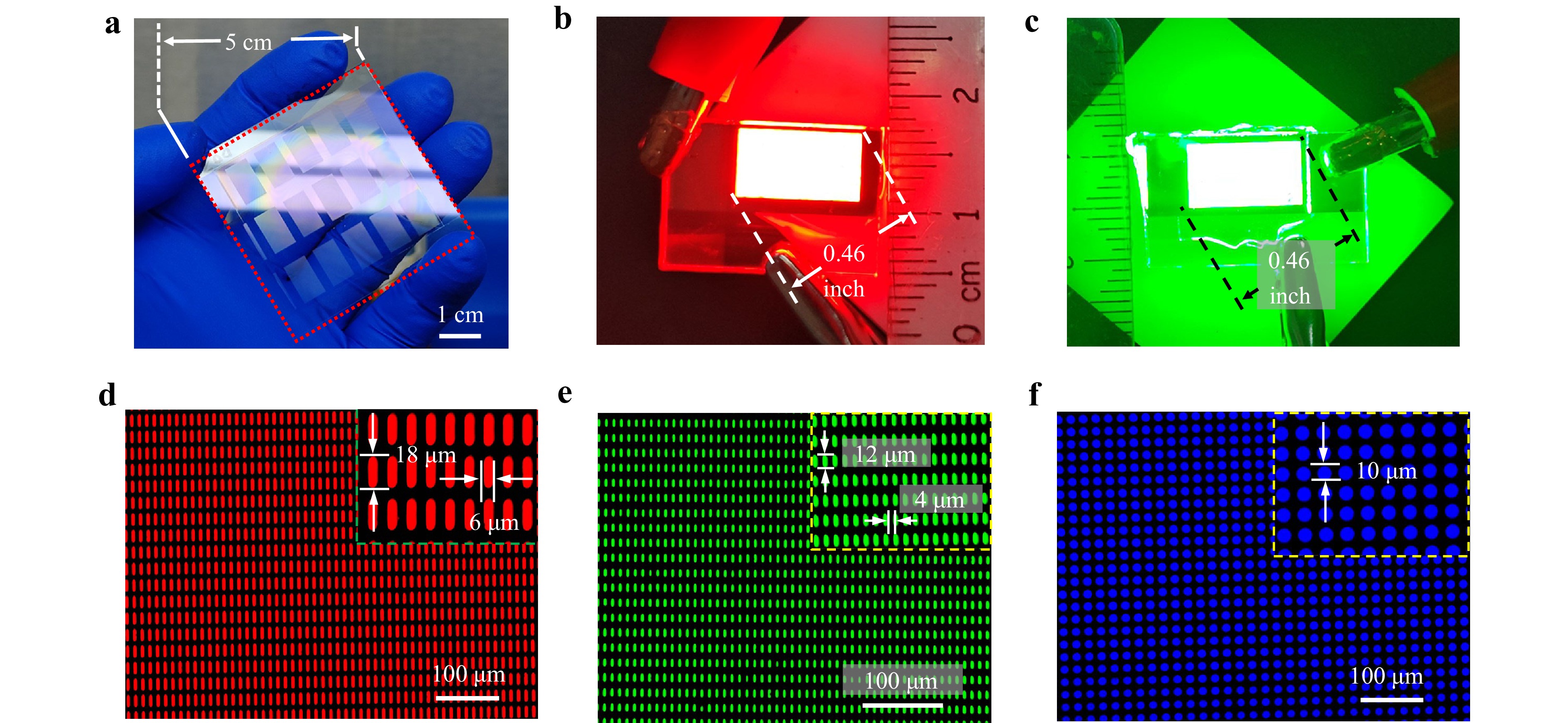
Fig. 5 Electroluminescence patterns of a 2-inch Micro-QLED. a Image of a 2-inch wafer-scale Micro-QLED. b, c Electroluminescence images of 0.46-inch Micro-QLED panels. d-f Electroluminescence optical microscopic patterns of red, green, and blue-emitting Micro-QLED devices.
This study demonstrated the feasibility of a 2-inch wafer-scale Micro-QLED fabrication strategy at the prototype level. Further scaling to larger wafers (4-inch and 8-inch), as well as an assessment of the compatibility with QLED industrial processes, still presents technical challenges. Large-area solution processing varies with the solvent evaporation, droplet spreading, and solution flow across the substrate. Therefore, the 8-inch wafer fabrication for micro-QLEDs requires further investigation.
-
In summary, we established a feasible manufacturing strategy for 2-inch Micro-QLED wafers by combining solvent engineering and photolithography-template assisted processing. The 2-inch wafer could provide 15 microdisplay panels of 0.46-inch with a resolution of 2,510 ppi (pixel size from 4 to 50 μm), achieving peak EQEs of 22.8%, 20.8%, and 1.4% for the red, green, and blue Micro-QLEDs, respectively. Using QD inks in a binary solvent of hexane/octane made it possible to control the droplet spreading and fabricate 2-inch wafer-scale Micro-QLED devices via spin coating. Because hexane has a lower boiling point and surface tension than octane, the mixed solvent could effectively tune the evaporation behaviour and drying dynamics during spin coating. Based on in situ microscopic observations, we illustrated the solvent evaporation-induced surface tension gradient and subsequent Marangoni flow during droplet spreading. To achieve wafer-scale fabrication, the spreading of the QD droplets can be controlled by introducing a Marangoni flow. These will significantly advance the industrialization of Micro-QLED for AR microdisplay applications.
-
Lithium hydroxide, magnesium acetate tetrahydrate, ethanol, DMSO, and zinc acetate dihydrate were obtained from Shanghai Aladdin Technology Co., Ltd. The polymer TFB and PEDOT:PSS 4083 solutions were sourced from Xi'an Polymer Light Co., Ltd. QD solutions (red and green CdSe/ZnS QDs and blue CdZnSe/ZnS QDs) were obtained from TCL, Inc. Oleic acid, oleylamine, and 1-octanethiol were used as surface ligands, the photoresist (EOC-260) was obtained from the Hefei Innovation Research Institute of Beihang University.
-
A 0.2 μL QD droplet was deposited onto a glass substrate using a micropipette. The droplet spreading process was observed in real time using an optical microscope (Olympus, BX3M) and recorded using a high-speed camera (SSZN, Eco 3-105-M-32). The microscope was operated at 5× magnification and coupled with a high-speed camera capable of 240 fps with a time resolution of approximately 4.17 ms. Spreading area data were calculated using ImageJ software. Finally, the spreading area and spreading radius–time (r–t) relationships in the droplet spreading stage were obtained.
-
ZnMgO nanoparticles were synthesised by the dropwise addition (0.5 mL/min) of a LiOH/ethanol solution into a 15 mL DMSO solution containing Zn(OAc)2·2H2O (1.35 mmol) and Mg(OAc)2·4H2O (0.15 mmol) under a nitrogen atmosphere. The precursor solution was prepared by dissolving 2.5 mmol LiOH in ethanol (25 mL), followed by sonication at 40 kHz/300 W for 20 min. The mixture was subsequently heated at 50 °C for 2 h to form ZnMgO nanoparticles. The nanoparticles were then washed twice with an ethanol/ethyl acetate mixture via centrifugation, and finally redispersed in ethanol at 20 mg·mL−1.
-
A micrometre-scale template was produced using an EOC-260 photoresist through a series of lithographic steps. First, the glass substrates underwent a sequential ultrasonic cleaning process in deionised water, ethanol, and acetone for 15 min each, followed by oxygen plasma treatment at 100 W for 5 min. The photoresist film was then applied via spin coating at 7,000 rpm for 1 min, and baked at 80 °C for 5 min on a heating plate. The micrometre-scale pattern was defined using UV lithography at an exposure dose of 50–100 mJ·cm−2. After UV exposure, the unexposed photoresist was removed by developing the substrates in the PGMEA solvent, assisted by 60 s of sonication. Finally, to enhance the structural stability of the template, hard baking was performed at 230 °C for 30 min.
-
The fabrication of the 2-inch Micro-QLED wafer followed the device architecture of ITO/PEDOT:PSS/TFB/QDs/ZnMgO/Al. First, following the oxygen plasma treatment of the pre-fabricated templates, a PEDOT:PSS hole-injection film was applied via spin-coating (3,000 rpm, 45 s) and subsequently heated at 150 °C for 30 min in air. The subsequent steps were performed in a N2 glovebox, ensuring an oxygen and moisture content below 1 ppm. A TFB hole-transport layer was applied by spin-coating a 6 mg·mL−1 chlorobenzene solution at 2,000 rpm for 30 s, forming a uniform film. This was followed by a thermal annealing step at 150 °C for 30 min. The emissive QD layer was applied using a 20 mg mL−1 octane solution via spin-coating (2,000 rpm, 30 s), followed by an annealing process (80 °C, 10 min). Subsequently, the ZnMgO layer was formed by spin-coating an ethanol-based ZnMgO nanoparticle solution under the same spin conditions (2,000 rpm, 30 s), and cured (90 °C, 30 min). The final step was the thermal evaporation of the aluminium electrode using a Kurt J. Lesker Mini Spectros system. The control devices were fabricated using ITO substrates.
-
The morphologies of the devices were characterised using SEM (Hitachi Regulus 8230) and AFM (Bruker Dimension Fast Scan). The electroluminescent performance of the large-area (5 × 5 cm) and small-area (2.5 × 2.5 cm) QLEDs were evaluated with a Zolix PR788 system and custom optoelectronic measurement station, respectively. The custom station was equipped with key components, including an Avantes HSC-TEC spectrometer, a Thorlabs FDS1010 photodetector, an integrating sphere, and a Keithley 2400 source. An optical microscope was used to obtain the Micro-QLED images.
-
This study was supported by the National Natural Science Foundation of China (grant number: U23A20683) and Beijing Municipal Science & Technology Commission, Administrative Commission of Zhongguancun Science under Park No. Z231100006023018 and the National Natural Science Foundation of China (grant number: 12272390).
Two-inch wafer-scale manufacturing of Micro-QLED for AR microdisplay application
- Light: Advanced Manufacturing , Article number: 91 (2026)
- Received: 28 January 2026
- Revised: 01 May 2026
- Accepted: 06 May 2026 Published online: 02 June 2026
doi: https://doi.org/10.37188/lam.2026.091
Abstract: Micrometre-sized quantum-dot light-emitting diodes (Micro-QLEDs) have been successfully demonstrated as a promising technology for augmented reality (AR) microdisplay applications. To facilitate industrial applications, we developed a two-inch wafer-scale fabrication process for Micro-QLEDs, including the fabrication of a photolithography template, spin-coating fabrication of a QLED, and dicing of a 2-inch wafer into 0.46-inch Micro-QLED panels. Considering the challenge posed by the limited droplet spreading of quantum dots during spin-coating fabrication, we introduced a binary solvent of hexane and octane to achieve a wafer-scale spreading area. In situ high-speed microscopic observations revealed the critical role of Marangoni flow in determining the dynamics of a three-phase contact line. We further designed a 2-inch wafer-scale fabrication process for Micro-QLEDs with an active emitting area of 1,600 mm2, which provides fifteen microdisplay panels with a 0.46-inch Micro-QLED per wafer, achieving a resolution of 2,510 pixels per inch (a pixel size range of 4–50 μm). In addition, the red, green, and blue Micro-QLED wafers had high external quantum efficiencies of 22.8%, 20.8%, and 1.4%, respectively. The 2-inch wafer-scale fabrication process for Micro-QLEDs provides a feasible method for the industrialisation of Micro-QLED technology.
Research Summary
AR display: Wafer-scale fabrication of Micro-QLED panels
Microdisplay panels are a key component of AR glasses. Quantum-dot light-emitting diodes (QLEDs) show advantages such as high brightness, high resolution, and easy fabrication, making them a promising approach for microdisplay panels. High-resolution Micro-QLEDs have been successfully demonstrated through a photolithographic patterning process. Recently, Haizheng Zhong from Beijing Institute of Technology and Weibin Li from the Chinese Academy of Sciences reported 2-inch wafer-scale manufacturing of high-resolution Micro-QLEDs using photolithography template-assisted processing. They fabricated 15 0.46-inch Micro-QLED panels on a 2-inch wafer with a resolution of 2510 pixels per inch. This is a milestone in the progress of Micro-QLED toward AR applications.
Rights and permissions
Open Access This article is licensed under a Creative Commons Attribution 4.0 International License, which permits use, sharing, adaptation, distribution and reproduction in any medium or format, as long as you give appropriate credit to the original author(s) and the source, provide a link to the Creative Commons license, and indicate if changes were made. The images or other third party material in this article are included in the article′s Creative Commons license, unless indicated otherwise in a credit line to the material. If material is not included in the article′s Creative Commons license and your intended use is not permitted by statutory regulation or exceeds the permitted use, you will need to obtain permission directly from the copyright holder. To view a copy of this license, visit http://creativecommons.org/licenses/by/4.0/.

 DownLoad: