






-
Terahertz (THz) is an electromagnetic wave with a frequency of 0.1~10 THz, a region historically referred to as “terahertz gap” in the electromagnetic spectrum. THz waves offer attractive properties including strong penetration, large bandwidth, high speed, and biological safety; however, naturally occurring materials capable of effective THz control remain scarce. The emergence of metasurfaces1 provides a promising solution to this challenge. Metasurfaces can be regarded as a branch of metamaterial technology that enables artificial manipulation of incident electromagnetic waves through two-dimensional arrays of subwavelength resonant structures. They can achieve magical functions such as wave absorption2–4, focusing5, phase modulation6, and polarisation conversion7.
Carbon-based materials possess unique electrical, optical, thermal, and mechanical properties, making them ideal candidates for next-generation flexible optoelectronic devices8. These materials primarily include carbon black (CB)9, carbon nanotubes (CNTs)10, graphene11, and their derivatives such as graphene oxide (GO)12, which have potential applications in semiconductors, flexible circuits, sensors, and other fields13–15. By combining carbon-based nanomaterials with metasurfaces, we can make full use of their advantages to realise the innovation of both materials and structures to comprehensively surpass devices made of natural materials and lay the foundation for the next-generation flexible optoelectronic devices.
However, the unit size of a THz metasurface is in the subwavelength scale, which imposes strict requirements on the manufacturing process. Traditional techniques, such as photolithography, coating, and etching, can meet precision requirements but are limited by time constraints, complex processes, and high costs. By contrast, 3D direct-write printing in additive manufacturing technology offers a low-cost and low-complexity fabrication solution. This enables patterning on rigid substrates (e.g. silicon wafers and glass) and flexible materials (e.g. PET, PI, and paper)16–20, providing high compatibility with both substrates and inks. This flexibility makes it highly promising for THz flexible metasurface fabrication, and considerable research has validated the application potential of this technology in the field21–23. Inkjet printing is the basic mode of 3D direct-write printing. By applying pressure to the ink, a jet with a diameter comparable to the inner diameter of the nozzle was formed, enabling patterning on the substrate. This mode is simple and fast; however, the printing resolution is often limited by the inner diameter of the nozzle. Electrohydrodynamic jet (E-jet) printing can be adopted to achieve higher precision. E-jet printing24 is a microdroplet spray-deposition moulding technology based on electrohydrodynamic principles. It uses an electric field between the nozzle and substrate to drive and “pull” the ink, generating a Taylor cone at the nozzle tip that is significantly smaller than the nozzle diameter25, enabling the printing of higher resolution structure lines.
In this study, we propose a simple and highly efficient carbon-based additive manufacturing approach for flexible THz metasurfaces by combining inkjet and E-jet printing with carbon-based nanomaterial inks. This not only enables the preparation of complex resonant structures using direct-write printing, but also allows the use of different inks to adjust the characteristics of the cell structure, thereby facilitating a more flexible design of THz metasurfaces. Herein, we present the preparation methods and properties of three different carbon-based inks: carbon black-based (CB), graphene-based, and GO-based (graphene oxide-based). Moreover, we designed two metasurface THz absorbers and a filter operating in different frequency bands. The resonant structures were printed using graphene-based, GO-based, and CB-based inks. They offer great flexibility in choosing substrate materials such as paper and polyethylene terephthalate (PET). As a common flexible material, paper is eco-friendly and low-cost, whereas PET is resistant to moisture and corrosion and highly transparent. Next, two printing modes were used (inkjet printing and E-jet printing) to prepare the metasurfaces. The inkjet mode is simple, fast, and does not require the application of a high-voltage electric field to protect the material properties, whereas the E-jet printing mode requires the application of a high-voltage electric field, which has higher accuracy and can be used for materials that can resist high voltages. The fabrication scheme enables high-efficiency dual-mode additive manufacturing, while offering flexibility in the substrate choice and resonance-pattern design.
-
Fig. 1 shows a carbon-based additive manufacturing method for flexible THz metasurfaces. The main process is shown in Fig. 1a and includes the following steps: (1) preparation of the carbon-based ink, (2) property testing, (3) simulation and optimisation of the metasurfaces, and (4) direct write printing. In the first step, various carbon-based inks are prepared using different carbon nanomaterials (such as carbon black, graphene, and graphene oxide), as shown in Fig. 1b. Among them, carbon black not only exhibits low resistivity, but is also cost-effective and easy to obtain, making it an excellent conductive material. Graphene, renowned for its ultrahigh electrical and thermal conductivities, is widely used in flexible and tunable devices. Graphene oxide, a derivative of graphene, can be reduced to reduced graphene oxide (rGO) under electrical or thermal stimulation, achieving an increase in electrical conductivity of one to three orders of magnitude26. This property makes graphene oxide suitable for preparing tunable metasurfaces. Then, the carbon-based inks were obtained by mixing the raw material, diluent, and binder, and then loaded into a syringe, as shown in Fig. 1c, d. Next, a dual-mode printing system, illustrated in Fig. 1e, was employed for direct writing of the metasurfaces. As shown in Fig. 1f, the printing head achieved high-precision printing by forming a jet at the nozzle tip. Fig. 1g, h show examples of THz metasurface devices printed using this method.
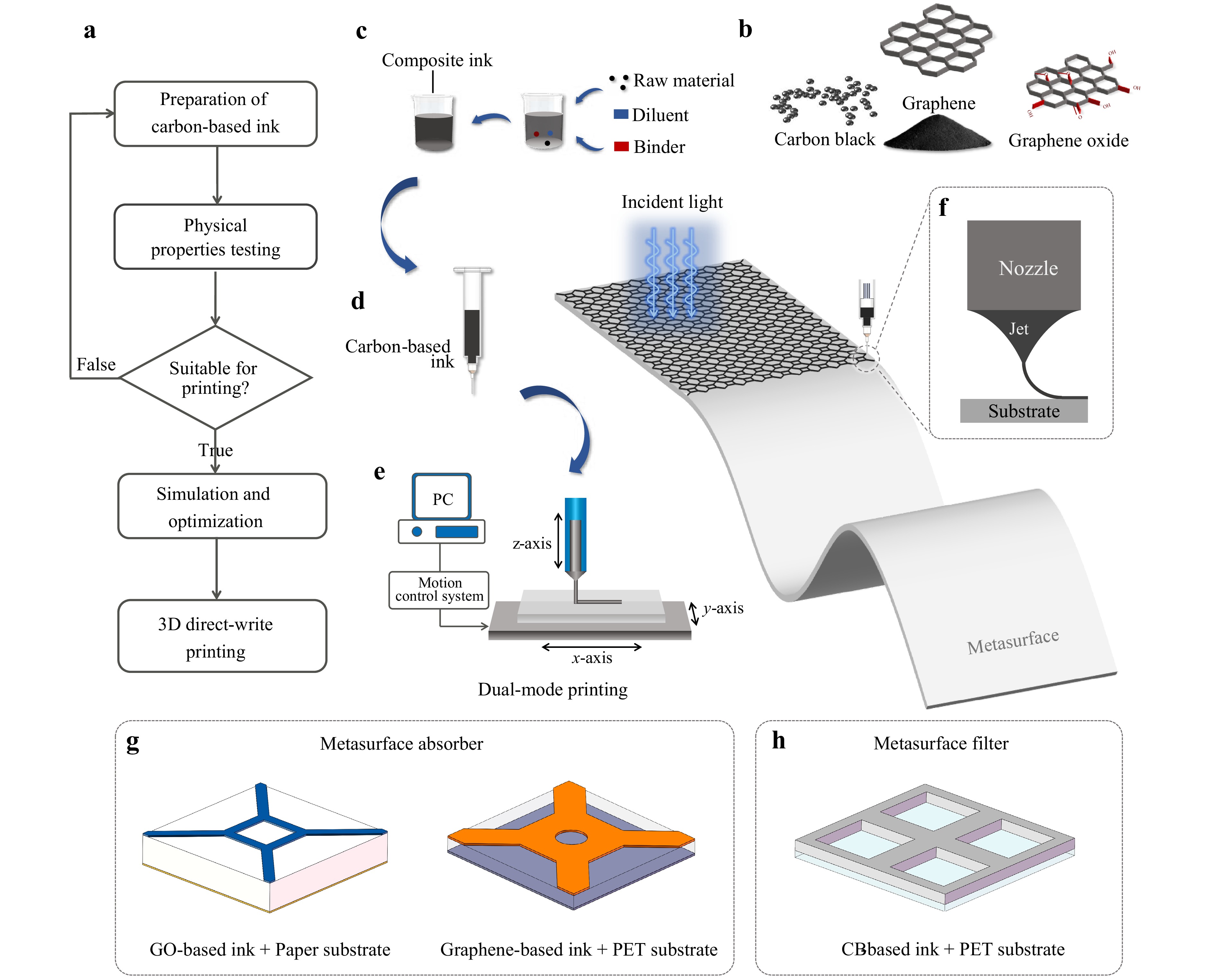
Fig. 1 a Flowchart of the carbon-based additive manufacturing method. b Carbon-based materials: carbon black, graphene, graphene oxide. c Carbon-based ink preparation process. d Schematic of syringe. e Schematic of dual-mode printing system. f Schematic of 3D direct-write printing. g Structures of the metasurface absorbers. h Structure of the metasurface filter.
To explore the effect of the doping ratio on the resistivity of the carbon-based metamaterials, samples were prepared by controlling the concentration of the carbon-based materials, and the electrical properties of each group of samples were tested. Fig. 2a illustrates the preparation of the carbon-based ink. Fig. 2b-d show the block-shaped specimens (30 mm × 8 mm × 0.01 mm). Fig. 2e-g show the sheet resistances of the samples with varying weight percentages of carbon nanomaterial powders. (See details in S1: Preparation of carbon-based ink). As can be seen from Fig. 2e, the sheet resistance decreases with increasing carbon black content, from approximately 40 Ω·sq−1 at 18% to 12.75 Ω·sq−1 at 35%. Fig. 2f illustrates a decrease in sheet resistance with the addition of graphene, dropping from 362.1 Ω·sq−1 at 1% to 47.35 Ω·sq−1 at 5%. It should be noted that graphene oxide differs from carbon black and graphene that it exhibits insulating properties at room temperature. To adjust the initial sheet resistance of the GO-based ink, carbon black powder was added to the formulation. Consequently, the sheet resistance of the GO-based ink increases with the weight percentage of graphene oxide, as shown in Fig. 2g. The prepared ink was loaded into a syringe and matched with a flat-bladed stainless-steel needle for subsequent printing.
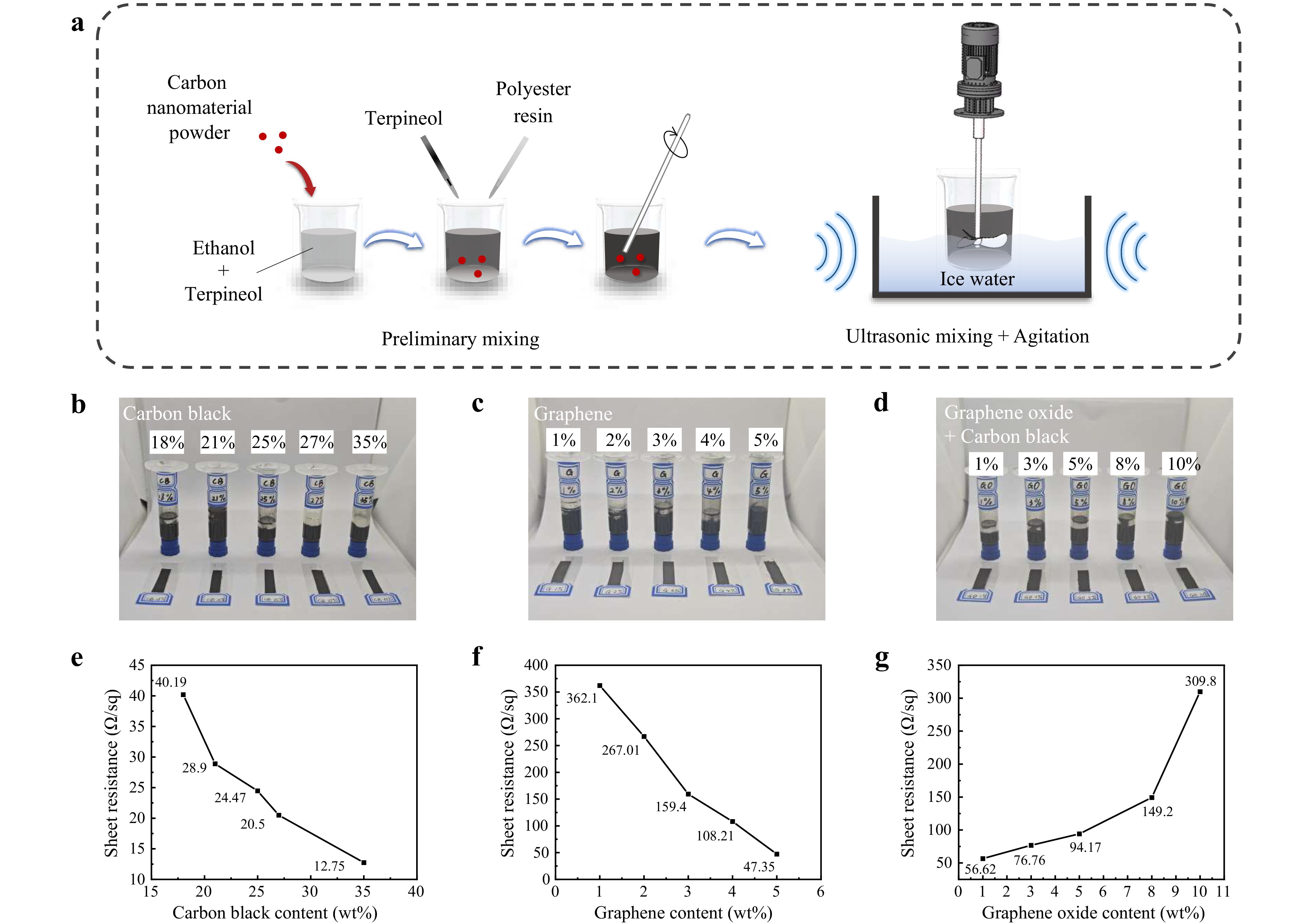
Fig. 2 a Preparation process of carbon-based ink. b Photograph of CB-based ink. c Photograph of graphene-based ink. d Photograph of GO-based ink. Sheet resistances for different weight percentages of carbon-based powder in inks: e CB-based ink; f Graphene-based ink; g GO-based ink.
-
The carbon-based additive manufacturing system included two printing modes: inkjet and E-jet printing. The inkjet mode is illustrated in Fig. 3a. Driven by a motor, a jet is formed and deposited on a substrate without applying an electric field. The E-jet mode is shown in Fig. 3b. With a high-voltage electric field, it can produce a smaller conical jet, and thus achieve higher precision. Fig. 3c shows the system, which mainly consists of a three-axis displacement platform, a dual-mode printing head, a print platform, and a high-voltage power supply. The printing head was responsible for discharging and forming high-precision printing lines. The three-axis displacement platform controls the printing head to realise the direct writing printing of the metasurface resonance pattern. A high-voltage power supply was used to generate the Taylor cone in E-jet mode. The dual-mode printing head is a critical component of the printing system and comprises a high-precision stepper motor, screw, storage syringe, and support frame. By controlling the rotational speed of the stepper motor, the upward and downward moving speeds of the slider could be controlled to achieve high-precision control of the injection feeding speed during printing. According to the motion parameters of the stepper motor, the minimum moving speed of the plunger is about 0.248 μm·s−1. Moreover, the system allows printing head switching during the process. The detailed steps are provided in Supplementary Document S2.
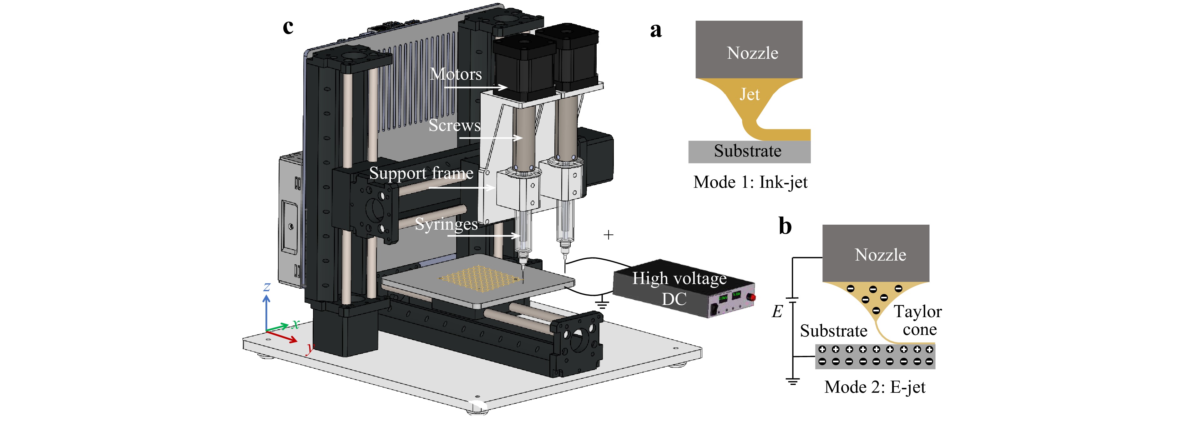
Fig. 3 a Schematic of inkjet printing. b Schematic of E-jet printing. c Schematic of the 3D printing system.
When using the inkjet mode, the motor squeezes the ink inside the syringe and deposits it onto the substrate, forming a patterned structure according to the path planning of the G-code slicing file. Inkjets are the basic mode of carbon-based printing. In this mode, the main determinants of the linewidth are the inner diameter of the nozzle, feeding rate, and nozzle moving speed. As shown in Fig. 4a, we focused on three adjustable printing parameters. The variable control method was adopted to analyse one printing parameter while keeping the other process parameters unchanged. When adjusting the nozzle size, the feed speed is fixed at 0.992 μm·s−1 and the printing speed is set at 20 mm·s−1. Fig. 4b illustrates the influence of the nozzle size on the printed line width, revealing a direct proportionality between the line width and the inner diameter of the nozzle. When changing the feeding rate, the nozzle size to 0.21 mm and the printing speed was set to 20 mm·s−1. Fig. 4c shows the effects of different feeding rates on the printed line width, indicating that the line width is directly proportional to the feeding rate. When adjusting the printing speed, set the nozzle size to 0.21 mm and the feeding rate to 0.992 μm·s−1. Fig. 4d demonstrates that the linewidth decreases as the moving speed increases, reflecting an inverse proportionality. The results of inkjet printing under different conditions and printed lines are shown in Fig. 4e.
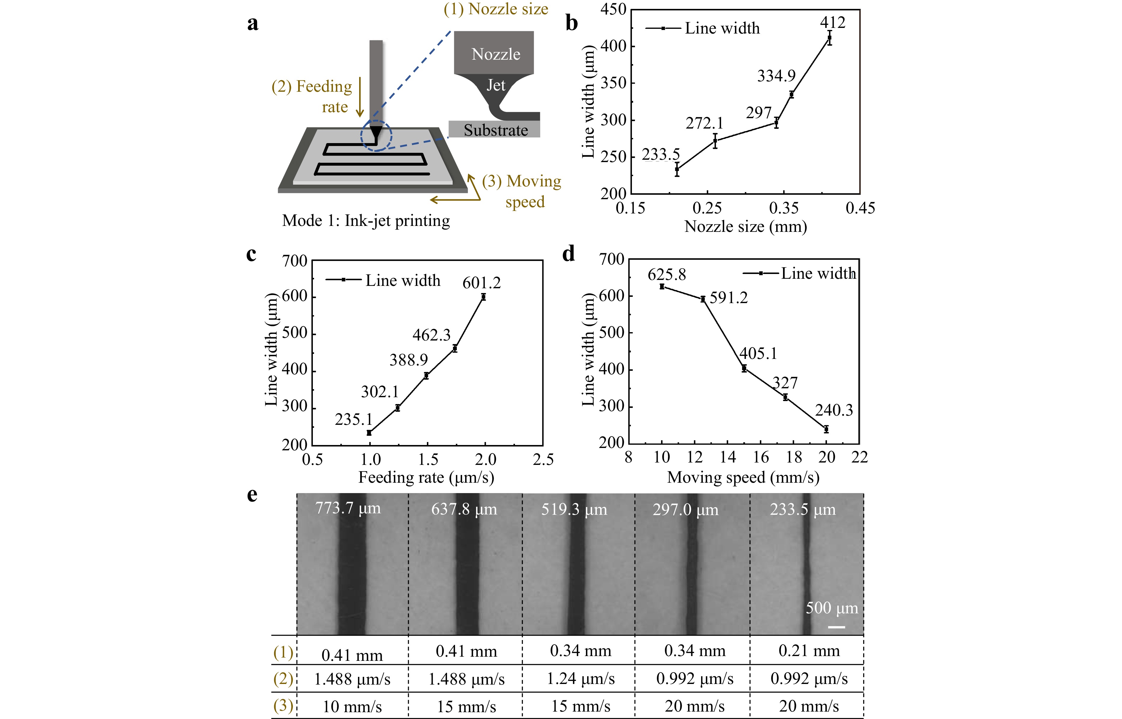
Fig. 4 a Schematic of inkjet mode and printing parameters. b Printed line width relation to the nozzle size (inner diameter). c Printed line width relation to the feeding rate. d Printed line width relation to the nozzle moving speed. e Five printing effects under different printing parameters.
When using the E-jet mode, a high-voltage power supply that can provide a voltage of 0–30 kV should be added. The positive terminal of the power supply was directly connected to the stainless-steel nozzle, whereas the printing platform was grounded. This setup established an electric field between the nozzle and substrate, energising the droplets at the nozzle to generate induced charges and become a Taylor cone27. By gradually increasing the voltage, the forces at the tip of the Taylor cone became unbalanced and formed a conical jet. According to Gañán-Calvo et al.28, the diameter of the jet diameter is directly proportional to the fluid flow rate. Therefore, the diameter of the jet was proportional to the feeding rate and inversely proportional to the nozzle speed. According to the proportionality proposed by Choi et al.29, the diameter of the conical jet, d, can be expressed as
$$ d\propto \sqrt{\frac{\gamma }{{\varepsilon }_{0}}}\frac{\sqrt{{d}_{\rm N}}}{E} $$ (1) where γ is the surface tension of air-ink interface, ε0 is the permittivity of free space, dN is the diameter of the nozzle, and E is the electric field strength.
Accordingly, conical jets of different sizes can be obtained by optimising the printing parameters such as the applied voltage, feeding rate, ink properties, needle size, and moving speed. In this study, we focused on three key printing parameters: the feeding rate, applied voltage, and nozzle moving speed, as shown in Fig. 5a. Because the printing distance directly affects the electric field force on the Taylor cone liquid surface, the distance between the tip nozzle and grounding substrate was fixed at 0.3 mm. A 27G stainless-steel nozzle (nozzle length: 13 mm, inner diameter: 0.21 mm) was applied to the printing head of the system. The effects of E-jet printing were tested under different conditions, and the printed lines were characterised. Fig. 5b illustrates the influence of the feeding rate on the printed line width, revealing a direct proportionality between the linewidth and feeding rate. Fig. 5c shows the effects of different voltages on the printed line width, indicating that the line width decreased as the voltage increased, reflecting inverse proportionality. Fig. 5d shows that the linewidth was inversely proportional to the moving speed. The five results of E-jet printing under different conditions and printed lines are shown in Fig. 5e. The minimum characteristic line width is 55.1 μm under the conditions of 2.8 kV voltage and 20 mm·s−1 moving speed and 0.248 μm·s−1 feeding rate.
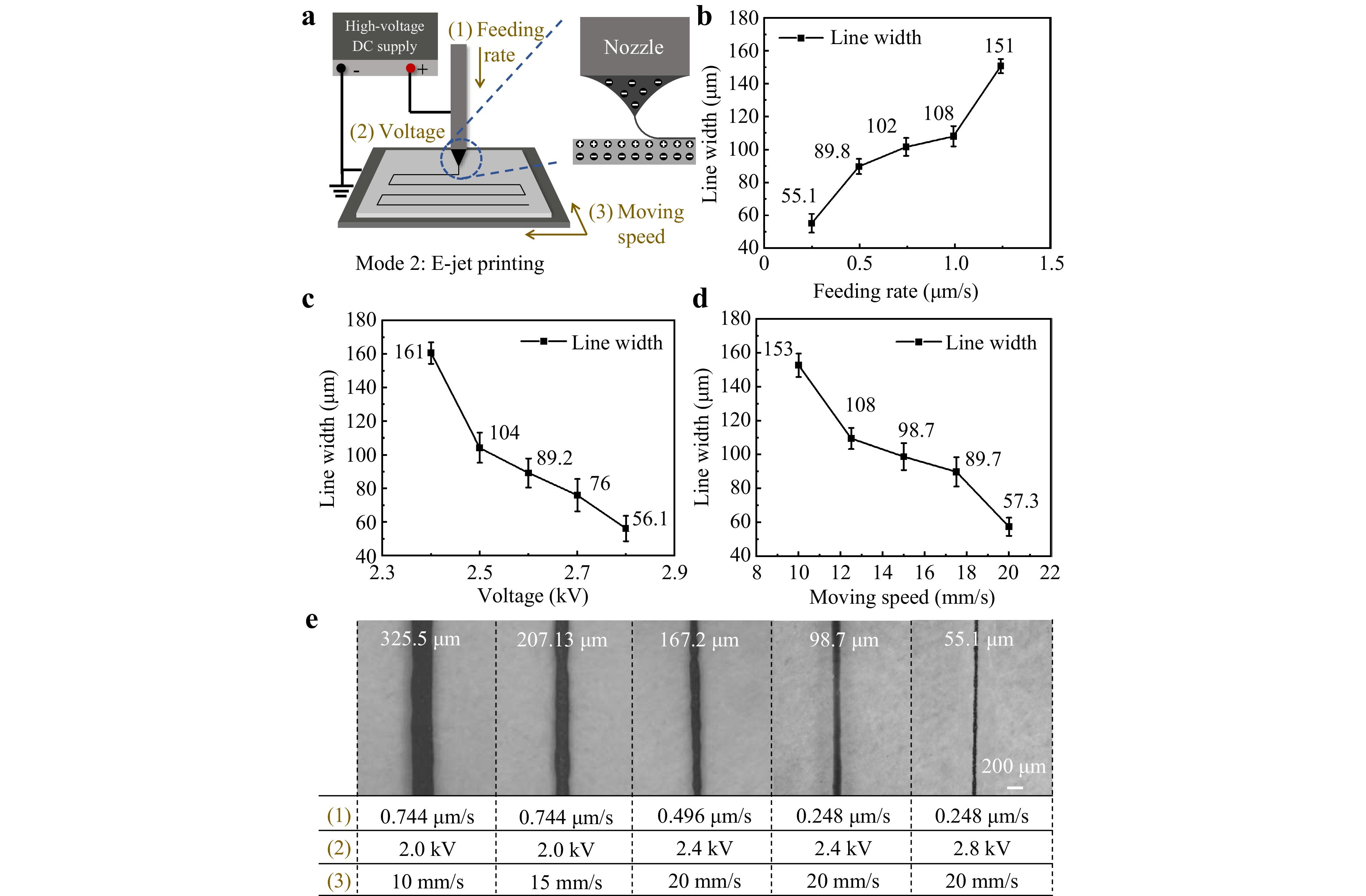
Fig. 5 a Schematic of E-jet mode and printing parameters. b Printed line width relation to the feeding rate. c Printed line width relation to the applied voltage. d Printed line width relation to the nozzle moving speed. e Five printing effects under different printing parameters.
The viscosities of the inks with different formulations also varied. Therefore, before printing metasurface structures, it is necessary to conduct printing parameter studies for each ink type. The detailed method for determining the printing parameters is provided in Supplementary document S3.
-
To validate the feasibility of this method, two carbon-based flexible THz-metasurface absorbers and a THz-metasurface filter were designed, simulated, and fabricated. To verify the flexibility of the substrates, two flexible substrates (paper and PET) were selected. Among them, the paper-based metasurface absorber has smaller unit structure, corresponding to the high frequency band (1.09~1.23 THz); the PET-substrate metasurface absorber has larger unit structure, corresponding to the low frequency band (0.30~0.38 THz); the metasurface filter based on PET substrate works near 0.8 THz.
The structure of a paper-based metasurface absorber is shown in Fig. 6a. It comprises three layers: a resonant structural layer, dielectric layer, and ground layer. The top layer serves as a resonant structure composed of a carbon-based ink that enables electromagnetic wave absorption. The specific structural parameters are shown in Fig. 6b. The second layer consisted of paper that functioned as the dielectric layer. The third layer was a conductive copper layer, which acted as the ground layer for the metasurface absorber. In the following section, we describe how absorption is achieved in detail. The commercial electromagnetic simulation software CST 2016 was used for this simulation. In the simulation process, the boundary conditions were set to the unit cell in the x and y directions and open (add space) in the z direction based on the Floquet mode. A tetrahedral meshing and frequency-domain solver based on the finite element method were used for the simulation. The background material is set to air and its dielectric constant is set to 1; the sheet resistance of the structural layer material is set to 50 Ω·sq−1; the dielectric constant of paper is set to 2.31.
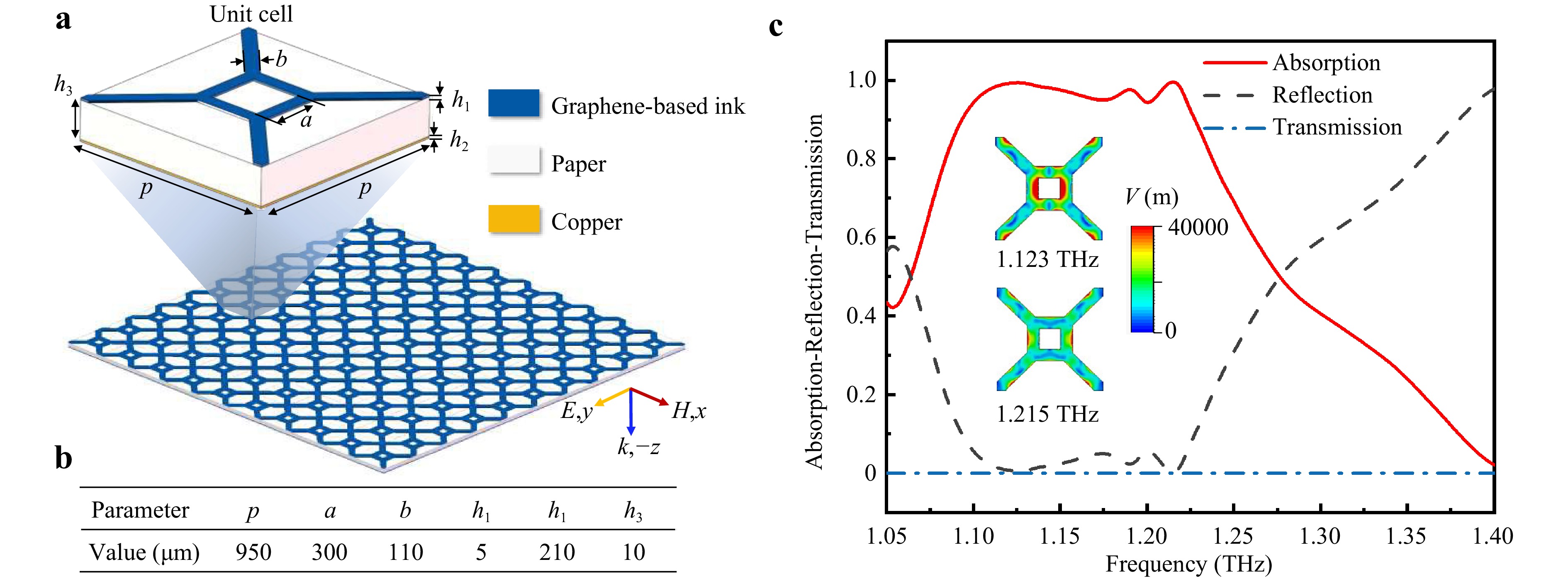
Fig. 6 a Schematic of the periodic cell array and the key dimensional parameters of the unit cell structure. b Size diagram of the paper-based metasurface absorber unit. c Simulated result of the paper-based metasurface absorber.
Considering that the size of the metasurface unit is much smaller than the wavelength, it can be regarded as an equivalent medium with complex dielectric constant ε and complex permeability µ. When the metal resonant layer strongly couples with the electric and magnetic fields, the equivalent impedance of the whole metasurface Z = (µ/ε)1/2 is matched with the free space to minimise its reflectivity. The reflection and transmission of the metasurface can be realised by simulating the complex frequency-related S-parameters (S11 and S21), and the absorptivity can then be calculated as
$$ A=1-R-T=1-{\left| {S}_{11}\right| }^{2}-{\left| {S}_{21}\right| }^{2} $$ (2) Accordingly, the absorption of the metasurface was calculated and the results are shown in Fig. 6c. It achieves more than 90% absorption in the range of 1.09~1.23 THz. To further analyse the absorption mechanism of the proposed metasurface, we simulated the electric field distribution at two key frequencies: 1.123 THz and 1.215 THz. Different colours represent the strength of the electric fields, with red representing strong fields and blue representing weak fields. At 1.123 THz, the electric field was primarily concentrated within the square rings and at the interconnection junctions between adjacent arms, indicating the generation of strong electrical resonances at these locations. Simultaneously, both the carbon-based resonant layer and ground layer generate induced currents, which are parallel and opposite in direction, forming magnetic moments that lead to the generation of magnetic resonance. When the magnetic resonance reaches its maximum intensity, the energy of the THz wave is significantly reduced. The metasurface absorber achieves high absorption efficiency through the combined effects of electrical and magnetic resonances. At 1.215 THz, the electric field is mainly distributed between adjacent square rings, resulting in strong absorption of THz waves. Superimposition of the two absorption peaks resulted in broadband absorption.
The PET-substrate metasurface absorber was designed following the same methodology, and the specific structure and size diagram are shown in Fig. 7a, b. The main differences with the paper-based metasurface absorber are: (1) The inner edge of the square ring is a circle; (2) the dielectric layer is changed to PET (ε = 3.2); (3) the ground layer is changed to ITO (indium tin oxide) with a sheet resistance of 25 Ω·sq−1; (4) the sheet resistance of the resonant layer material is set to 150 Ω·sq−1. Fig. 7c presents the simulated results of the PET-based metasurface absorber, showing that more than 90% of the absorption was achieved at 0.295~0.390 THz. Theoretical analysis indicated that the absorption mechanism was a resonance within the square rings.
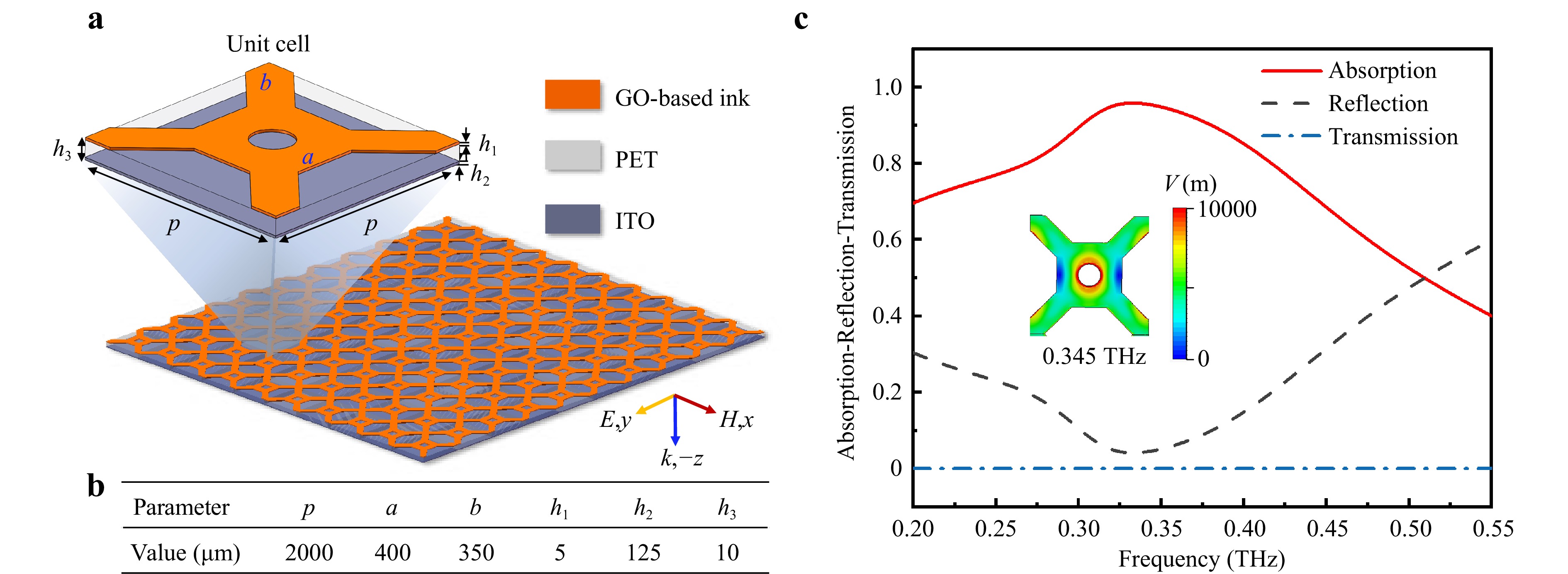
Fig. 7 a Schematic of the periodic cell array and the key dimensional parameters of the unit cell structure. b Size diagram of the PET-based metasurface absorber unit. c Simulated result of the PET-based metasurface absorber.
In addition, we designed a metasurface filter with a centre frequency of 0.8 THz. The structure of the filter is shown in Fig. 8a and consists of a grid pattern formed by perpendicularly crossed lines on the PET substrate. The specific structural parameters are shown in Fig. 8b. The background material is set to air with a dielectric constant of 1; the sheet resistance of the structural layer is set to 3 Ω·sq−1; and the dielectric constant of PET is set to 3.2. The optimised simulation results are presented in Fig. 8c. The results indicated that the transmission exceeded 90% at 0.748~0.848 THz and reached a peak of 93.1% at 0.8 THz. An analysis of the electric field distribution of the filter at 0.8 THz, it shows that strong electric fields were primarily concentrated along the inner edges of the grid cells, indicating that the transmission was caused by resonance within the grid cells.
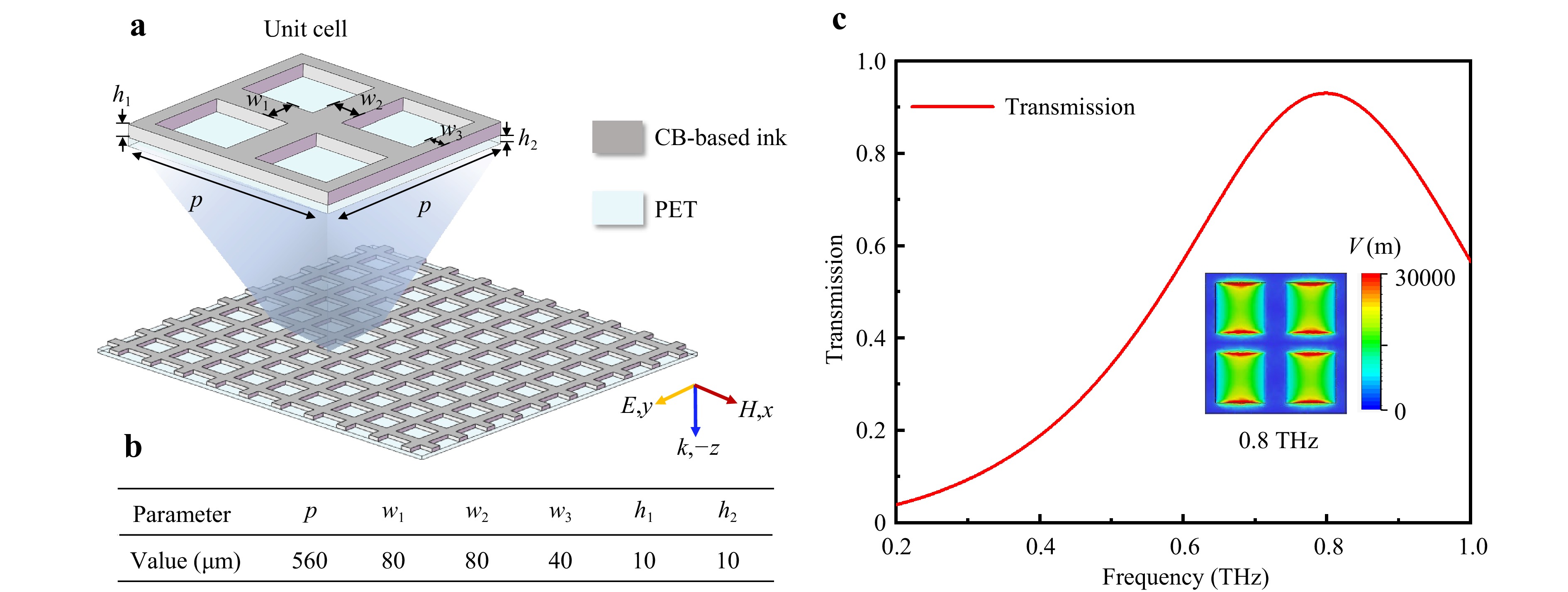
Fig. 8 a Schematic of the periodic cell array and the key dimensional parameters of the unit cell structure. b Size diagram of the metasurface filter unit. c Simulated transmission and electric field distribution.
-
Following this design, metasurfaces were fabricated using carbon-based 3D printing technology. The relevant printing parameters are presented in Table S6 of supplementary document S4. For the paper-based metasurface absorber, graphene-based ink with a sheet resistance of 47.35 Ω·sq−1 was selected. Fig. 9a-c present a macroscopic photograph, micrograph, and bending-state picture of the paper-based metasurface, respectively. The sample has an area of 15 mm × 15 mm and a thickness of 213.5 μm. For the PET-based metasurface absorber, GO-based ink exhibiting a sheet resistance of 149.2 Ω·sq−1 was selected. Fig. 9d-f present the corresponding macroscopic photographs, micrographs, and bending-state images, respectively. The samples had an area of 20 mm × 20 mm and a thickness of 128.2 μm.
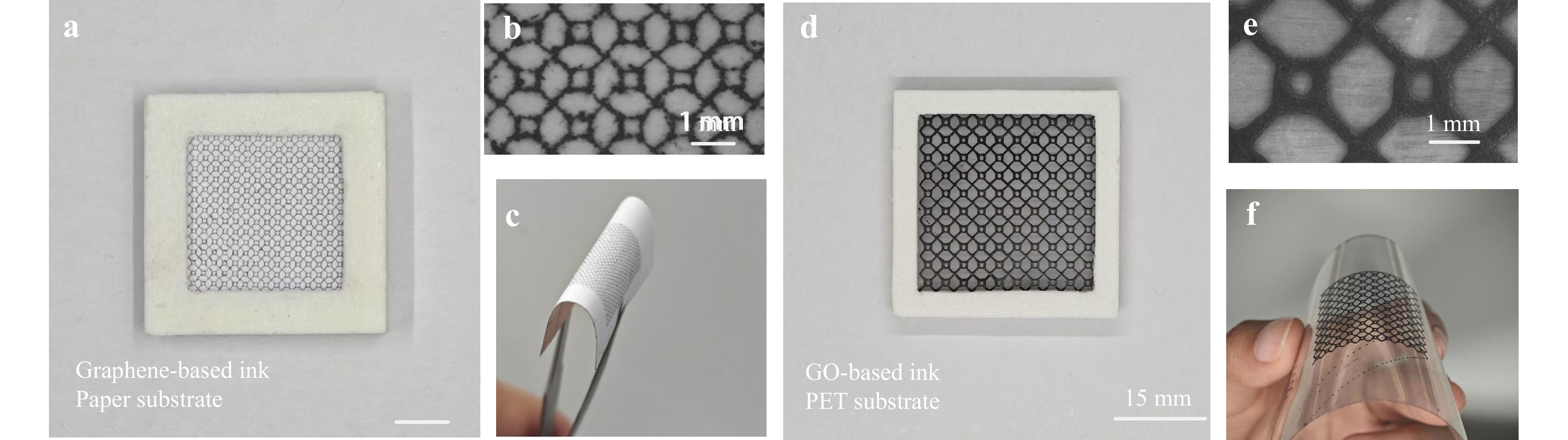
Fig. 9 Photographs of the paper-based metasurface absorber: a Macroscopic photograph; b Micrograph of structure; c Bending state picture. Photographs of the PET-based metasurface absorber: d Macroscopic photograph; e Micrograph of structure; f Bending state picture.
The E-jet mode is used to fabricate the metasurface filter with CB-based ink printing on a PET film of 10 μm thick. Since the sheet resistance of the ink was set to 3 Ω·sq−1 in the simulation, high-conductivity nano-silver paste was added in the CB-based ink to adjust the sheet resistance of the ink to 2.97 Ω·sq−1. The samples are shown in Fig. 10a-c. It had an area of 15 mm × 15 mm and a thickness of 18.4 μm.
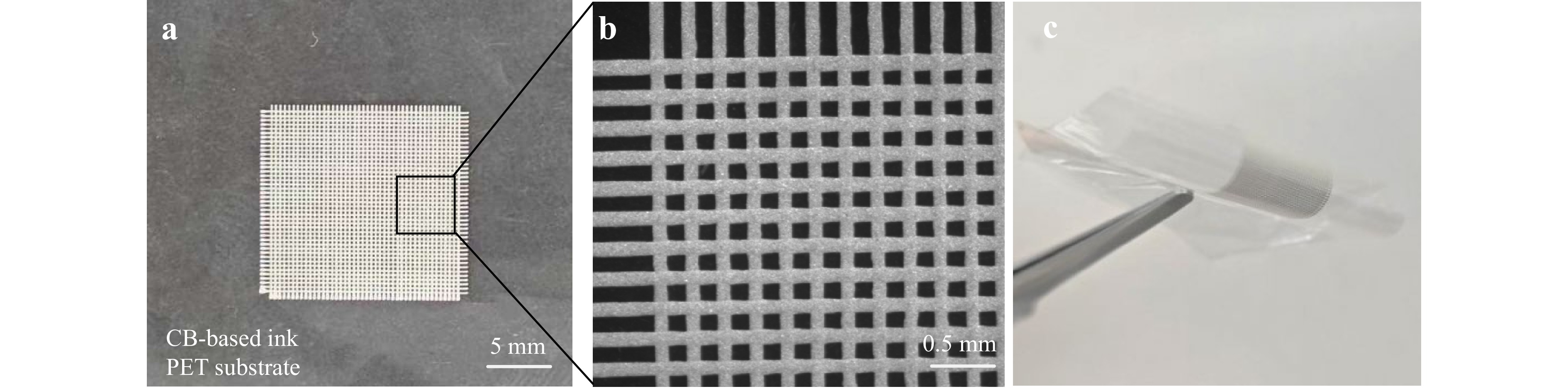
Fig. 10 Photographs of metasurface filter: a Macroscopic photograph; b Micrograph; c Bending state picture.
Subsequently, a fibre-based THz time-domain spectroscopy system (THz-TDS) was constructed to measure the spectra of the samples. As illustrated in Fig. 11, the THz-TDS system operates in two measurement configurations: transmission and reflection modes. In the transmission measurement mode (Fig. 11a), the femtosecond laser beam was divided into two beams. One beam, as the pump light, is incident on the THz antenna at the transmitting end to generate THz waves, and the other beam, as the detecting light, is incident on the THz antenna at the detecting end to detect THz pulses. The transmitting antenna radiates THz waves, which are collimated by an off-axis parabolic mirror. Then, the THz wave passes through the sample and is focused by the second off-axis parabolic mirror so that the receiving antenna receives THz signals. Using this system, the transmission of samples can be measured.
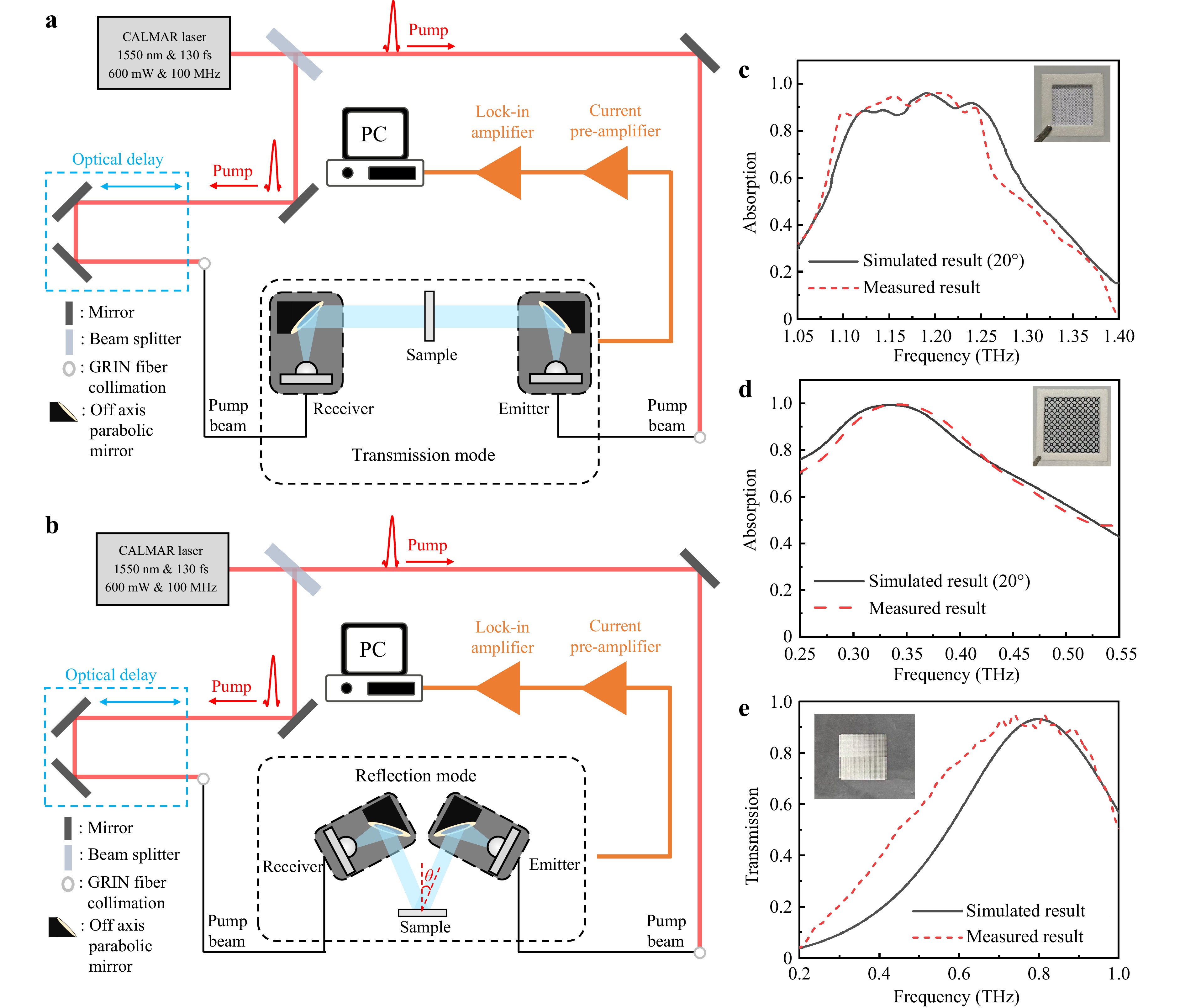
Fig. 11 a Schematic of the transmission spectrum measurement. b Schematic of the reflection spectrum measurement. c Absorption spectra of the paper-based metasurface absorber. d Absorption spectra of the PET-based metasurface absorber. e Transmission spectra of the metasurface filter.
The optical fibre provides flexibility to adjust the optical path; thus, the angle of the THz transmitter and receiver of the THz-TDS can be adjusted at will. The transmission measurement mode could be adjusted to the reflection measurement mode, as shown in Fig. 11b. The THz wave collimated by the off-axis parabolic mirror was reflected by the sample. The reflected light is focused by a second off-axis parabolic mirror to ensure that the receiving antenna receives the signal. Therefore, the reflection of the samples can be measured and the absorbance can be obtained. To ensure the reliability of the data, there are two steps to measure the absorption spectrum: 1) measuring the reference mirror with near 100% reflectivity (gold reflector) as the reference spectrum Rref, and 2) measuring the metasurface sample as the signal spectrum Rsam. The absorption spectrum can be calculated as:
$$ \text{A}=\frac{{R}_{\rm{ref}}-{R}_{\rm{sam}}}{{R}_{\rm{ref}}} $$ (3) Fig. 11c, d show the absorption spectra of the paper-based and PET-based metasurface absorbers, respectively. Because the incident angle of the THz wave in the experiment was 20°, the simulated absorption presented here was at an incident angle of 20°. The measured results show that the paper-based absorber achieves more than 90% absorption at 1.12~1.245 THz; the PET-based absorber achieves more than 90% absorption at 0.295~0.39 THz.
The measured results for the PET-based absorber were consistent with the simulated results. The paper-based absorber exhibited a broader absorption bandwidth than the simulated results. We believe that one of the reasons for this is the error generated during the printing process; paper exhibits a higher roughness than PET owing to its fibrous structure. When paper fibres are tangled, they create voids, allowing inks to seep in and produce a feathering effect. This caused the resonance structure to become more complex, introducing more resonance absorption peaks and broadening the bandwidth. The roughness of the substrates was measured and the ink penetration morphology was analysed, as shown in Supplementary Document S5. However, this effect is difficult to simulate using electromagnetic simulation software, leading to discrepancies between the simulation and experiment.
The transmission of the metasurface filter was measured in the THz-TDS transmission mode, and the results are shown in Fig. 11e. It achieved 92.4% at 0.8 THz. The measured results are generally consistent with the simulated results, except that the absorption bandwidth is broader compared to the simulation. Based on the analysis, we attribute this discrepancy to two reasons: 1) the thickness of the printed structural layer is smaller than that of the simulation, and 2) distortions at the line intersections due to the surface tension of the ink. Additionally, the electromagnetic characteristics of the three metasurfaces at different incident angles are analysed in S6.
Carbon-based manufacturing offers a faster, simpler, and more cost-effective route for fabricating carbon-based THz metamaterials than typical semiconductor processes. Its low equipment investment facilitates large-scale production, and its short preparation cycles make it ideal for rapid iterations. Furthermore, this technology can achieve a performance comparable to that of existing THz-printed devices and offers advantages such as dual-mode, compact size, and high integration. The relevant content is described in detail in the supplementary document (S7).
-
We proposed a carbon-based manufacturing approach for flexible THz metasurfaces. By designing carbon nanocomposite inks and a direct-writing printing head driven by high-precision stepper motors, two switchable printing modes of the inkjet and E-jet were realised so that the subwavelength resonance pattern of metasurfaces could be directly printed on flexible substrates. To verify the effectiveness of the carbon-based manufacturing method, the preparation process of the carbon nanomaterial ink and the configuration of the printing parameters were introduced. Furthermore, two THz metasurface absorbers and a metasurface filter composed of different carbon materials were designed, simulated, and fabricated on flexible paper and PET substrates. This paper is eco-friendly and inexpensive, and PET excels in tensile strength and transparency for diverse applications. The spectral test results for the metasurfaces were consistent with the expectations. Consequently, we believe that the carbon-based additive manufacturing method and flexible metasurfaces can serve as promising platforms for the development of advanced and specific devices for a wider range of THz applications, especially in fields such as laboratory verification and low-cost rapid manufacturing.
-
To prepare a high-performance printable conductive ink, terpineol and absolute ethanol were selected as the composite solvent systems. First, the solvents were mixed and stirred to form a uniform viscous phase, and then, different proportions of carbon nanomaterials were added. Stable nanomaterial suspensions were obtained via ultrasonic dispersion (760 W, 1 h). Finally, a polyester resin was added as an adhesive, and the viscosity of the system was dynamically adjusted using terpineol. (See details in S1: Preparation of carbon-based ink).
-
The preliminarily mixed carbon-based ink was further processed by ice-bath ultrasonication combined with mechanical stirring for one hour. After that, the resulting inks were moulded into 30 × 8 × 0.01 mm block samples and sintered at 120 ℃ for 15 min (supplementary document S8) as shown in Fig. 2b-d. Finally, a four-point probe resistance meter was used to measure the sheet resistances of the samples.
-
Sample morphology was observed using a Nikon SMZ1000 Greenough stereomicroscope (Japan) equipped with a white LED ring light source illumination system. Imaging was performed using a 1 × flat field apochromatic objective (Plan Apo 1 ×, WD 70 mm, Nikon) with a total system magnification of 8 ×, and images were acquired by a CMOS camera (Allied Vision Guppy Pro F503B, resolution 2,588 × 1,940 pixels). Statistical analyses of the characteristic linewidths are provided in Supplementary Document S9 to evaluate the repeatability and uniformity of the printed patterns. In addition, analyses of the adhesion and conductivity of the printed pattern under bending conditions are described in Supplementary document S10.
-
The authors extend sincere gratitude to the reviewers for their assistance and support.
Carbon-based manufacturing for flexible terahertz metasurfaces
- Light: Advanced Manufacturing , Article number: 95 (2026)
- Received: 27 October 2025
- Revised: 06 June 2026
- Accepted: 08 June 2026 Published online: 18 September 2026
doi: https://doi.org/10.37188/lam.2026.095
Abstract: Carbon materials have significant scientific and application potential in the terahertz field. Metasurfaces are considered the core components of next-generation of terahertz photonic systems. The introduction of advanced carbon-based fabrication techniques operating with high efficiency and low complexity is essential for the development of terahertz metasurface photonic devices. In this study, we demonstrate a carbon-based manufacturing approach. This relies on a dual-mode additive manufacturing technique and can be used to directly print subwavelength resonant structures on flexible substrates. We demonstrate the preparation method and properties of different carbon nanocomposite inks. In addition, we present printing parameter configurations and printing results. To demonstrate their effectiveness, two carbon-based metasurface terahertz absorbers and a terahertz filter are designed and fabricated. The resonant structures are printed directly onto different flexible substrates using different printing modes. A fibre-based terahertz spectroscopy system is built to test the samples. The test results meet the expectations and are consistent with the simulations. By enabling the low complexity of carbon-based additive manufacturing and offering flexibility in flexible substrate choice and resonant-pattern design, the approach could facilitate terahertz metasurface technologies for real-world applications.
Research Summary
Carbon-based manufacturing for flexible terahertz metasurfaces
Terahertz metasurfaces are considered the core components of next-generation of photonics, and carbon materials have significant potential in the field. Therefore, the introduction of advanced carbon-based fabrication techniques is essential for the development of terahertz metasurface devices. Cheng Gong from Nankai University and colleagues now report a dual-mode additive manufacturing technique that can be used to directly print carbon-based sub-wavelength resonant structures on different flexible substrates, thereby efficiently constructing terahertz flexible metasurfaces. The team demonstrated several applications for the manufacturing method including a Graphene-based broadband absorber, a GO-based metasurface absorber, and a CB-based filter, which proved that it can be used as a flexible, efficient and promising platform for developing advanced terahertz photonic devices.
Rights and permissions
Open Access This article is licensed under a Creative Commons Attribution 4.0 International License, which permits use, sharing, adaptation, distribution and reproduction in any medium or format, as long as you give appropriate credit to the original author(s) and the source, provide a link to the Creative Commons license, and indicate if changes were made. The images or other third party material in this article are included in the article′s Creative Commons license, unless indicated otherwise in a credit line to the material. If material is not included in the article′s Creative Commons license and your intended use is not permitted by statutory regulation or exceeds the permitted use, you will need to obtain permission directly from the copyright holder. To view a copy of this license, visit http://creativecommons.org/licenses/by/4.0/.

 DownLoad: