






-
Silicon photonics, with its unique compatibility with mature microelectronic manufacturing processes1,2, has emerged as a promising platform for chip-scale telecommunications, optical computing, and sensing applications3–5. However, in the near-infrared band, the heterogeneous integration of various emerging photonic materials on silicon platforms remains a key challenge in nanotechnology6–8. First, conventional photonic chips generally adopt a discrete architectural design for lasers and optical signal processing devices9–11. Integration of III-V lasers with silicon integrated circuits imposes stringent requirements on the alignment precision during the assembly process12–15. Second, although certain schemes have achieved the integration of III-V devices with silicon waveguides, their single-waveguide architectures still lack complex information processing capabilities owing to the absence of dedicated optical computing devices and on-chip processors16,17. Third, conventional on-chip processors are predominantly exemplified by configurations such as directional couplers (DC), Mach-Zehnder interferometers (MZI), and micro-ring resonators (MRR) connected by waveguides, which have two main shortcomings18–23. One is the large foot print, approaching tens-of-micrometres, of individual devices; the other is the large inter-component separation of tens to hundreds of micrometres required by electrically or thermally tuned traditional modulators to avoid crosstalk21–27.
In this study, we propose three strategies to address these challenges. First, III-V semiconductors with direct bandgaps are ideal materials for fabricating light-emitting devices in the near-infrared band, and whispering gallery mode (WGM) micro-lasers exhibit prominent advantages such as high quality, small size, and deterministic phase of the optical signal28–32. Second, the refractive-index modulation induced by nonlinear optical effects enables efficient optical tuning. The integration of nonlinear materials with silicon-based integrated devices enables all-optical signal modulation without the need for bulky electrode structures33–35. Furthermore, the incorporation of nonlinear materials creates additional opportunities for optimising the overall performance of the integrated photonic devices36–38. Third, the inverse design method has been applied to the design of connections between devices, such as beam splitters and waveguide crossings, which further reduces the chip footprint and enhances the integration density39–43.
With the joint utilisation of these three schemes, we propose and experimentally realise an ultracompact integrated photonic logic chip in the near-infrared band. The circuit is composed of active and passive parts that can achieve on-chip optical signal generation, transmission, and processing, as shown in Fig. 1a. The active part is implemented using a WGM micro-laser, and the passive part is an ultracompact silicon photonic chip. The laser is interconnected with the silicon photonic chip through end-to-end joint coupling, and outputs different intensities when implementing different currents. In the present study, this laser-chip interface serves as a proof-of-concept integrated optical source for system-level validation. The passive part is composed of silicon configurations including hybrid Bi2Te3-Si structures and inverse-designed structures with an inter-component separation distance of only 1.5 μm. We carefully constructed two types of hybrid Bi2Te3-Si micro-ring resonators, which are the anti-parity-time-symmetric (anti-PT-symmetric) resonators and 1/4-perimeter coated resonators, as shown in Fig. 1b. The anti-PT-symmetric resonators exhibit more pronounced resonance peak shifts before and after pumping. When combined with the wavelength selectivity of the 1/4-perimeter coated resonators, the photonic integrated chip realises different logical outputs when the WGM micro-laser is implemented with different currents and pumps distinct hybrid Bi2Te3-Si resonators, as shown in Fig. 1c. Compared to previously reported integrated optical logic devices44–48, the present architecture emphasises the joint realisation of source-to-chip integration, nonlinear resonator-based logic response, and inverse-designed ultracompact interconnects within a single on-chip platform, thereby addressing both functional integration and integration density. A comparison of the integrated optical logic devices is presented in Supplementary Materials S5.
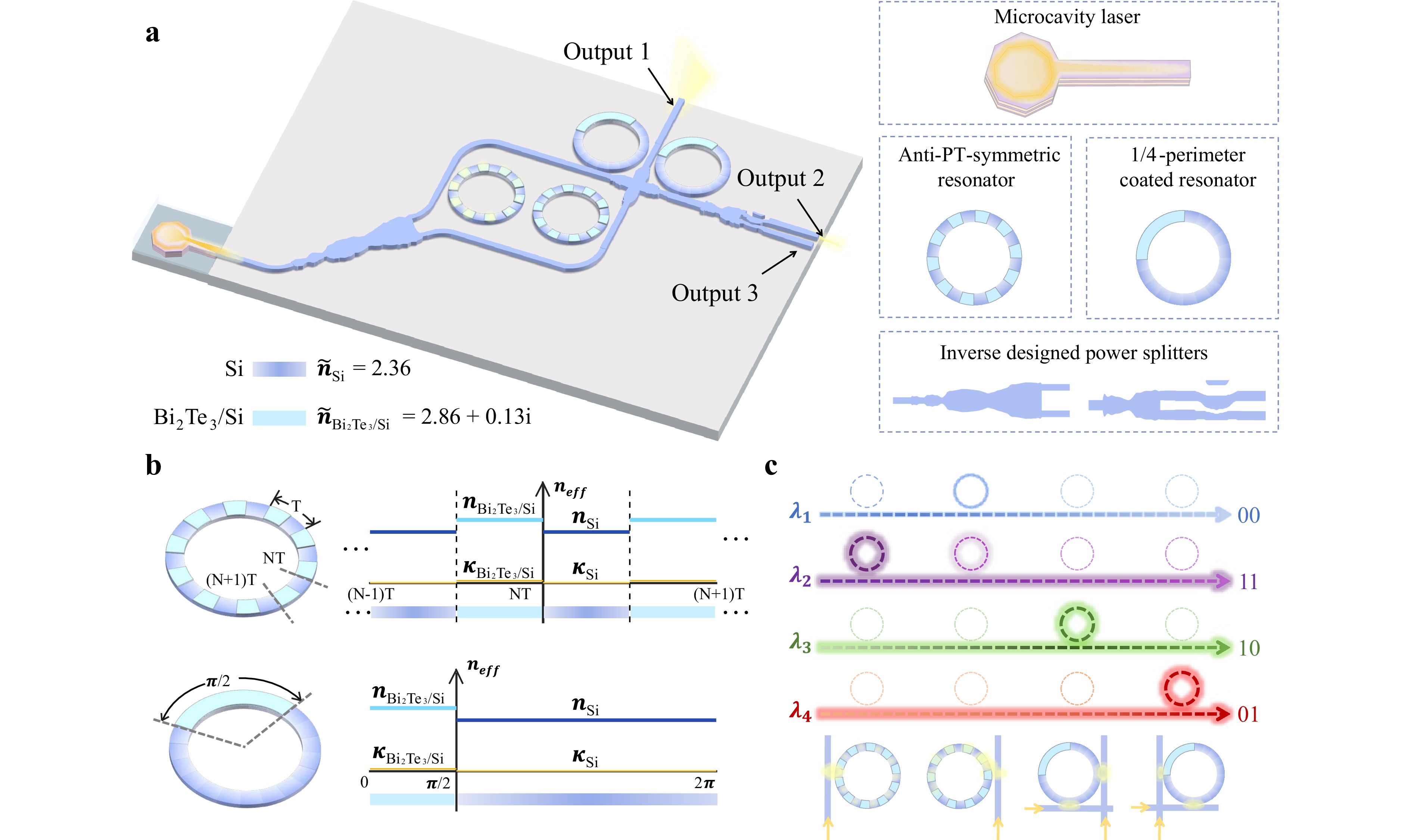
Fig. 1 Schemes of the proposed integrated photonic chip. a Scheme of the integrated chip composed of a microcavity laser, four micro-ring resonators, and inverse-designed beam splitters. b Two types of hybrid Bi2Te3-Si micro-ring resonators and their respective equivalent refractive-index distributions. The upper one corresponds to the anti-PT-symmetric resonator, whereas the lower one refers to the 1/4-perimeter coated resonators. c Functional schematic of the integrated chip. Under different laser-driving conditions, the input light delivered to the chip exhibits different operating states that interact differently with the four hybrid resonators. Distinct output states can be obtained owing to the resonance selectivity of the resonators and the nonlinear refractive index modulation provided by Bi2Te3.
-
A 51-order periodic structure is introduced onto a Si micro-ring resonator to construct an anti-PT-symmetric optical system, where breaking the symmetry leads to a more efficient mode selection and more obvious optical tuning compared to the ordinary resonator configuration. Along the circumference of the ring resonator, we spatially and periodically covered the nonlinear material Bi2Te3 to artificially construct a refractive index profile that follows the principle of anti-PT symmetry, as shown in Fig. 1b. The alternately arranged bare Si and hybrid Bi2Te3-Si structures form an anti-PT-symmetric system, and there are two standing eigenmodes in this system which suffer spontaneous symmetry breaking and possess staggered field distributions in the micro-ring resonator. The hybrid Bi2Te3-Si resonator supports two resonant modes, namely Mode A and Mode B, with distinct wavelengths. For Mode A at about 1,543.6 nm ($ {\lambda }_{a} $), the field is mostly confined within the hybrid Bi2Te3-Si regions whereas for Mode B at about 1,544.6 nm ($ {\lambda }_{b} $), the field is mostly confined within the bare Si regions. For the hybrid Bi2Te3 -Si resonator, the effective index of the transverse-electric (TE) mode in the waveguide varies periodically from 2.36 (bare Si) to 2.86 + 0.13i (hybrid Bi2Te3-Si) and the imaginary part stems from the nonlinear absorption effect of the Bi2Te3 coated on the waveguide. Detailed mode-field distributions in the bare Si waveguide and hybrid Bi2Te3-Si waveguide are shown in Supplementary Materials S3. The antinodes of Mode B are mainly distributed in the bare Si region, and the nonlinear material is present at the wave belly distributed in the field; therefore, the energy absorption of Mode B is much lower than that of Mode A.
We employed the finite-difference time-domain method to simulate the resonance characteristics of the anti-PT-symmetric resonator and obtained its transmission spectra under different pumping intensities, as shown in Fig. 2a. In the absence of applied pumping, these two modes split in the resonator. When pumping is applied, Mode A and Mode B degenerate to form a single deeper dip at $ {\lambda }_{b} $. As the pumping power increases, the nonlinear effect becomes more pronounced, leading to a significant shift in the resonance wavelength from $ {\lambda }_{b}\rightarrow {\lambda }_{b}' $. The red-shifted dip in the transmission spectra as the pumping intensity increases occurs because Bi2Te3 exhibits a Kerr nonlinear effect with a positive nonlinear coefficient ($ {n}_{2}> 0 $); according to the relationship $ n={n}_{0}+{n}_{2}I $, the refractive index of Bi2Te3 $ n $ increases as the pump intensity $ I $ increases, leading to an increase in the effective optical path and a redshift of the dip in the transmission spectrum. When the resonance wavelength is $ {\lambda }_{b} $, the antinodes and nodes of the resonator exactly correspond to the geometric length and period of the micro-ring, resulting in the highest coupling efficiency and the deepest dip in the transmission spectrum. With the redshift of the resonance dip, the coupling efficiency of the resonator decreases, and the dips in the transmission spectrum become shallower.
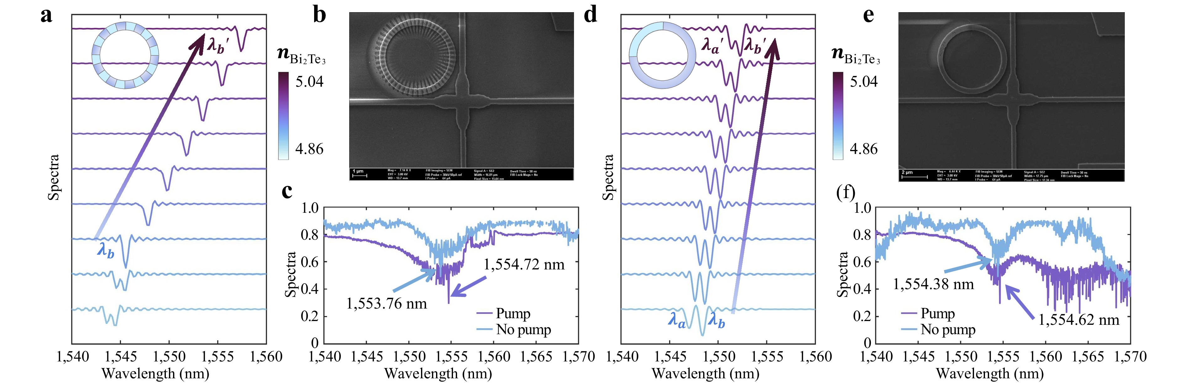
Fig. 2 Theoretical and experimental results of hybrid Bi2Te3-Si micro-ring resonators hybrid Bi2Te3 micro-ring resonator. The anti-PT symmetric resonator: a Transmission spectra and resonance wavelength shifts for different pumping intensities. In the absence of pumping two split resonant modes exist in the micro-ring, Mode A at 1,543.6 nm ($ {\lambda }_{a} $) and Mode B at 1,544.6 nm ($ {\lambda }_{b} $). When pumping is applied, these two modes become degenerate resulting in significant decrease in the dips of the transmission spectrum at 1,545.6 nm ($ {\lambda }_{b} $). The redshifted dip is at 1,557.4 nm ($ {\lambda }_{b}' $) with strong pump. b SEM photo of the anti-PT-symmetric resonator. c Experimentally measured transmission spectra. When pumped, the resonant wavelength is redshifted by 1 nm. Micro-ring resonators with 1/4-perimeter coated: d Transmission spectra and resonance wavelength shifts under different pumping intensities. In the absence of pumping the two split resonant modes are Mode A at 1,547.0 nm ($ {\lambda }_{a} $) and Mode B at 1,548.4 nm ($ {\lambda }_{b} $). When pumping is applied, the degenerate mode is at 1,551.4 nm ($ {\lambda }_{a}' $). The redshifted dip is at 1,552.3 nm ($ {\lambda }_{b}' $) with strong pump. e SEM image of the anti-PT-symmetric resonator. f Experimentally measured transmission spectra. When pumped, the resonant wavelength is redshifted by 0.24 nm.
To achieve a suitable line width of the resonant peak, large enough to ensure the multi-function of the integrated chip, the radius of the micro-ring chosen to be 2.5 μm. For a given micro-ring radius, the higher the azimuthal order of the mode along the micro-ring, the shorter the wavelength. Selecting the 51st-order eigenmode places the resonance wavelength in the near-infrared band. Subsequently, we adjusted the length ratio of the bare Si and hybrid Bi2Te3-Si in each period to ensure that the optical paths of each segment were equal; thus, the nodes and antinodes of the standing-wave eigenmodes were completely located in one of the regions. Finally, the length ratio of the hybrid Bi2Te3-Si to the entire selected period was 0.47. The scanning electron microscopy (SEM) image of the anti-PT symmetric resonator is shown in Fig. 2b. The results of the experimental measurements before and after pumping are shown in Fig. 2c, the refractive index of the upper Bi2Te3 layer changes from 4.86 to 5.04 and the transmission peak redshifts from 1,553.76 nm to 1,554.72 nm.
Subsequently, the nonlinear material Bi2Te3 is coated onto a quarter of the ring, as shown in Fig. 2e, and the characteristics of this 1/4-perimeter coated micro-ring resonator under pumping conditions are numerically simulated. With increasing pumping intensity, the refractive index of the nonlinear material Bi2Te3 changes. The transmission spectrum of the normal hybrid Bi2Te3-Si resonator is shown in Fig. 2d. There are also two resonant modes Mode A and Mode B in the micro-ring; however, unlike in the anti-PT-symmetric resonator, owing to the poor symmetry of the two modes when passing through the hybrid Bi2Te3-Si region, the resonant modes cannot degenerate under certain conditions. In the anti-PT-symmetric resonator, degeneracy of the two directional modes can be readily realized under appropriate pumping conditions. However, because the application of pumping induces a change in the refractive index of Bi2Te3, the redshift in the transmission spectrum of the normal hybrid Bi2Te3-Si resonator is much smaller than that of the anti-PT-symmetric resonator. In the experiment, the measured transmission peak redshifts from 1,554.38 nm (before pumping) to 1,554.62 nm (after pumping) as shown in Fig. 2f, which is smaller than the 1 nm redshift of the transmission peak of the anti-PT-symmetric resonator.
-
We constructed an integrated photonic chip using anti-PT-symmetric resonators as the key components. In our scheme, an inverse design method was adopted to reduce the area of the connecting devices and improve the integration density. The detailed algorithms for the inverse design and performance characterisation of the inverse-designed devices are explained in Supplementary Materials S1.
A pump-probe experiment is conducted to characterise the nonlinear optical response of the Bi2Te3 thin-film and hybrid Bi2Te3-Si devices, and the experimental setup configuration is shown in Fig. 3a. A tuneable laser (wavelength tuneable in the range of 1,500–1,600 nm) is employed, and the light from the laser is split into two beams using a beam splitter as the pump and probe lights. A pump light is used to excite the nonlinear effect of the Bi2Te3 thin film, whereas a probe light is used to monitor the transient change in the transmission spectrum. The wavelength of the pump laser is locked at the linear resonance wavelength of the target mode when measuring the hybrid Bi2Te3-Si resonator. A mechanical delay line is inserted into the pump light path to adjust the time delay between the pump and probe pulses to within a delay range of 0–500 ps, to cover the transient relaxation process of the material.
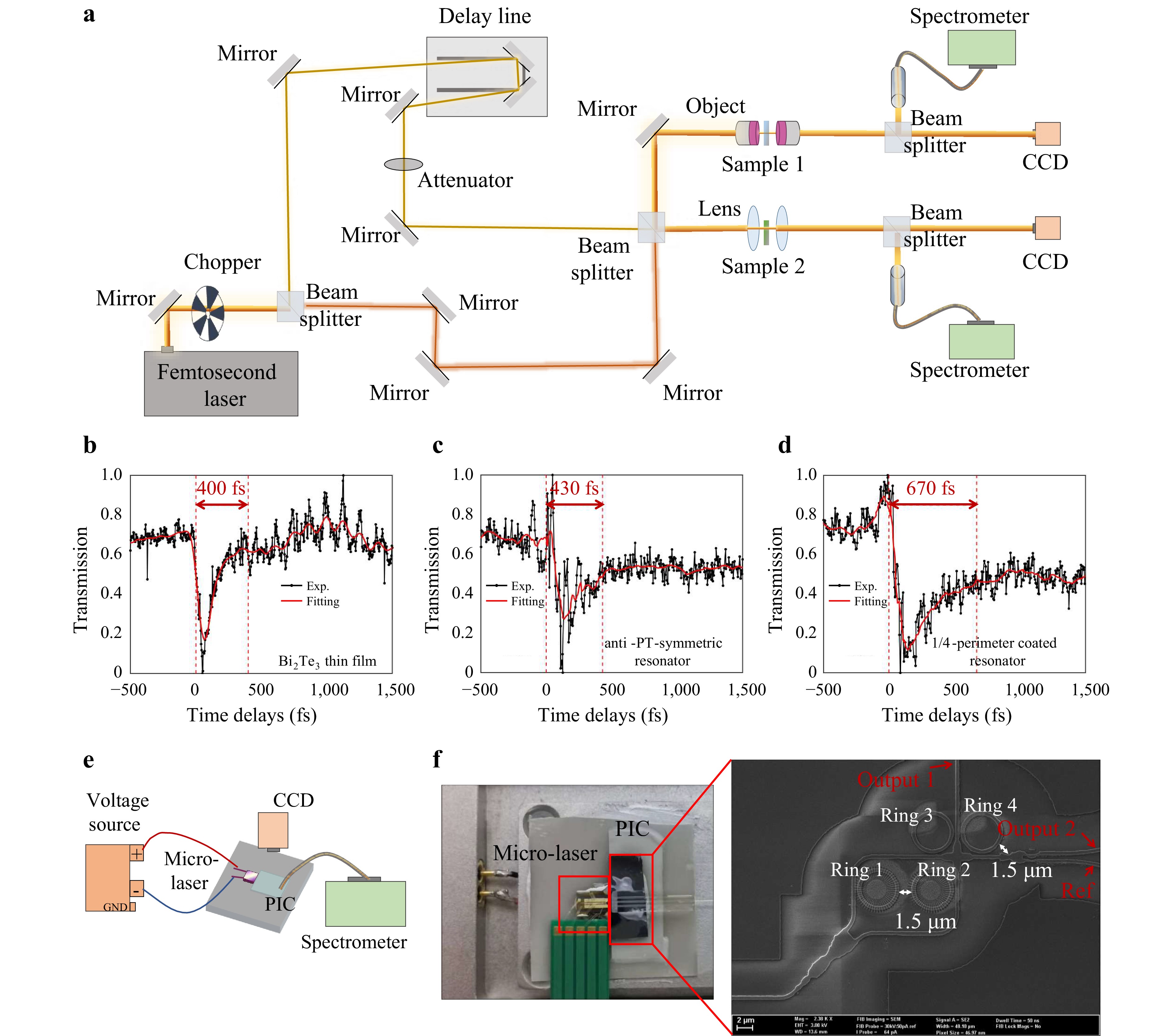
Fig. 3 Experiment realization of the hybrid integrated Bi2Te3-Si photonic chip. a The pump-probe beam path. b Pump-probe delay curve of the Bi2Te3 thin film, showing an intrinsic transient response time of ~400 fs. c Pump-probe delay curve of the anti-PT-symmetric hybrid resonator, showing an effective device response time of ~430 fs. d Pump-probe delay curve of the 1/4-perimeter coated hybrid resonator, showing an effective device response time of ~670 fs. e The optical fibre coupling system for the measurement of the PIC. f The camera image of packing chip. On the left is the micro-laser and on the right is the passive circuit.
Sample 1 comprises the on-chip hybrid Bi2Te3-Si devices. For this sample, a high-magnification objective lens is used to collimate and focus the incident light, with the focused beam spot impinging on the input grating coupler of the on-chip sample. The transmitted light of the on-chip hybrid Bi2Te3-Si device is coupled to a single-mode fibre using another objective lens. The light signal is subsequently transmitted to a spectrometer and a CCD camera for measurement. The measured intensity spectra of the probe light are shown in Fig. 2c, f. The time-delay curves of the anti-PT symmetric resonator and 1/4-perimeter coated micro-ring resonator are shown in Fig. 3c, d, respectively.
Sample 2 is the nonlinear Bi2Te3 thin-film sample. For this sample, lens groups are used to collimate and focus the light emitted by the laser. The focused beam spot is then incident on the sample, and the transmitted light of the thin-film sample is coupled to a single-mode fibre using another set of lens groups. The light signal is subsequently transmitted to a spectrometer and a CCD camera. The time-delay curve is shown in Fig. 3b.
The delay extracted from the Bi2Te3 thin film characterizes the intrinsic ultrafast response of the Kerr nonlinear material, whereas the delay measured from the on-chip hybrid resonators represents the effective transient response of the device, which includes both material nonlinearity and cavity-assisted optical dynamics. When the photon lifetime of the micro-ring becomes comparable to or longer than the intrinsic material response time, the measured device response is increasingly influenced by the cavity dynamics. In this regard, the anti-PT-symmetric resonator with a relatively shorter photon lifetime operates close to the material-limited regime, whereas the 1/4-perimeter-coated resonator with a higher cavity Q factor and longer photon lifetime shows a more pronounced cavity lifetime contribution to the effective response. Overall, the hybrid resonators maintain an ultrafast transient operation, indicating that appropriate cavity Q engineering can balance the nonlinear enhancement and response speed. These results indicate that the proposed hybrid resonators are promising compact nonlinear building blocks for integrated photonic-logic applications.
The electrically driven and fibre-coupled detection configuration shown in Fig. 3e is constructed to characterize the proposed packaged device as shown in Fig. 3f, which consists of a voltage source, translation stage, CCD camera, an objective lens, and a coupling fibre. The on-chip laser is electrically driven by a voltage source to generate an optical signal. The emitted light propagates through the photonic chip and exits from the output grating couplers, where it is coupled to an optical fibre. The output signal is then analysed using an optical spectrum analyser to obtain the transmission spectrum of the chip under the given electrical driving conditions of the integrated micro-laser. The electrically driven laser serves as an integrated optical source for the system-level characterisation of the packaged chip. The observed spectral evolution is consistent with the nonlinear refractive index modulation in the hybrid Bi2Te3-Si micro-ring resonators, together with the resonance selectivity of the integrated circuit. Different driving conditions produce different chip output states, as shown in Fig. 4i, l, demonstrating the feasibility of on-chip signal generation, transmission, and logic processing in a hybrid integrated platform.
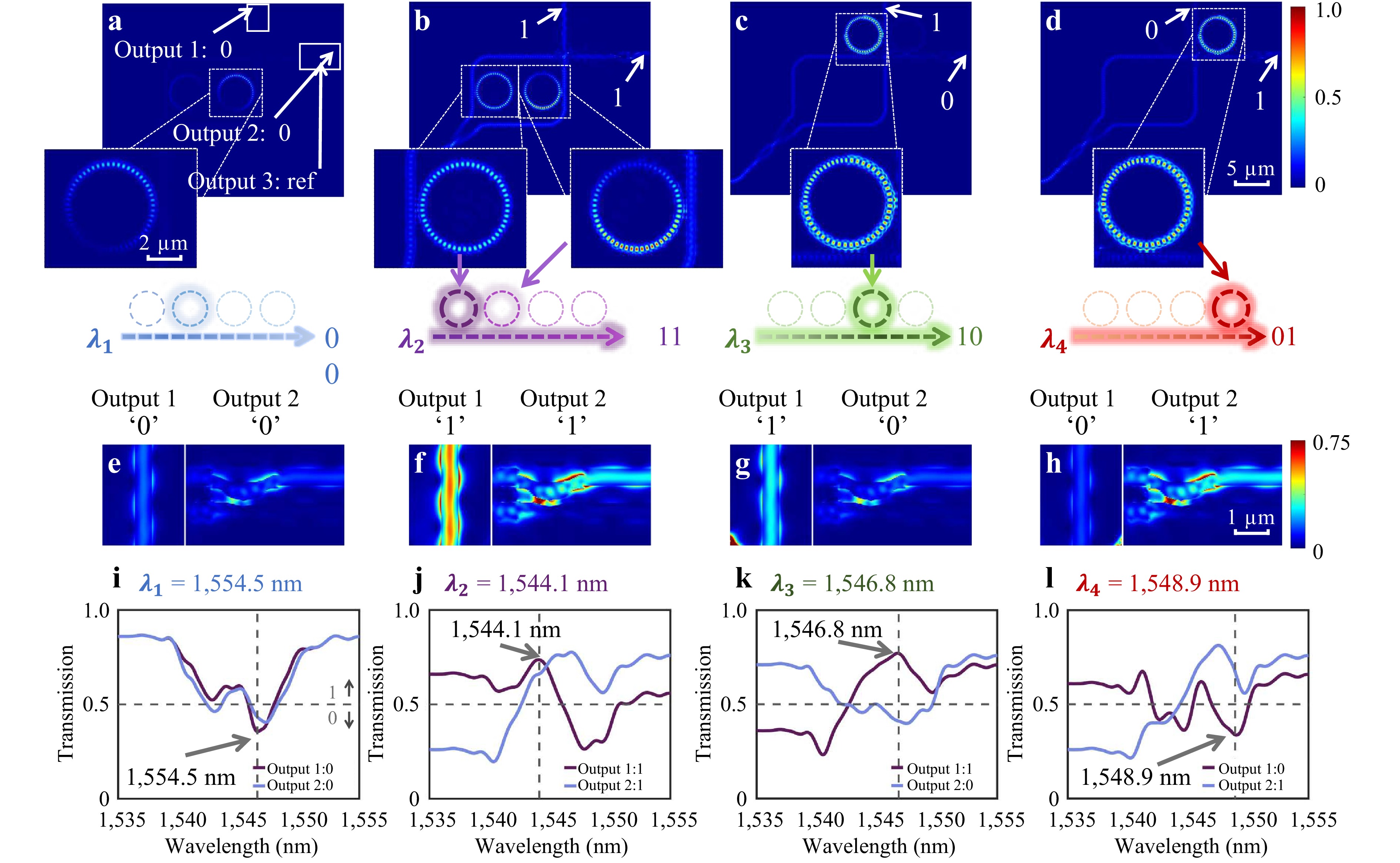
Fig. 4 Logic operations on the proposed photonic chip. a-d Field distribution of the photonic logic chip with logical outputs of ‘00’, ‘11’, ‘10’, ‘01’. e, f Field distribution at Output Port 1 and Output Port 2 with logical outputs of ‘00’, ‘11’, ‘10’, ‘01’. i-l Experimental measurement of transmission spectra with logical outputs of ‘00’, ‘11’, ‘10’, ‘01’.
-
We employed the finite-difference time-domain method to simulate the function of the entire optical logic chip and experimentally measured it under the given electrical-driving conditions of the integrated micro-laser. In the present experiment, the integrated III–V micro-laser serves as an on-chip optical source for a proof-of-concept demonstration of the logic functionality of the proposed photonic chip. By electrically driving the micro-laser, the logic functionality of the chip arises from the different responses of the four hybrid Bi2Te3-Si micro-ring resonators under different input conditions. These responses are associated with the resonance characteristics of the resonators and the Kerr nonlinear refractive index modulation introduced by the Bi2Te3 coating.
As shown in Fig. 4a, there are 3 output ports, two of which serve as the 2-bit logic operation outputs, and the other port is for reference. For Output Ports 1 and 2, we defined the wavelength at the dip of Port 1 as the effective operating wavelength. If the normalised transmission at this wavelength exceeds 50%, the output is ‘1’; if it is less than 50%, the output is ‘0’, as shown in Fig. 4i. The transmission at Output Port 3 after transmission through various on-chip devices and waveguides is taken as ‘0’ for reference; it is used as a baseline to verify the validity and contrast of the logical outputs at Ports 1 and 2. The corresponding transmission spectrum of Port 3 has been added to Supplementary Materials S4.
When the voltage applied to the micro-laser is low, no effective pump is added to the rings; Rings 1 and 2 exhibit weak resonant coupling at 1,554.5 nm, whereas Rings 3 and 4 do not exhibit resonant coupling, as shown in Fig. 4a, e. The normalised transmission of Output Ports 1 and 2 are 36% and 44%, respectively, resulting in a logical output of ‘00’, as shown in Fig. 4i. When the voltage applied to the micro-laser is adjusted to the corresponding operating state, Ring 1 exhibits enhanced coupling at the selected wavelength of 1,544.1 nm, Ring 2 exhibits weak resonant coupling, and Ring 3 and Ring 4 do not exhibit resonant coupling, as shown in Fig. 4b, f. The normalised transmission of Output Ports 1 and 2 increased to 74% and 66%, respectively, with a logical output of ‘11’, as shown in Fig. 4j. Similarly, as the voltage applied to the micro-laser increases and the input condition is adjusted to the corresponding operating state of Ring 3, its resonance is dynamically shifted to an operating wavelength of 1,546.8 nm, whereas Rings 1, 2, and 4 are not in resonant coupling, as shown in Fig. 4c, g. The normalised transmission of Output Ports 1 and 2 are 77% and 41%, respectively, giving a logical output of ‘10’, as shown in Fig. 4k. When the input condition is adjusted to the corresponding operating state of Ring 4, it exhibits strong resonant coupling at 1,548.9 nm, whereas Rings 1, 2, and 3 do not exhibit resonant coupling, as shown in Fig. 4d, h. The normalised transmission of Output Ports 1 and 2 are 34% and 68%, respectively, resulting in a logical output of ‘01’, as shown in Fig. 4l. Pump current in the range of 0–25 mA is applied to the laser to achieve intensity tuning in the wavelength range of 1,540 nm to 1,560 nm.
In all cases, the measured logic states originate from the distinct responses of the hybrid resonators under different input conditions. The observed transmission contrast is consistent with the resonance-dependent modulation in hybrid Bi2Te3-Si micro-ring resonators, where the Kerr-induced nonlinear refractive-index variation is expected to play an important role.
-
In summary, we experimentally demonstrated an ultracompact fully all-optical photonic integrated chip operating in the near-infrared band. The circuit integrates a WGM micro-laser, four hybrid Bi2Te3-Si micro-ring resonators (anti-PT-symmetric resonators and the 1/4-perimeter coated resonators), and inverse-designed interconnects, achieving an ultra-high integration density of 1.5 μm inter-component spacing and 2-bit all-optical logic operations. The WGM micro-laser provides a proof-of-concept integrated optical source and enables on-chip optical-signal generation. This study verified the feasibility of butt-coupled source integration for a hybrid logic-chip architecture under electrically driven operation. Further optimisation of the laser–chip coupling efficiency and long-term stability will be important in future studies. Pump-probe measurements indicate hundreds of femtosecond transient responses in the hybrid Bi2Te3-Si micro-ring resonators and the anti-PT-symmetric resonators, functionalized with Bi2Te3 Kerr nonlinearity-induced refractive index modulation and a mode degenerate mechanism, exhibit a 1 nm resonance redshift under pumping and achieve efficient all-optical tuning. The packaged-chip measurements verify the functionality of the integrated logic platform under electrically driven operation and the inverse-designed ultra-compact layout realises 2-bit outputs (‘00’, ‘11’, ‘10’, ‘01’) for logic operations.
Our study provides a novel technical approach for realising fully integrated photonic chips and offers insights into material engineering, inverse design, and mode manipulation of high-performance photonic chips. While the present work validates the feasibility of the proposed hybrid integrated architecture, several opportunities remain for further improvement. The heterogeneous integration process can be further optimized to enhance coupling efficiency and device stability. Incorporating suitable encapsulation strategies for the Bi2Te3 thin film could improve environmental and mechanical robustness by mitigating oxidation and delamination. In addition, although the current device demonstrates 2-bit all-optical logic operation as a proof of concept, scaling to higher-bit operations and more sophisticated photonic circuits will require advances in system-level integration and interconnect architectures. These developments will pave the way toward ultrafast and energy-efficient all-optical computing and communication systems.
-
We performed numerical simulations using the two-dimensional finite-element method and the two-dimensional finite-difference-time-domain method. The WGMs in the micro-cavity of the laser and the coupling modes in the hybrid Bi2Te3-Si micro-ring resonators are numerically computed to reveal their characteristics.
For the WGMs in the micro-cavity of the laser, we mainly focus on the TE modes owing to the TE-dominant gain in commonly used compressively stressed AlGaInAs/InP multiple quantum well (MQWs) epitaxial wafers. The refractive index of 3.2 for the micro-cavity is close to the effective refractive index of the TE modes in the MQWs wafer. A benzocyclobutene (BCB) layer with a refractive index of 1.54 is used to laterally confine the micro-cavity. A perfect matched layer (PML) absorbing boundary with a width of 1 μm is set to terminate the simulation window. The mode Q factors can be obtained as follows:
$$ Q=\frac{Re\left(\omega \right)}{\left| 2Im\left(\omega \right)\right| } $$ (1) where ω is the calculated complex mode frequency. To distinguish between the degenerate symmetric and anti-symmetric modes, we set the perfect electric conductor (PEC) and perfect magnetic conductor (PMC) conditions, respectively, along the symmetry axis of the micro-cavity. The symmetries of the modes are defined based on the symmetries of the amplitude distributions of the magnetic-field relative to one diagonal for the TE modes. A detailed characterisation of the WGM lasers is provided in Supplementary Materials S2. It should be noted that, in the present work, the integrated III-V micro-laser mainly serves as a proof-of-concept on-chip source for system-level validation of the hybrid logic chip. Although the butt-coupled laser-chip interface enables on-chip signal generation and logic-state readout, the coupling efficiency and long-term stability of this interface have not yet been fully optimised. Further improvements are expected from better balancing of the cavity output coupling with the intrinsic cavity loss and from engineering the output mode profile of the micro-laser for improved mode matching to the connected waveguide49,50.
The waveguides in the photonic integrated circuits are 220 nm thick and 500 nm wide and the thickness of the thin film Bi2Te3 on the Si waveguide is 50 nm. The numerical model adopts the same key geometrical parameters as the fabricated devices, including the silicon waveguide cross-section of 500 nm × 220 nm, the 50-nm-thick Bi2Te3 layer, and the experimentally designed hybrid resonator geometry. For the anti-PT-symmetric resonator, the simulated structure corresponds to the fabricated 2.5-μm-radius micro-ring and a hybrid-section/period-length ratio of 0.47. For the 1/4-perimeter coated micro-ring resonators, the simulated structure also corresponds to the fabricated 2.5-μm-radius micro-ring and the hybrid section is of 1/4-perimeter. The inverse-designed interconnects are also modelled with the same fabricated waveguide cross section, and their detailed geometrical dimensions and optimisation procedure are provided in Supplementary Materials S1.
For the hybrid Bi2Te3-Si micro-ring resonators, the effective refractive index of the fundamental TE mode in the pure silicon waveguide is 2.355, whereas the effective refractive index of the fundamental TE mode in the hybrid Bi2Te3-Si waveguide varies from 2.856 to 2.920, depending on the range of variation of the refractive index of Bi2Te3. The surrounding boundaries are also PML-absorbing. The mode profiles of the bare Si and hybrid Bi2Te3-Si waveguides are shown in Supplementary Materials S3. The electric-field distributions in the middle of the Si waveguide are investigated, as shown in Supplementary Materials S3, and the transmission spectra under different pumping conditions are investigated, as shown in Fig. 2a, d.
For the entire photonic logic chip, the simulation region is set to 40 µm × 28 µm with PML boundaries. The electric field distributions are shown in Figs. 4a, h.
-
We define the performance of our device as the overlapping integrals of the output mode fields and normalised target output modes in the cross-shaped output waveguide in the range of 1,530 nm-1,570 nm. The target output modes are predefined and remain unchanged during the optimisation process, as detailed in Supplementary Materials S1. The objective function is defined as follows:
$$ f=f\left(E\left(\varepsilon \right)\right)$$ (2) where $ E\left(\varepsilon \right) $ is the intensity distribution of propagation field and $ {\varepsilon }^{k} $is the permittivity of the $ kth $ iteration.
$$ {\varepsilon }^{k+1}={\varepsilon }^{k}+\alpha \frac{\partial f}{\partial {\varepsilon }^{k}} $$ (3) Second, the gradient $ \dfrac{\partial f}{\partial {\varepsilon }^{k}} $ can be calculated using the equation below:
$$ \frac{\partial f}{\partial {\varepsilon }^{k}}=\frac{\partial E}{\partial {\varepsilon }^{k}}\frac{\partial f}{\partial E} $$ (4) Then we can substitute $ \dfrac{\partial E}{\partial {\varepsilon }^{k}} $ for $ \mathrm{E} $, which is the propagation field intensity distribution of the original source over the designed section and $ \dfrac{\partial f}{\partial E} $ for $ \mathrm{E'} $, which is the propagation field distribution of adjoint source over the designed region51,52.
$$ \frac{\partial f}{\partial {\varepsilon }^{k}}=-{\omega }^{2}{\mu }_{0}{E}^{\text{'}}E $$ (5) where$ \omega $ is the frequency of the signal light, $ {\mu }_{0} $ is the vacuum permeability. $ {E}^{\text{'}} $ and $ E $ are the two-dimensional cross-sectional electric field distributions of the accompanying light and signal light, respectively. $ \dfrac{\partial f}{\partial {\varepsilon }^{k}} $ is derived from $ {E}^{\text{'}} $ and $ E $ to obtain the distribution of the dielectric constant of the $ ({k+1)}^{\text{th}} $ iteration. When the predetermined number of iterations is reached, $ \varepsilon $ tends to the set square value of the refractive index of Si or air, which is 3.48 or 1, respectively. The entire optimisation process can be divided into two steps: continuous and discrete. In the continuous optimisation process, we set the bias factor to be small, whereas in the discrete optimisation process, we set the bias factor to be large. The refractive index of each basic unit is optimised by using the bias factor $ \beta $, which is set to change the refractive index of each basic unit along the direction of the final gradient, and the speed and magnitude of the change of the refractive index are controlled according to the bias factor.
-
A passive photonic chip was fabricated on a silicon-on-insulator (SOI) wafer using standard contact photolithography and ICP techniques. We first clean the SOI piece (2 cm × 2 cm) at 70 °C in both DSF-2 and DQY-2 baths for 60 min. To fabricate the first layer, the integrated photonic devices and waveguides are defined by patterning a 250 nm ZEP-520A resist layer using a JEOL JBX-9500FS electron beam lithography system. The etching process for the silicon device layer uses an OXFORD PlasmaPro 100 Cobra 180. The etching depth is 220 nm. Then we strip resist in 70°C DQY-2 baths for 30 min. The etching depth of the second layer is 70 nm. For the third layer, the structure of the nonlinear material is defined by patterning a 250 nm ZEP-520A resist layer using a JEOL JBX-9500FS electron-beam lithography system. A 50-nm-thick Bi2Te3 film is deposited using the pulsed-laser-deposition (PLD) method. Then we strip resist in 70°C DQY-2 baths for 30 min, thereby forming the pre-patterned Bi2Te3 structures with well-defined microscale geometry. Focused ion beam (FIB) etching is introduced as the secondary patterning step to fabricate fine structures on the prepatterned circular Bi2Te3 layer, enabling nanoscale feature definition and accurate alignment with th e underlying silicon photonic structures. After the FIB process, a passive photonic structure is fabricated. Subsequently, we cut the sample at a specific position according to the pre-etched marks, end polish, and butt with a waveguide-output micro-laser. After the precise alignment of the laser and passive components, the laser is butt-coupled to the chip facet. The electrical and optical ports are then encapsulated to complete chip fabrication. In this study, a butt-coupled interface was implemented to verify the source-to-chip feasibility and packaged operation rather than to fully optimise the coupling efficiency or long-term coupling robustness. A complete fabrication flowchart for the photonic chip is shown in Supplementary Materials S1.4.
-
The circular-side octagon micro-laser with 8 μm-side-length waveguides is fabricated using a 2.5-inch AlGaInAs/InP epitaxial wafer. First, the epitaxial wafer is cleaned sequentially to remove surface contaminants. It is immersed in an acetone bath at 80 °C for five cycles, with a 5 min interval between each cycle. The wafer is then cleaned five times with room-temperature ethanol and rinsed thoroughly with deionised water. A 600 nm-thick SiO2 layer is deposited on the cleaned epitaxial wafer as a hard mask via plasma-enhanced chemical vapour deposition (PECVD) using SIS Ltd MultiplexCVD system. Prior to photolithography, hexamethyldisilazane (HMDS) is spin-coated as an adhesion promoter to enhance the bonding between the SiO2 mask and photoresist. The first photolithography step is performed using AZ6130 positive photoresist for the pattern transfer. After photolithography and development, inductively coupled plasma (ICP) etching is performed using an Oxford Instruments PlasmaLab System 100 at an etching depth of 470 nm. After etching, the residual SiO2 mask is removed by wet etching in a 1:10 dilute hydrofluoric acid (HF) solution. A 230 nm thick silicon nitride (SiN) protective layer is then grown on the wafer surface. Divinyl siloxane bis-benzocyclobutene (DVS-BCB; Dow Chemical Company CYCLOTENE 302-46) is used to fill the device trenches. The wafer is firstly spin-coated with 3 μm thick BCB and soft-cured for 3 h 40 min, then it is spin-coated with 2.8 μm thick BCB and hard-cured for 4 h. Subsequently, reactive ion etching (RIE) is used to etch the BCB layer until its surface is below the top surface of the SiN layer, and a second photolithography step is conducted to define the electrode windows. A 200 nm-thick SiO2 mask is then deposited via PECVD, followed by ICP etching of the SiO2 and SiN layers to a depth of 690 nm. Over-etching is performed to ensure complete removal of the SiO2 and SiN layers in the electrode window regions. For the third photolithography step, a 3 μm-thick photoresist is spin-coated onto the wafer. Without postexposure baking, a photoresist is developed to fully expose the electrode windows. The 150 nm-thick InP protective layer above the ohmic contact region is removed via electrochemical etching. P-type ohmic contact metals (Ti/Pt/Au) with thicknesses of 50 nm, 50 nm, and 300 nm, respectively, are deposited via electron beam evaporation, with the photoresist still in place (lift-off process). The photoresist is stripped by soaking the wafer in acetone for a certain period to yield patterned P-side electrodes. The epitaxial wafer is then thinned and polished to a substrate thickness of approximately 120 μm. In the fourth step, n-type ohmic contact metals (Ni/Ge/Au) are deposited on the N side of the wafer via magnetron sputtering, followed by annealing to form a good ohmic contact. Finally, the wafer is cleaved into individual devices to expose the waveguide end facets, thus facilitating subsequent device testing and alignment/integration with the input ports of the passive photonic chip. A complete fabrication flowchart for the III–V micro-laser is shown in Supplementary Materials S2.
-
This work was supported by the National Key Research and Development Program of China (2024YFA1209204), the National Natural Science Foundation of China (12474322 and 12504428), the Quantum Science and Technology National Science and Technology Major Project (2021ZD0301500), the Postdoctoral Fellowship Program, and the China Postdoctoral Science Foundation (BX20250171) and the Fundamental and Interdisciplinary Disciplines Breakthrough Plan of the Ministry of Education of China (JYB2025XDXM106).
Ultra-compact integrated photonic logic chip
- Light: Advanced Manufacturing , Article number: 107 (2026)
- Received: 08 January 2026
- Revised: 16 June 2026
- Accepted: 22 June 2026 Published online: 18 September 2026
doi: https://doi.org/10.37188/lam.2026.107
Abstract: Photonic integrated circuits (PICs) are expected to overcome the intrinsic bottleneck faced by conventional electronic circuits, enabling substantial improvements in bandwidth capacity and data processing speed. Nevertheless, the on-chip integration of lasers remains a critical challenge hindering the development of PICs. Furthermore, conventional photonic devices exhibit large feature sizes and inter-component separation distances on the order of tens of micrometres, resulting in a low integration density. In this study, an ultracompact integrated photonic logic chip is proposed for all-optical information processing. The integrated architecture comprises a III-V micro-laser, four hybrid Bi2Te3-Si micro-ring resonators, and inverse-designed structures. The nonlinear material Bi2Te3 coated on the Si micro-ring resonators achieved optical tunability. The components are interconnected via waveguides and inverse-designed structures with a compact intercomponent distance of merely 1.5 μm. Pump–probe measurements reveal hundreds of femtoseconds of transient responses in the hybrid Bi2Te3-Si resonant elements, whereas the integrated chip experimentally demonstrates two-bit optical logic operations enabled by the hybrid resonators and integrated micro-laser. This study presents a novel technical solution for the implementation of fully on-chip integrated photonic circuits and establishes a new research paradigm for the development of ultrahigh-integration-density photonic chips.
Research Summary
Ultra-Compact Integrated Photonic Logic Chip
Photonic integrated circuits (PICs) offer a promising route beyond the bandwidth and speed limitations of conventional electronics. However, on-chip laser integration and the large spacing between photonic devices (typically tens of micrometers) remain significant challenges. Here, we propose an ultra-compact photonic logic chip for all-optical information processing. The chip integrates a III–V micro-laser, four hybrid Bi₂Te₃–Si micro-ring resonators, and inverse-designed photonic structures. The Bi₂Te₃ coating enables optical tunability through its Kerr nonlinearity. All components are interconnected by waveguides with a minimum spacing of only 1.5 μm. Pump–probe measurements reveal transient response times on the order of hundreds of femtoseconds. The chip experimentally demonstrates two-bit all-optical logic operations. This work offers a pathway toward fully integrated photonic circuits and ultrahigh-density photonic chips.
Rights and permissions
Open Access This article is licensed under a Creative Commons Attribution 4.0 International License, which permits use, sharing, adaptation, distribution and reproduction in any medium or format, as long as you give appropriate credit to the original author(s) and the source, provide a link to the Creative Commons license, and indicate if changes were made. The images or other third party material in this article are included in the article′s Creative Commons license, unless indicated otherwise in a credit line to the material. If material is not included in the article′s Creative Commons license and your intended use is not permitted by statutory regulation or exceeds the permitted use, you will need to obtain permission directly from the copyright holder. To view a copy of this license, visit http://creativecommons.org/licenses/by/4.0/.

 DownLoad: