


-
Considering tungsten (W) has a high melting point, high thermal conductivity, low physical sputtering rate, and low neutron activation1–3 and copper (Cu) is an ideal electrically and thermally conductive material, the W/Cu dual metal has broad and urgent application needs in fields such as nuclear fusion reactors, aerospace vehicles, and electricity4–6. However, the physical properties of tungsten (W) and copper (Cu) exhibit significant differences, and the wettability of melted Cu on the W surface is also low; thus, the high-quality joining of W and Cu has always been a challenge.
Various welding methods, including brazing7, diffusion welding8, and explosive welding9, have been used to join W and Cu. During brazing, filler materials with high wettability and flowability are heated above their melting temperature and then flow and solidify in the W–Cu gap. The ultimate tensile strength of a brazed W/Cu joint can reach approximately 300 MPa3. Diffusion welding promotes atomic-level rearrangement and exchange at the contact interface through high-temperature and high-pressure treatments. During the W/Cu diffusion bonding process, transition layer materials such as Ni10 and Au8 are usually added to the interface; as a result, the bonding strength of the joint can exceed 150 MPa11. Liu et al.9 studied the explosive welding of W and Cu. The defects at the interface were effectively avoided by preheating the substrate before welding. After welding, W and Cu underwent mechanical mixing, and a 2–6 nm thick amorphous interdiffusion layer was formed at the contact interface, resulting in a compressive shear strength of 188 MPa.
Although brazing and diffusion welding offer advantages such as simplicity of the process and broad applicability, the two joining techniques demand high standards for surface conditions and assembly precision. In addition, explosive welding does not easily yield complex components. In comparison, selective laser melting (SLM) of dual metal is particularly suitable for the rapid direct design and manufacturing of complex components12. Tan et al.13 attempted SLM of W onto Cu alloy surfaces. Under the Marangoni effect, a material mixing area of 50–80 μm formed at the interface. However, numerous irregularly shaped pores and crack defects were induced because of the large differences in the physical properties of W and Cu. Wei et al.14 studied the SLM of W/Cu dual metals. When the Cu-alloy powders were melted for laser irradiation, the substrate W did not reach the melting temperature. The large contact angle between the liquid Cu and W surfaces resulted in warping at the interface. Furthermore, stainless steel was used as an interlayer, and good wettability promoted the spread of liquid stainless steel over the unmelted W surface; however, the limited diffusion volume and uneven distribution of stainless steel in W resulted in poor adhesion between the two materials.
During the direct laser joining of metal and polymer composites, the mechanical interlocking method has been used to enhance the bonding strength of the joints15,16. First, texturing is performed on the metal surface by laser processing. Then, using laser heating, polymer composites with relatively low melting temperatures are heated and melted before flowing into the surface structures. Studies on the effects of the textured structure type17, textured structure size18, and laser joining technology19,20 on the defect suppression, mechanical properties, and fracture mechanism of metal-polymer interlocking joints have been reported in the past decade.
To inhibit the defects and enhance the interfacial bonding of SLM-fabricated W/Cu dual metals, this study references laser direct joining technology and proposes using femtosecond laser texturing technology to prepare micro/nanostructures on hard-to-machine W and then conduct SLM of Cu onto the laser-modified W surface to fabricate W/Cu dual metal, aiming to inhibit interfacial defects and achieve mechanical interlocking to increase the bonding strength of the W/Cu interface. Offering a theoretical reference for the additive manufacturing of complex components using W/Cu dual metal and providing guidance for SLM dual metals with large physical property differences is important.
-
During femtosecond laser irradiation, the conduction electron absorbs photon energy and transfers it to the lattice through electron–lattice coupling. As shown in Fig. 1a, W precisely ablated with low thermal damage despite being a typical hard-to-machine metal. Microgroove network texturing was induced on the W surface after femtosecond laser processing. As shown in Fig. 1b, nanoripples were homogeneously distributed on the sidewalls of the microgrooves, with the orientations vertical to the depth direction of the grooves. In addition, numerous nanoparticles were deposited on the surface after femtosecond laser ablation. The EDS results show that the nanoparticles are tungsten oxides. In addition, the nanoripples resulted from the interference between the incident laser beam and scattered optical wave, with the formation of nanoparticles attributed to the nucleation of plasma generated in the phase explosion and coagulation of the gas21,22. The 3D morphology image obtained by LCSM shows that the microgrooves are V-shaped, with depths (d) and widths (w) of ~131 μm and ~48 μm respectively, (Fig. 1c, d). The d/w ratio of the microgrooves is ~2.1.
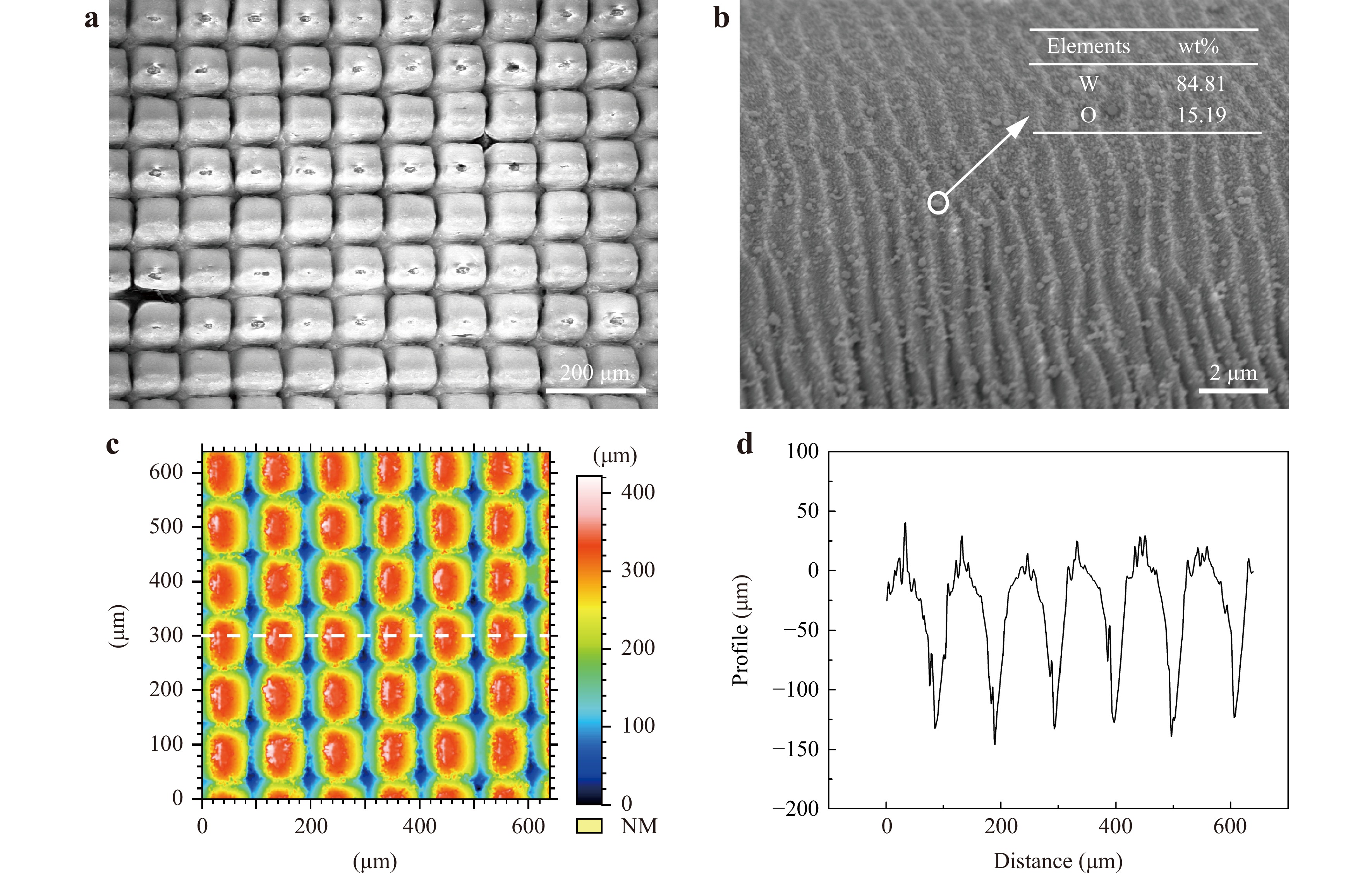
Fig. 1 Surface morphology of femtosecond laser textured W: SEM images of a W surface and b microgroove sidewall. c 3D morphology of W surface and d depth profile along the white line in c.
An SEM image and the elemental distribution at the joint of the W/Cu dual metal are shown in Fig. 2. A schematic of the melting, flow, and solidification of liquid Cu on the laser-textured W surface is shown in Fig. 3. During the SLM of Cu on the laser-textured W surface, the Cu powders were melted for laser irradiation; liquid Cu flowed into the microgrooves under the effect of gravity. In Fig. 3b, α is the microgroove angle, related to the d/w ratio, and θ is the intrinsic contact angle that liquid Cu makes with a flat solid wall. According to the Concus–Finn (CF) criterion23, spontaneous capillary flow occurs when θ > α. In this study, θ was increased by preparing the network texturing with deep microgrooves. The micro/nanostructures and the change in chemical composition on the sidewalls were beneficial for enhancing the wettability of liquid Cu on the W surface; thus, α decreased after laser texturing24. Therefore, liquid Cu spread easily in the microgrooves owing to the capillary effect, and high-quality mechanical interlocking formed at the interface when Cu filled the microgrooves. No apparent defects, such as pores or cracks, were observed (Fig. 2a). The W oxides had low bonding strength with the sidewall; therefore, they easily flowed into the melted Cu during SLM. In addition, the chemical activity of Cu is higher than that of W, with the substitution reactions of Cu and W oxides occurring at elevated temperatures. As shown in Fig. 2e, elemental O was detected in the microgrooves via EDS mapping. Fig. 2f shows the linear elemental distribution at the interface between W and Cu. Although the two metals have poor compatibility, an interdiffusion layer of approximately 710 nm in width was induced at the interface, possibly resulting from the comprehensive effects of the high temperature during the SLM of Cu and the femtosecond laser interaction on the W surface. In addition, the Cu content exhibited apparent fluctuations in the microgroove during the oxidation reaction.
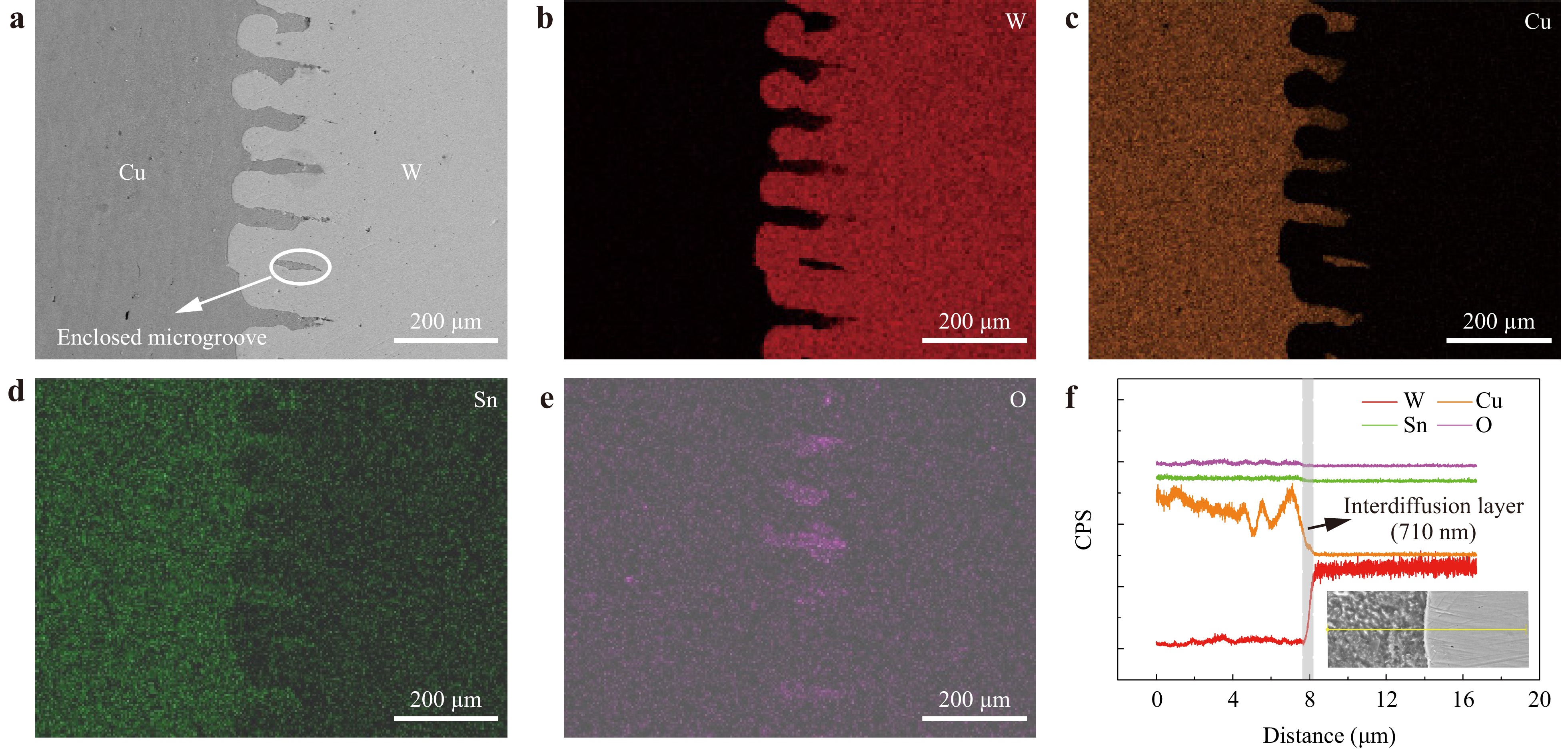
Fig. 2 a SEM image and EDS mapping (b W, c Cu, d Sn, e O) of W/Cu dual metal and f elemental distribution at the interface of W and Cu.
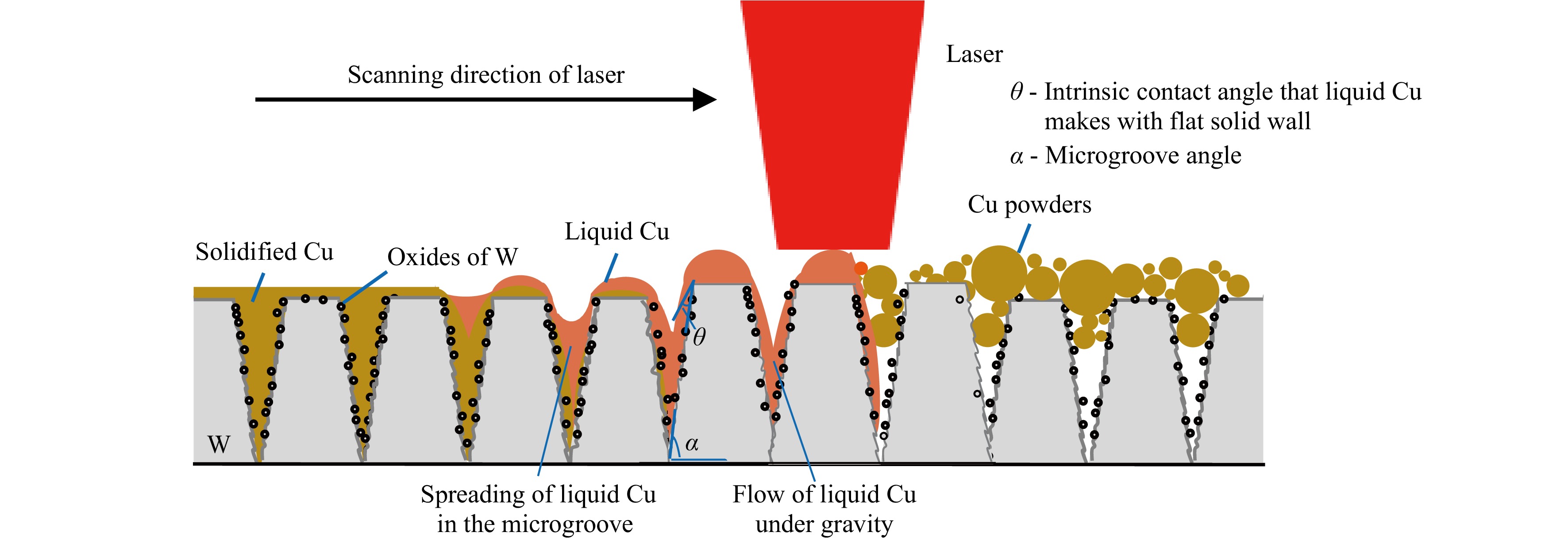
Fig. 3 Schematic of melting, flow, and solidification of liquid Cu on a laser-textured W surface.
According to the dimensions of the microgrooves shown in Fig. 3, the contact area at the interface increased by approximately 218% when mechanical interlocking was induced at the W/Cu interface. As shown in Fig. 4, the SLM-fabricated W/Cu dual metal fractured at the interface with a average bonding strength of ~123 MPa, close to that of the W/Cu dual metal obtained by diffusion welding3. The fracture morphology on the Cu side was examined to understand the fracture mechanism of the SLM-fabricated W/Cu dual metal. The fracture morphology was divided into two main categories: smooth and concave (Fig. 5a). In the smooth region, the main distributed elements were Cu and Sn (Fig. 5b−e). This region should be the contact region between the SLMed Cu and the untextured W surface. The fracture surface was blunt because no interdiffusion occurred at the interface and the bonding strength between W and Cu was low. The main elements distributed in the concave region are Cu, Sn, O, and W. W was in granular form and mainly distributed at the boundaries of the concave region. The concave region resulted from the fracture of the raised Cu in the W microgrooves. The fracture region is close to the microgrooves induced by the femtosecond laser beam. Therefore, O and W are detected in the concave region.
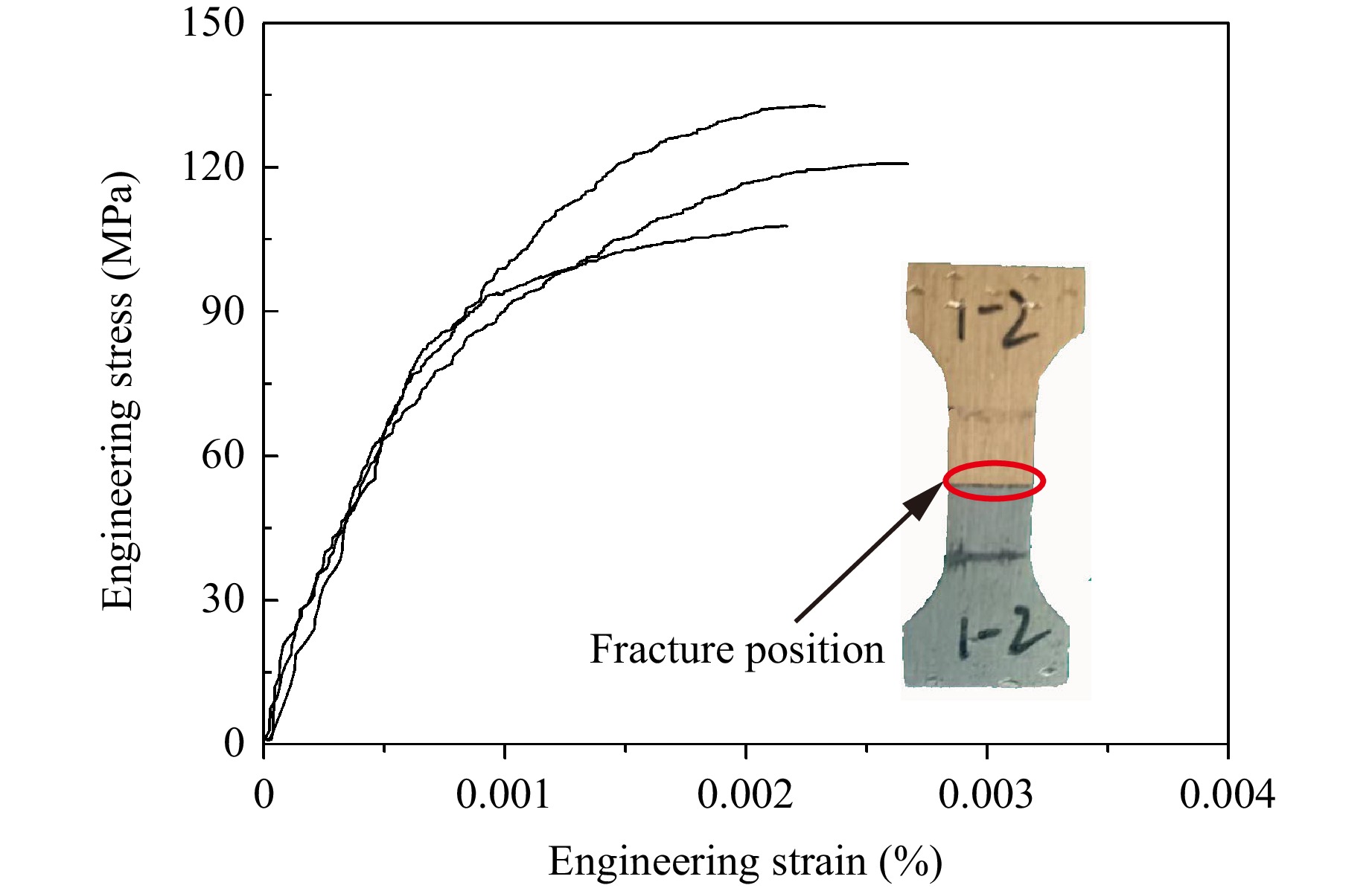
Fig. 4 Engineering strain–stress curves of SLM-fabricated W/Cu dual metal; inset: an image of a typical fractured sample.
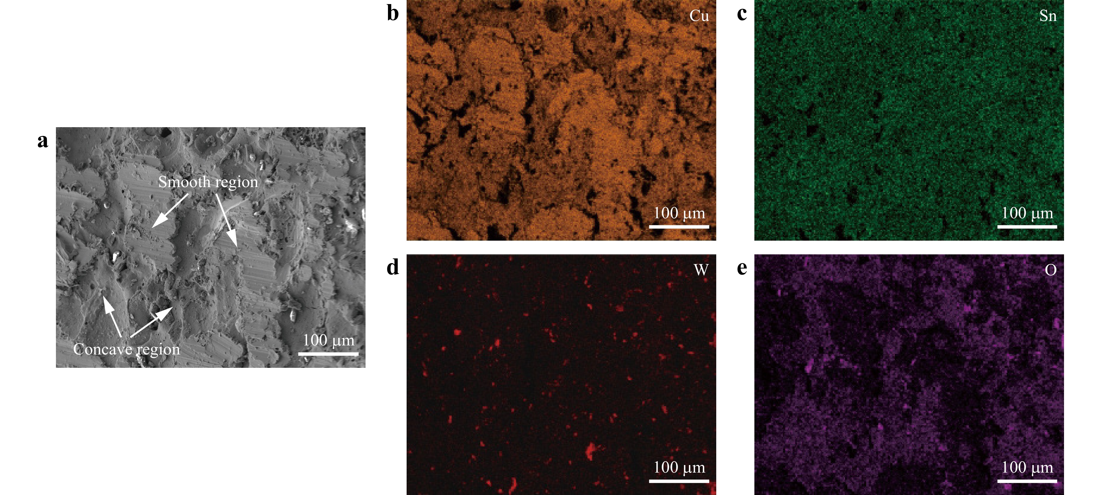
Fig. 5 Fracture morphology of W/Cu dual metal on the Cu side: a SEM image of fracture and b–e EDS mapping of Cu, Sn, W, and O.
A schematic of the fracture mechanism of the dual metal is shown in Fig. 6. When the W/Cu dual metal sample was tensile deformed, cracks were first induced on the SLMed Cu and the untextured region of the W surface owing to the small contact area in the tensile direction (Fig. 6b). In comparison, the selective laser melted Cu in the microgrooves was well bonded to W. With increasing tensile stress, crack growth occurred at the two inflection points of the raised Cu owing to the large stress concentration. The SLM Cu is a ductile crystalline metal; according to the maximum tangential stress criterion (MTS)25, the crack tends to grow from the tip in the direction along which the tangential stress reaches a critical value. The crack extension direction was consistent with the tangential stress direction and included an angle with the loading direction26,27 (Fig. 6c). The dimensions of the raised region were on the micrometer scale, and the cracks grew along two directions from the inflection points; circular-arc canyons formed on the Cu side when the cracks grew into the SLMed Cu (Fig. 6d). Overall, the contact interface of Cu and untextured W is the weak area of the joint; moreover, the topographic parameters of the microgroove also influence crack growth. To further enhance the joint strength, a subordinate structure can be designed on an untextured W surface; moreover, the topographic parameters of the microgroove should be optimized to decrease the stress concentration at certain positions.
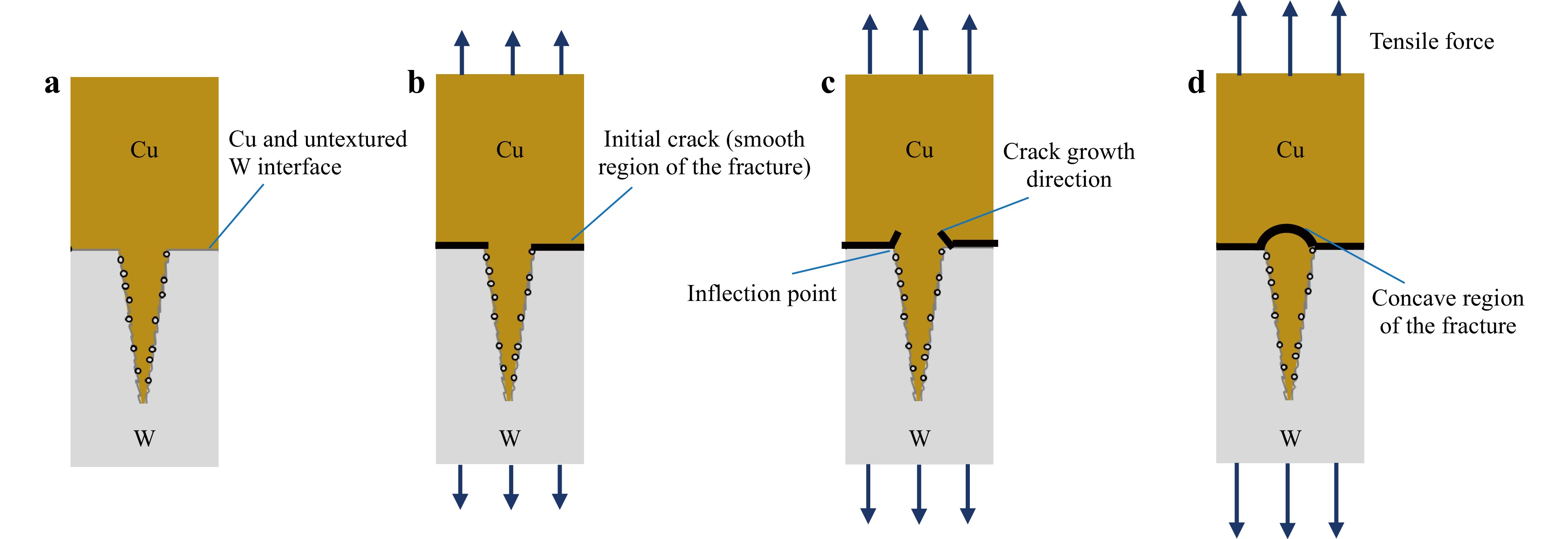
Fig. 6 Schematic diagram of fracture mechanics: a mechanical interlocking structure before tensile deformation, b crack formation at the Cu/untextured W interface, c crack growth at inflection points, and d fracture of the W/Cu dual metal.
-
This study proposed using a laser micro-structuring method to regulate the melting, spreading, and solidification of Cu during the SLM of Cu on the W surface to suppress interfacial defects during the SLM of the W/Cu dual metal. As a result, a high-quality interlocking joint of W/Cu dual metal was obtained without translation. The conclusions are as follows:
(1) Using femtosecond laser texturing technology, deep microgroove network texturing was performed on the W surface. The sidewalls of the microgrooves formed periodic nanoripples and nanoparticles owing to the interaction between the femtosecond laser and W.
(2) When Cu was SLMed onto a laser-textured W surface, the micro/nanostructures facilitated the uniform spread of liquid Cu, which led to mechanical interlocking and inhibited defects at the W/Cu interface.
(3) During tensile deformation, cracks initially formed at the Cu/untextured W surface for a smaller contact area in the tensile direction, and the cracks grew into the SLMed Cu before fracture. The ultimate tensile strength of the W/Cu dual metal was ~123 MPa.
-
This study focused on the interface properties of W/Cu dual metal, with commercial forged pure W (W content > 99.95 wt.%) used directly to simplify the experimental process; the dimensions of the W substrate were φ13 × 12 mm2. The CuSn10 alloy (Cu-9.8Sn, wt.%) was melted onto a W surface using SLM to fabricate a W/Cu dual metal. The CuSn10 alloy powders were prepared by atomization method and had a diameter range of 15–45 μm. The surface of W was mechanically polished with 180–1500 grit SiC papers before laser texturing. According to previous studies on the direct laser joining of metals and polymers15,28, the microgroove structure promotes the spreading of the melted material and increases the contact area at the joint. Therefore, a microgroove network texturing with a spacing of 100 μm was prepared on the W surface using a 40 W femtosecond laser at a wavelength of 1060 nm. The laser beam exhibited a Gaussian profile and was directed to the W surface using a galvanometric scanner with a telocentric f-theta lens. The femtosecond laser texturing process was performed in air at a laser power of 32 W, scanning speed of 1000 mm/s, repetitive frequency of 800 kHz, and scanning time of 750. The dimensions of the laser-textured region were 12 × 12 mm2.
The main parameters of the SLM equipment used in this study were a maximum power of 500 W, a building size of 280 × 280 × 300 mm3, and a spot size of 80 μm. The W sample was fixed to the substrate of the SLM apparatus using glue. During SLM of Cu, the laser power, scanning speed, layer thickness, and hatch spacing were set to 200 W, 350 mm/s, 30 μm, and 80 μm, respectively, with Ar used as the shielding gas. A 10 × 10 mm square region was built on the laser-textured W surface using a scanning strategy that included a 67° rotation between the layers towards the building direction. The building height of Cu was 12 mm. A schematic diagram of the preparation procedure and an image of the final fabricated W/Cu dual metal are shown in Fig. 1. For comparison, Cu was also melted onto an untextured W surface using SLM with the same parameters; however, serious warping occurred at the edge region, resulting in formation failure of the sample.
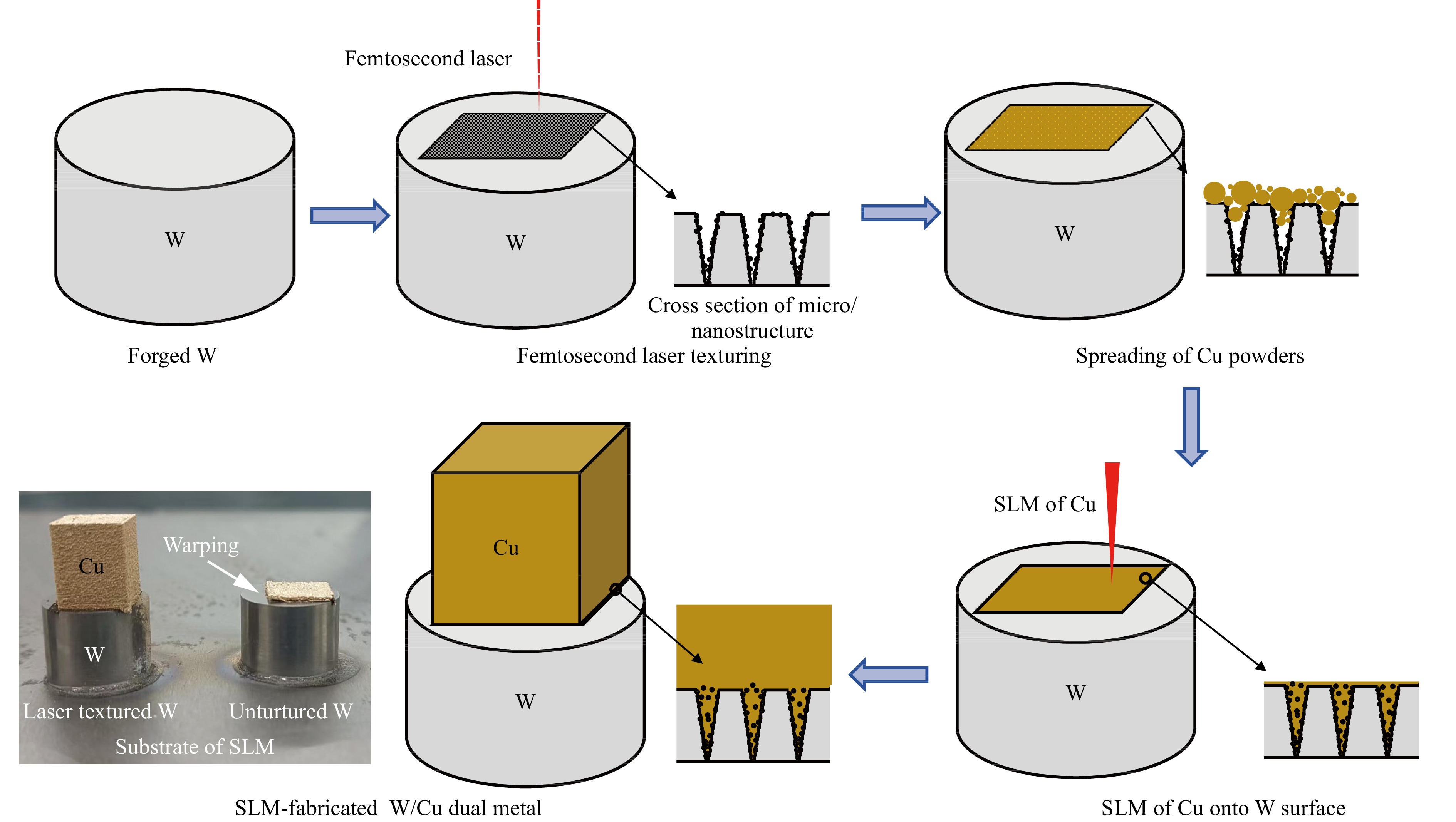
Fig. 7 Schematic of the preparation procedure and image of the final fabricated W/Cu dual metal.
The surface topography of the femtosecond-laser-textured W was characterized using a field-emission scanning electron microscope (FE-SEM, Zeiss Gimin 500) and a 3D laser scanning confocal microscope (LCSM, Zeiss LSM 900). To analyze the bonding quality between W and Cu, samples for microstructural characterization and tensile tests were prepared by wire electrical discharge machining perpendicular to the building direction. After mechanical polishing, an acidified ferric chloride solution was used to etch the W/Cu dual metals. An FE-SEM (Zeiss Gimin 500) equipped with an energy dispersive spectrometer (EDS, Ultim Max 65) was used to analyze the microstructure and compositional distribution at the interface. The tensile test specimens were 5 mm in width and 8 mm in gauge length. The tests were conducted using a universal testing machine at a crosshead speed of 0.1 mm/min, with the strain detected using a video extensometer (Shimadzu AG-Xplus). After tensile deformation, the fracture morphology of the dual metal was characterized using FE-SEM.
-
This work was financially supported by the Key Research and Development Program of the Anhui Province (202004b11020030).
Improving bonding strength of W/Cu dual metal interface through laser micro-structuring method
- Light: Advanced Manufacturing 5, Article number: (2024)
- Received: 19 January 2024
- Revised: 02 June 2024
- Accepted: 02 June 2024 Published online: 23 September 2024
doi: https://doi.org/10.37188/lam.2024.033
Abstract: Selective laser melting (SLM) is a promising technology for fabricating complex components with W/Cu dual metal. To enhance the interfacial bonding of W/Cu dual metal, we propose a novel approach using laser texturing to fabricate micro/nanostructures on the W surface. The micro/nanostructures promoted the spreading of Cu in the liquid, inhibited defects, and considerably increased the contact area between W and Cu by mechanical interlocking. To the best of our knowledge, a W/Cu dual metal was successfully prepared by SLM without a transition layer the first time. The bonding strength of the two materials reached 123 MPa, close to that of a W/Cu dual metal joint prepared by diffusion bonding.
Research Summary
Improving bonding strength of W/Cu dual metal interface through laser micro-structuring method
Selective laser melting (SLM) is a promising technology for fabricating complex components with W/Cu dual metal. To enhance the interfacial bonding of W/Cu dual metal, Prof. Ying-Chun Guan and her colleagues from Beihang University propose a novel approach using laser texturing technology to fabricate hybrid micro/nanostructures on the W surface. The micro/nanostructures promoted the spreading of Cu in the liquid, inhibited defects, and considerably increased the contact area between W and Cu by mechanical interlocking. A W/Cu dual metal was successfully prepared by SLM without a transition layer by the team. The bonding strength of the two materials reached 123 MPa, close to that of a W/Cu dual metal joint prepared by diffusion bonding.
Rights and permissions
Open Access This article is licensed under a Creative Commons Attribution 4.0 International License, which permits use, sharing, adaptation, distribution and reproduction in any medium or format, as long as you give appropriate credit to the original author(s) and the source, provide a link to the Creative Commons license, and indicate if changes were made. The images or other third party material in this article are included in the article′s Creative Commons license, unless indicated otherwise in a credit line to the material. If material is not included in the article′s Creative Commons license and your intended use is not permitted by statutory regulation or exceeds the permitted use, you will need to obtain permission directly from the copyright holder. To view a copy of this license, visit http://creativecommons.org/licenses/by/4.0/.

 DownLoad: