


-
Rapid ongoing development of smart city, vehicular communication, fifth-generation (5G) network, and internet-of-things (IoTs) requires new hardware technology that allows more efficient use of space, power, and communication bandwidth.1,2 One effective and economical solution is to embed additional data access points and signal interrogators into existing infrastructures by deploying optically transparent microwave antennas onto vehicles, building windows, solar panels, communication facilities, etc3–5. Similar to traditional microwave antennas which are typically opaque, optically transparent antennas (OTAs) possess the same functionalities and can efficiently collect, process, as well as transmit microwave signals. In addition, they are transparent in the visible and near-infrared (IR) regions, rendering them easy to integrate with diverse optoelectronic devices, such as solar cells, displays, photodetectors, and more. For various practical applications, the OTAs are highly desirable to be fabricated on flexible substrates and applied over curved surfaces, such as skin, clothes, optical fibres, and vehicle windows6.
Early exploration of OTAs utilises transparent conductive oxides, such as Indium Tin Oxide (ITO) and Fluorine doped Tin Oxide (FTO), which exhibit high optical transparency (e.g. an averaged transmittance of ~ 85% or higher in the visible range) and low electrical resistivity (e.g. a sheet resistance of ~ 30 Ω/sq)7–9. However, transparent conductive oxides are brittle; thus, susceptible to cracking when bent, which makes them unsuitable for flexible device applications10. Consequently, there have been intensive research efforts to develop flexible OTAs based on ITO-free materials over recent years. Currently, several alternative materials have been exploited, including conductive polymers11, carbon-based materials12,13, and metal meshes14. Conductive-polymer-based OTAs can be conveniently fabricated on flexible substrates by screen-printing or inkjet-printing15. However, they generally exhibit reduced efficiency compared to traditional devices using opaque metals owing to the low conductivity of the polymer. In addition, conductive-polymer-based OTAs typically display certain colours and lack sufficient environmental stability, further limiting their practical usage. Carbon-based materials, such as graphene, can provide good mechanical flexibility and decent optical transparency16,17. However, their relatively large sheet resistance may be a limiting factor for microwave antenna applications. Although metal meshes can provide low electrical resistivity by delicately controlling the ratio of opening areas over their surfaces, they generally suffer from sacrificed optical transmittance. In addition, they require relatively complex patterning processes, and their crisscross topology with patterned opaque materials might affect the antennas’ aesthetic appearance18–20. In contrast to the above candidates, thin metal films show great potential for flexible OTA applications owing to their low electrical resistance and decent optical transmittance. Moreover, large-area and defect-free metal films can be readily prepared on flexible substrates using various physical vapour deposition (PVD) methods, such as evaporation and sputtering21,22. However, thin-metal-film-based OTAs inevitably encounter a trade-off between antenna transparency in the visible (high-frequency) region and radiation performance in the microwave (low-frequency) region. Specifically, decreasing the thickness of the metal film can increase the visible transparency of the device. However, this reduces the electrical conductivity of the film and deteriorates the performance of the OTA in the microwave region.
Here, we demonstrate a novel thin-metal-film-based flexible OTA platform using a nano-engineered dielectric-metal-dielectric (DMD) composite structure, which effectively overcomes the aforementioned trade-off between the optical transmittance and radiation performance of the antenna. An ultra-thin (7 nm), smooth, and highly conductive (sheet resistance ~ 12.5 Ω/sq) copper-doped silver film is employed as the central metal layer, which simultaneously guarantees the antenna’s high optical transmittance and low electrical resistance. Moreover, two dielectric layers of judiciously selected constituent material and film thickness are utilised to sandwich the thin doped Ag layer, which further promotes the antenna’s neutral colour appearance and enhances its optical transmittance, leading to an unprecedently high averaged relative visible transmittance of 98.29%. Using the developed device architecture, we experimentally demonstrate several individual and arrayed OTAs of decent performance, including (i) flexible planar dipole antenna that operates at 2.5 GHz and exhibits omnidirectional radiation pattern with a realised gain of −0.67 dBi; (ii) unidirectional planar Yagi-Uda antenna with a realised gain of 4.6 dBi at 2.8 GHz; (iii) patch antenna working in the C-band (4−8 GHz) with broadside radiation properties and gain up to −1.3 dBi at 5.8 GHz; (iv) high-gain Fabry-Pérot (FP) cavity antenna with a realised gain of 13.6 dBi at 8.1 GHz. The demonstration of these antenna representatives serves to illustrate the capabilities of the optically transparent DMD composite structure in supporting a diverse range of antenna designs and radio-frequency (RF) applications. This study provides an insight for the development of compact, efficient, and flexible OTAs that can be employed in an array of applications, including 5G and vehicular communication systems, wearable electronics, self-powered devices, and the IoTs.
-
Candidate materials for thin-metal-film-based OTAs include Ag, Cu, and Au23. Among them, Ag stands out by its highest electrical conductivity at microwave frequencies and lowest optical loss in the visible regime24. However, Ag films deposited using common sputtering or evaporation techniques are characterized by less-than-ideal structural stability, as well as large surface roughness resulting from the intrinsic 3D (Volmer-Weber) growth mode of Ag atoms, which precludes the formation of continuous and defect-free Ag films of thickness below ~ 15 nm23. Increasing film thickness to the range of 15−25 nm mitigates the issue of dis-continuous film formation and rough surface morphology; thus, achieving good electrical conductivity for microwave antenna applications. However, the visible transparency of the antenna is inevitably sacrificed owing to the large reflection and absorption losses caused by the thick metal film.
We recently demonstrated a new approach to fabricate ultra-thin (down to 6 nm) and ultra-smooth (RMS surface roughness < 1 nm) Ag films by doping a small amount of the second metal (e.g., Al, Cu, Ni, Ti, or Cr) during Ag deposition25,26. In addition, we have employed doped Ag in several optoelectronic devices, including organic solar cells27, polymer light emitting diodes28, plasmonic waveguides29, hyperbolic metamaterials30, and electromagnetic shielding coatings31,32. By adding a proper amount of second metal during the Ag deposition, the intrinsic 3D growth mode of Ag atoms is largely suppressed; consequently, ultra-thin and high-quality Ag films can be obtained on various substrates. A detailed analysis is provided in Ref. 26 and 29. Here, by leveraging this novel material, we exploit its application in high-performance flexible OTAs based on a dielectric-metal-dielectric (DMD) composite structure on a polyethylene terephthalate (PET) plastic substrate (Fig. 1a, b). The central metal film in the DMD structure acts as a conductive medium, whose resistivity largely determines the performance of the OTA in the microwave region. For this purpose, we employ Cu-doped Ag as it exhibits the lowest optical loss and best electrical conductivity among different doped Ag films, as indicated in our previous study28. To implement flexible OTAs, we utilise a 7-nm-thick Cu-doped Ag film with a measured sheet resistance as low as 12.5 Ω/sq, sufficient for most high-efficiency microwave antenna applications. The deposited film exhibits a smooth and defect-free surface morphology (Fig. 1c), with an AFM-measured surface roughness value as low as 0.42 nm28. This significantly minimises electron scattering loss at the film surface and grain boundaries, leading to a high optical transmittance and low sheet resistance.
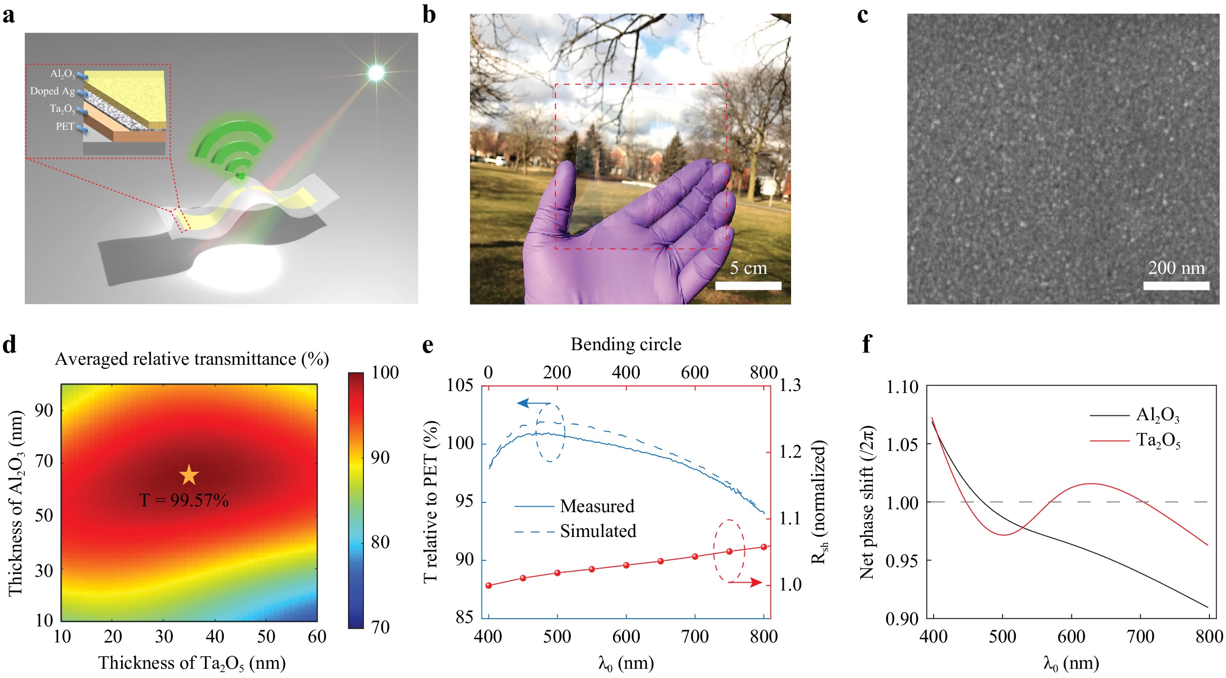
Fig. 1 a Schematic illustration of the proposed optically transparent antenna consisting of layers of Ta2O5, Cu-doped Ag, and Al2O3 on a flexible PET substrate. b Photo of a nanocomposite structure deposited on a PET substrate showing a close-to-unity relative visible transmittance. c Scanning electron microscope (SEM) image of a 7-nm-thick Cu-doped Ag film exhibiting a smooth surface morphology. d Calculated averaged visible (400−800 nm) transmittance of the Ta2O5 / Cu-doped Ag / Al2O3 nanocomposite structure, where transmittance through a bare PET substrate is used for reference. When the thicknesses of the Ta2O5 and Al2O3 layers are respectively set to 36 nm and 65 nm, the averaged relative transmittance reaches a peak value of 99.57%. e Left: Simulated (dashed blue curve) and measured (solid blue curve) relative transmission spectra of the nanocomposite structure. Right: Change in sheet resistance of the structure as a function of bending cycles (bending radius: 0.25 inch). The structure shows a ~6% increase in sheet resistance after 800 cycles of bending. f Calculated net phase shifts inside the Al2O3 layer (black curve) and Ta2O5 layer (red curve) as a function of free-space wavelength for the proposed nanocomposite structure made of 36-nm-thick Ta2O5 / 7-nm-thick Cu-doped Ag / 65-nm-thick Al2O3. A transmission resonance, which contributes to the structure’s enhanced visible transparency, occurs when the net phase shift equals multiples of 2π radians.
To further enhance the visible transmittance and colour neutrality of the antenna, we sandwich the thin Cu-doped Ag layer between two dielectric films. The employed dielectric layers help match the impedance of the surrounding media; thus, significantly suppressing reflection from the DMD structure. In addition, they act as protective layers that prevent environmental damage to the thin Ag film and guarantee the operational stability of the antenna. To maximise the antireflection effect, a dielectric material with a high refractive index in the visible (Ta2O533 in this case) is employed for the layer on the substrate side, and a material with a lower refractive index (Al2O3 in this case) is used for the layer on the air side. The associated layer thicknesses are judiciously chosen to achieve maximum visible transmittance and neutral colour appearance simultaneously. When the film thicknesses of the Ta2O5 and Al2O3 layers are 36 nm and 65 nm, respectively, corresponding to a total structural thickness of 108 nm, the calculated visible transmittance through the DMD structure reaches a peak value (Fig. 1d). For the wavelength of interest in this study (400−800 nm), the structure exhibits a high and flat transmission spectrum (Fig. 1e, dash line). When compared with a bare PET substrate, the average transmittance is as high as 99.57%, reaching a near-unity visible transparency. Transmission through a 7-nm-thick Cu-doped Ag film on a PET substrate is plotted in Figure S1, Section I of the Supporting Information. To further evaluate the colour appearance of the structure, the calculated transmission spectrum is converted into coordinates in the L*a*b* colour space, as defined by the International Commission on Illumination. The L* value is calculated to be 98.99, indicating high optical transparency. The a* and b* values are calculated to be −0.70 and 0.41, respectively, indicating a neutral colour appearance.
The enhanced optical transparency of the nanocomposite can be attributed to the broadband transmission resonances induced by the two dielectric layers. To reveal this effect, the net phase accumulation inside each dielectric layer, $ \varphi $, is calculated. The phase accumulation includes both the reflection phase shifts at the two interfaces and the propagation phase through the dielectric layer. A transmission resonance, which contributes to the enhanced optical transmittance, occurs when the aforementioned net phase accumulation equals multiples of 2π radians. As shown in Fig. 1f, a single transmission resonance inside the Al2O3 layer is located at free-space wavelength $ {\mathrm{\lambda }}_{0} $ = 474 nm, and several transmission resonances inside the Ta2O5 layer are located at $ {\mathrm{\lambda }}_{0} $ = 449, 572, and 707 nm, respectively. Owing to the low reflectance at both the top and bottom interfaces of each dielectric layer, the transmission resonances are weakly confined inside the cavity; thus, exhibit broad spectral bandwidths. Consequently, they overlap in the spectral domain, leading to a high and flat transmission spectrum of the nanocomposite.
The nano-engineered composite-based flexible microwave antennas are fabricated by sequentially sputtering Ta2O5, Cu-doped Ag, and Al2O3 layers onto plastic substrates. The thicknesses and refractive indices of the deposited films are characterised using spectroscopic ellipsometry (see Experimental Section for details). The measured transmission spectrum of the sample is plotted in Fig. 1e (solid line), which corresponds well to the simulated curve and exhibits an averaged relative transmittance of 98.94 ± 0.24%. The associated L*a*b* values are calculated to be 98.61 ± 0.09, −0.50 ± 0.01, and 0.22 ± 0.03, respectively, which also agree well with numerically predicted values. The cited uncertainties represent one standard deviation from the measured data. In addition, the structure demonstrates exceptional mechanical flexibility, as shown in Fig. 1e, where the sheet resistance (Rsh) remains nearly unchanged after 800 bending cycles (bending radius: 0.25 inch). These characterization results confirm the superiority of our nanocomposite over existing transparent conductor materials for both flexible and rigid OTA applications in terms of electrical conductivity and optical transparency. A comparison of the critical parameters of different candidate materials is listed in Table 1. Notably, most of these candidate materials exhibit optical transmittance levels below or around 80%, limiting their suitability for applications requiring high optical transparency. Conversely, materials with higher transmittance typically compromise the electrical conductivity, potentially affecting the antenna gain and efficiency. Thus, simultaneously achieving high transparency and conductivity is challenging. However, our proposed nanocomposite structure exhibits exceptional performance, achieving a record-high transmittance level of up to 98.3% across a broad wavelength spectrum, while maintaining a comparatively low sheet resistance. This combination of properties renders it an ideal candidate for OTA applications.
Ref. Material Sheet Resistance (Ω/sq) Measured Optical Transmittance Wavelength Range 34 Conductive polymer 0.08 62.5% (a. T.) @ 550 nm 20 ITO 15 72% (a. T.) 380 – 750 nm 20 Metal mesh 0.048 69.8% (a. T.) 380 – 750 nm 19 Metal mesh 0.5 70% (a. T.) 400 – 700 nm 35 Metal mesh 0.18 62.1% (a. T.) 400 – 800 nm 35 Multilayer film 2.52 68.63% (a. T.) 400 – 800 nm 36 Graphene 18 85% (a. T.) 350 – 900 nm 37 Three-layer stacked graphene 80 90.4% (a. T.) @ 550 nm 38 FTO/ITO 4 75% (a. T.) 400 – 800 nm 39 AgNW 8.5 85% (a. T.) @ 550 nm 40 Ag/Ti 0.017 59.2% (a. T.) 400 – 800 nm 40 ITO/Ag/ITO 5.05 71.3% (a. T.) 400 – 800 nm This work Ta2O5/Cu-doped Ag/Al2O3 12.5 89.7% (a. T.) 400 – 800 nm 91.4% (a. T.) @ 550 nm 98.3% (r. T.) 400 – 800 nm (Notes: ‘a.T’ means absolute transmittance, and ‘r.T’ means relative transmittance over that of the substrate) Table 1. Comparison of the key parameters of different candidate materials for OTA applications
We utilise the obtained highly transparent and flexible nanocomposites to implement several OTAs of representative microwave-shaping functionalities, which respectively operate within the fourth-generation long-term-evolution (4G-LTE) band (e.g. 1.7 GHz and 1.9 GHz band), Bluetooth band (2.4 GHz), and Wi-Fi channels (2.4 GHz and 5.9 GHz bands). The first OTA is a half-wave dipole antenna commonly used as a TV or broadcasting antenna in wireless communication networks41,42. A schematic illustration of the implemented flexible dipole antenna is shown in Fig. 2a, where the alternating currents on its two dipole arms oscillate in phase to generate omnidirectional RF radiation. The resonant frequency of the dipole antenna can be tuned by adjusting its arm length. Three devices (D2.0, D2.5, and D4.2) with resonant frequencies of 2.0 GHz, 2.5 GHz, and 4.2 GHz are implemented. The antennas have the same arm width (w = 13 mm) and separation gap (g = 3 mm), and their arm lengths (L) are respectively chosen as 25.0 mm (D2.0), 17.5 mm (D2.5), and 8.0 mm (D4.2). The measured reflection spectra (return loss, S11) are shown in Fig. 2b, where the resonant frequencies correspond well with simulated ones (Fig. 2b)43. The three antennas exhibit operating bandwidths of 0.82 ± 0.02 GHz (D2.0), 0.77 ± 0.04 GHz (D2.5), and 0.91 ± 0.04 GHz (D4.2), respectively, with return losses exceeding 10 dB. Typically, the measured antenna properties may exhibit slight disparities compared to the simulated properties. This primarily stems from the idealised conditions underpinning the simulation, falling short of fully considering complex real-world scenarios, such as multipath propagation, cable and connecter losses, and fabrication imperfections. In our case, the disparities between the simulation and measurement results, although present, remain relatively modest and well within the acceptable margins. The simulation continues to demonstrate commendable accuracy in predicting the experimental measurements. In addition, the experimentally measured resonant frequencies match well with the numerical calculations based on empirical equations (Fig. 2c). The details of the calculation process are presented in Section II of the Supporting Information. The red solid lines in Fig. 2d plot the characterised radiation patterns of the D2.5 OTA on the E- and H-planes, showing a maximal realised gain of −0.67 ± 0.22 dBi. Its radiation performance is similar to that of dipole antennas made of opaque materials, such as Ag ink (denoted by blue lines in Fig. 2d) and Cu paste (denoted by black lines in Fig. 2d), and comparable to the reported state-of-the-art transparent dipole antennas16,17,20. Moreover, our OTAs provide a close-to-unity relative visible transmittance, which is considerably greater than previously reported results. Similar findings are observed for the nanocomposite-based OTAs operating at 2.0 GHz and 4.2 GHz (Section III, Supporting Information). Owing to the extremely thin nanocomposite structure, we characterise OTA mounted on a flexible polydimethylsiloxane (PDMS) substrate. The experimental findings demonstrate the remarkable flexibility and foldability of the OTA (Fig. 2e, f). Notably, the resonant frequency and −10 dB bandwidth exhibit only minor fluctuations across a range of bending angles (−70° < $ \theta $ < 70°). Note that these slight variations have negligible impact on the antenna’s performance for practical applications, as the antenna consistently maintains S11 below −10 dB in close proximity to its operating frequency (~3 GHz). The flexible OTA also demonstrates robust performance after cyclic bending (Section IV, Supporting Information). However, such results may not be easily achieved with other transparent (e.g. ITO) or opaque (e.g. silver ink and copper) antennas owing to their relatively rigid surfaces and thick conductive coatings.
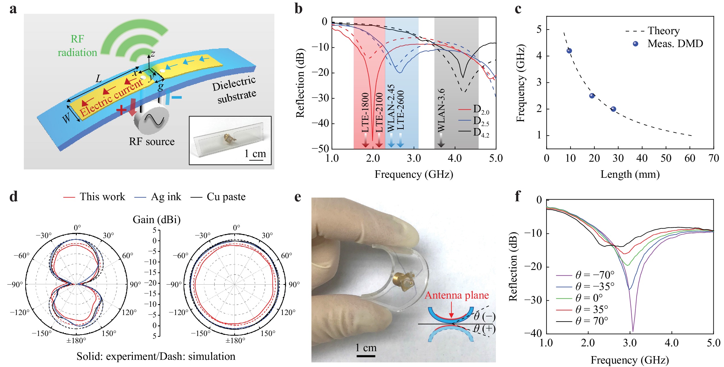
Fig. 2 a Schematic illustration of a flexible transparent dipole antenna made of the proposed nanocomposite. The inset shows a photo of a 2.0 GHz dipole antenna mounted on rigid acrylic substrate. The red and blue arrows represent the two polarities of the electric current. b Measured (solid curve) and simulated (dashed curve) reflection spectra of three transparent dipole antennas designed for operation in the 4G/5G wireless communication band, which include several commonly used bands such as LTE-1800, LTE-2100, and WLAN-2.45. c Measured resonant frequencies of the nanocomposite-based dipole antennas with different arm lengths, which show close correspondence to the theoretical curve. d Measured realised gain as a function of observation angle (radiation pattern) on the E (x-z) plane (left panel) and H (y-z) plane (right panel) for three 2.5 GHz dipole antennas, whose arms are respectively made of the proposed nanocomposite (red lines), silver ink (blue lines), and copper paste (black lines). e Photograph of a hand-bent transparent dipole antenna mounted on a polydimethylsiloxane (PDMS) substrate, showing its excellent flexibility. f Measured reflection spectra of the antenna at different bending angles.
We demonstrate a high-gain Yagi-Uda OTA with unidirectional radiation properties for shortwave communication and broadcasting applications44,45. The Yagi-Uda OTA is designed to resonate at a centre frequency of 2.5 GHz, and all its driven and parasitic elements (reflectors and directors) are made of the nano-engineered composite (Fig. 3a, b). The details of the geometric parameters of the antenna are elaborated in Section V of the Supporting Information. Microwave emission is first sourced from the driving element (i.e. a half-wave dipole operating at 2.5 GHz), and the reflector and other parasitic elements re-radiate waves to form constructive (destructive) interference in the forward (backward) direction, creating a unidirectional radiation pattern. Fig. 3c displays the reflection spectrum of a fabricated Yagi-Uda OTA, where the simulated and measured results correspond well with each other43, showing a 0.87 ± 0.05 GHz bandwidth centered at 2.5 GHz. The calculated and measured radiation patterns (Fig. 3d, e) are in good agreement with each other, showing unidirectional radiation with a front-to-back ratio of 6.2 ± 0.33 dB and a maximum measured gain of 2.9 ± 0.32 dBi at 2.5 GHz. The cited uncertainties represent one standard deviation from the measured data. Compared to the omnidirectional dipole in Fig. 2, the Yagi-Uda OTA exhibits a higher directivity and larger gain within its operational band (Fig. 3f) owing to constructive interference in the forward propagating direction. The realised gain can be further improved by increasing the number of transparent directors or using a double-layer antenna configuration46,47.
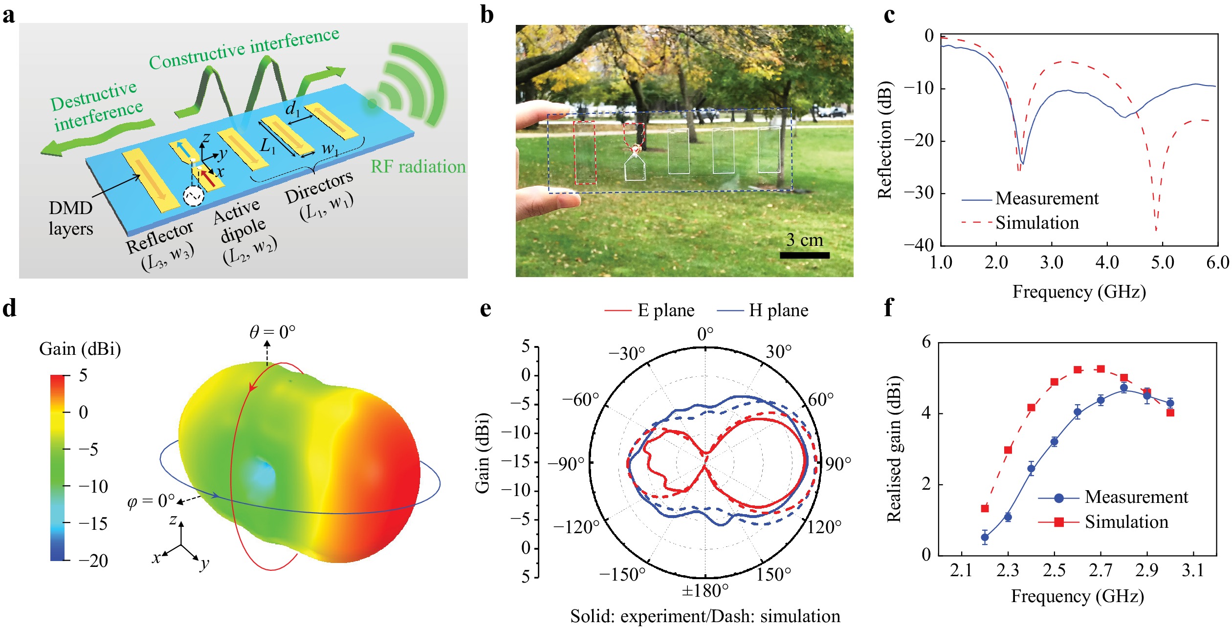
Fig. 3 a Schematic illustration of the high-gain Yagi-Uda OTA with unidirectional radiation property. b Photo of a fabricated sample. c Measured and simulated reflection spectra of the Yagi-Uda OTA. d Calculated three-dimensional (3D) radiation pattern of the Yagi-Uda OTA operating at 2.5 GHz. e Measured two-dimensional (2D) radiation patterns of the Yagi-Uda OTA operating at 2.5 GHz. The measured and simulated results are represented by solid and dashed lines, respectively. f Measured and simulated realised gain as a function of operating frequency for the Yagi-Uda OTA.
Next, we demonstrate a group of low-profile, transparent microstrip patch antennas that operate in the C-band (4−8 GHz) and X-band (8−12 GHz), covering the WLAN-5.8 and satellite communication frequencies48,49. A microstrip patch antenna is similar to an open cavity with magnetic walls, where the fringing electric fields at the edges are equivalent to magnetic currents that oscillate in phase to generate broadside radiation (Fig. 4a). Fig. 4b shows a photograph (top view) of the fabricated transparent patch antenna, which resonates at 5.8 GHz and is fed by a coaxial cable. Fig. 4c plots the reflection spectra of three patch antennas (P5.8, P6.5, and P8.2) with different patch dimensions, which respectively resonate at 5.8 GHz, 6.5 GHz, and 8.2 GHz (throughout the C-band and X-band). Details of the antenna dimensions are provided in Section VI of the Supporting Information. The measured resonant frequencies correspond well with the analytically calculated frequencies (Fig. 4d; details of the analytical calculation are discussed in Section VII, Supporting Information). Fig. 4e displays the measured E-plane (left) and H-plane (right) radiation pattern of the patch antenna P5.8 with a realised gain of −1.3 ± 0.16 dBi, indicating that the device functions well in the C- and X-band. As shown in Fig. 4e, the realised gain and radiation efficiency of the OTAs may be lower than those constructed from commonly used metals (e.g. Ag and Cu) and substrate materials (e.g. FR-4 and Rogers). This deficiency arises from additional losses in both the conductive and substrate materials. However, it is imperative to emphasise that despite the marginally reduced efficiency, our OTAs offer unparalleled transparency and high flexibility, which are unattainable for traditional antennas relying on printed circuit board technology.
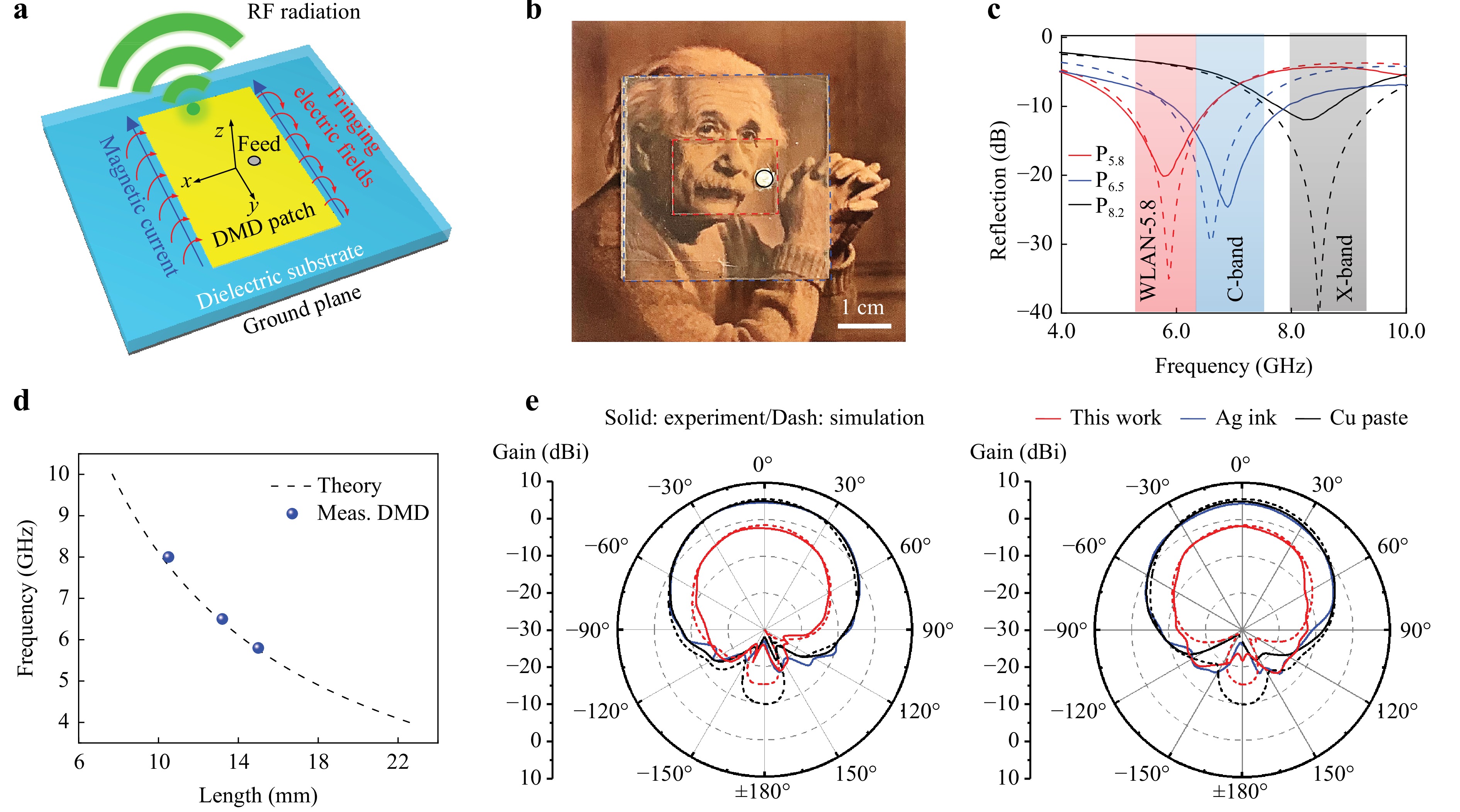
Fig. 4 a Schematic illustration of the low-profile, transparent microstrip patch antenna. b Photo of a fabricated sample. c Measured (solid line) and simulated (dashed line) reflection spectra of three different transparent patch antennas, P5.8, P6.5, and P8.2, with operating frequencies respectively centered at 5.8 GHz, 6.5 GHz, and 8.2 GHz. d Measured resonant frequencies of patch antennas with different patch lengths, which show close correspondence to the theoretical curve. e Measured E-plane (left panel) and H-plane (right panel) radiation patterns of the 5.8 GHz patch antennas, which are respectively made of the proposed nanocomposite (red lines), silver ink (blue lines), and copper paste (black lines).
Finally, we implement a highly directional Fabry-Pérot (FP) cavity antenna50,51, designed to resonate at 8.2 GHz (Fig. 5a). The antenna’s key part is a “visible-region-transparent” and “microwave-region-reflective” metasurface made of the proposed nanocomposite. The metasurface, acting as a partially reflective surface (PRS) for the FP cavity antenna, is formed using subwavelength nanocomposite square patches arrayed over the PET surface. Based on the ray-tracing method, multiple reflections occurring between the partially reflective metasurface and the ground plane of the antenna can form a highly directive beam at the broadside. Fig. 5b shows a photograph of the fabricated antenna, where its constituent PRS metasurface is separated from the copper ground plane by a suitable distance h = 19 mm. The ground plane is covered with a paper painting of “The Great Wave off Kanagawa”. The FP cavity of the antenna is excited using a small patch antenna located underneath the ground plane. The transparent metasurface acts as a protective layer for the painting and simultaneously reshapes and focuses the radiation from the patch antenna source. Fig. 5c shows the simulated and measured reflection spectra of the FP cavity antenna (with the metasurface) and the source patch antenna (without the metasurface). It can be observed that the FP cavity antenna exhibits a resonant frequency of 8.1 GHz, similar to that of its source patch antenna. The simulated and measured radiation performances of this FP cavity antenna, which correspond well, are shown in Fig. 5d, e, respectively. The device exhibits a realised gain of up to 13.6 ± 0.33 dBi, and good co- and cross-polarisation isolation levels up to 22 ± 0.64 dB at the centre frequency. Compared to its source patch antenna (with a realised gain of 6.5 ± 0.24 dBi), the realised gain of the FP antenna with the transparent metasurface is remarkably enhanced (Fig. 5f). This high realised gain can benefit various long-distance shortwave communication and sensing applications.
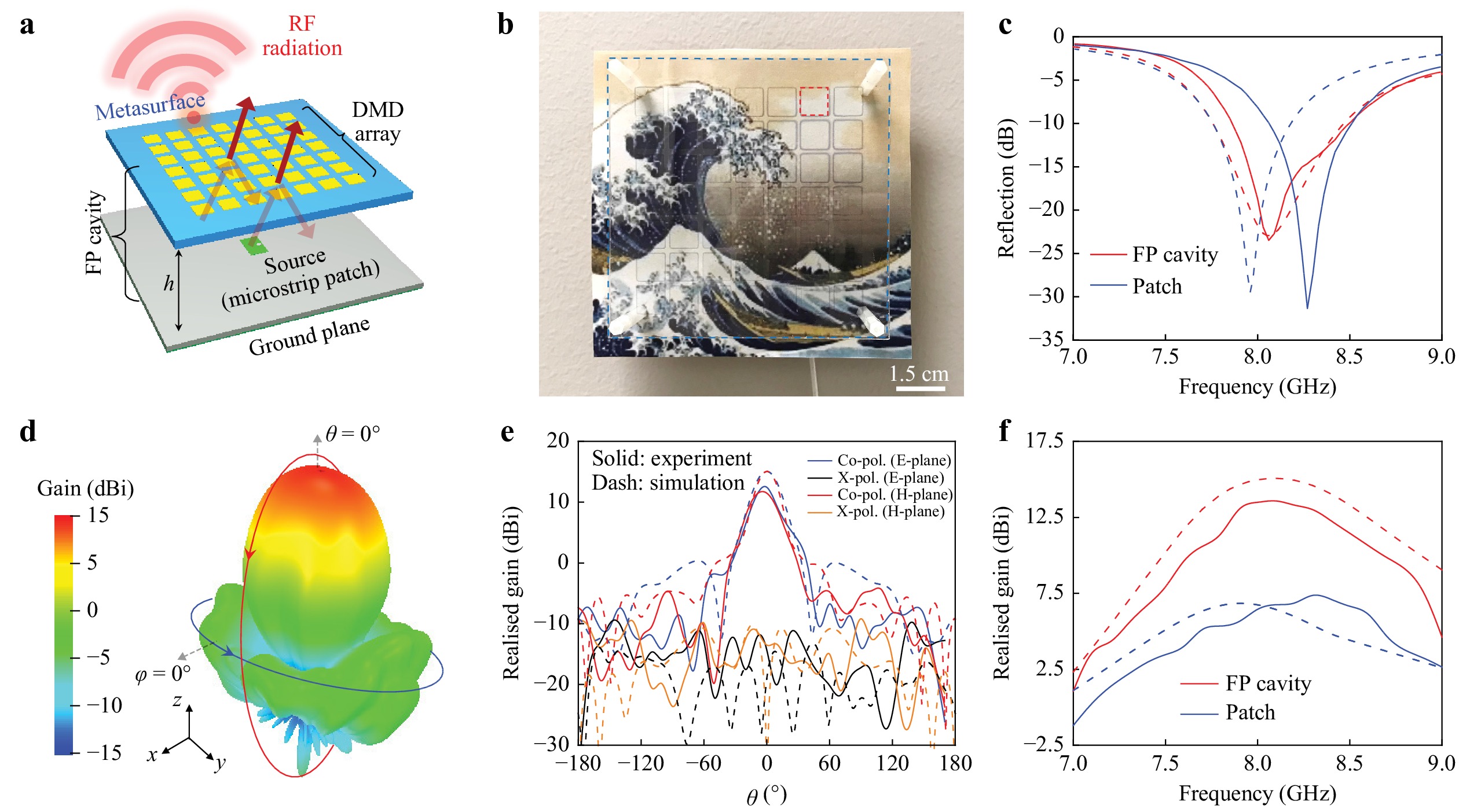
Fig. 5 a Schematic illustration of the Fabry-Pérot cavity antenna, consisting of a transparent metasurface separated from the ground plane by a distance of h. A small microstrip patch antenna located underneath the ground plane acts as the feeding source of the cavity antenna. b Photo of a fabricated sample. The antenna’s ground plane is covered with a paper painting of “The Great Wave off Kanagawa”. c Reflection spectra for the Fabry-Pérot cavity antenna and the patch-antenna source. The solid and dashed lines represent the measured and simulated results, respectively. d−e Calculated and measured radiation patterns for the antenna operating at 8.2 GHz. Here, the E and H planes correspond to the x-z and y-z planes, respectively. The measured cross-polarization patterns are also displayed here to show the good co- and cross-polarization isolation level of this antenna. f Realised gain against frequency response for the Fabry-Pérot cavity antenna and its patch source, where the Fabry-Pérot cavity antenna shows an obviously enhanced gain.
Recently, there has been a growing interest in building multifunctional IoT nodes, which seamlessly integrate optical devices and microwave antennas for high-efficiency information transmitting and broadcasting in wireless sensor networks. In this regard, the Fabry-Pérot cavity antenna with a transparent metasurface PRS allows easy vertical integration of various optical devices with microwave-radiating apertures; thus, facilitating a practical and cost-effective realisation of compact monolithically integrated IoT nodes. Additionally, the transparent metasurface, with strategic design and integrated control devices (e.g. diodes), may be extended to programmable metasurfaces that hold the potential for dynamic electromagnetic wave manipulation52,53. In particular, the suggested OTAs, distinguished by their exceptional optical transmittance and radiation efficiency, offer promise for a diverse range of applications beyond the capabilities of conventional opaque antennas and existing OTAs. For example, these OTAs can be integrated into automobile windshields to facilitate satellite communication and into eyeglasses for IoT applications. Furthermore, their ultra-thin and flexible nature allows integration onto curved surfaces, such as human skin and clothes, underscoring their potential for wearable applications.
-
In this study, we develop a highly transparent and conductive nanocomposite structure comprising Ta2O5 / Cu-doped Ag / Al2O3 thin layers that can be easily fabricated on flexible substrates using simple and low-cost physical vapour deposition methods. This nanocomposite structure, when used to build microwave OTAs, outperforms traditional constituent materials, including metal meshes and organic polymers, owing to its broadband optical transmittance, low sheet resistance, and excellent mechanical flexibility. The fabricated structure exhibits an averaged visible transmittance as high as 98.29% compared to a bare plastic substrate, and simultaneously, a sheet resistance as low as 12.5 Ω/sq. We demonstrate different types of omnidirectional (dipole) and unidirectional (Yagi-Uda and patch) antennas with operating frequencies covering the S, C, and X bands (1.5−12 GHz), which accommodate most WiFi, Bluetooth, WLAN 5.8, 4G/4G-LTE, and short-range 5G communication applications. Moreover, we implement an optically transparent metasurface, which is employed as the radiating facet of a microwave Fabry-Pérot antenna to achieve a realised gain of up to 13.6 dBi. The demonstrated transparent and flexible nanocomposite structure offers a viable solution for building compact and multifunctional intelligent systems that breaks the lateral design limitation faced by opaque devices and allows vertical integration of “invisible” RF and microwave components with diverse optical devices. Our findings have widespread applications in wearable wireless electronics, IoTs, smart cities, vehicular communications, and next-generation wireless communication infrastructures.
-
Device fabrication: Layers of Ta2O5, Cu-doped Ag, and Al2O3 were sequentially sputter-deposited onto flexible PET substrates. The Ta2O5 film was deposited using a Ta2O5 target through a reactive radio-frequency (RF) sputtering process with an oxygen flow rate of 2 standard cubic centimetres per minute (sccm). The calibrated deposition rate was 0.303 nm/s. The Cu-doped Ag film was deposited by co-sputtering Cu and Ag. The concentrations of Cu and Ag were controlled by adjusting the sputtering powers of the Cu and Ag targets. The calibrated deposition rates of Ag and Cu were 1.109 and 0.019 nm/s, respectively. The Al2O3 film was deposited using an Al2O3 target via RF sputtering at a calibrated rate of 0.053 nm/s. The obtained nanocomposite structure was then cut by a laser cutter (with a cutting resolution of ~ 25 μm) to produce the antenna geometries.
Material characterization: The refractive indices and film thicknesses of the deposited layers were characterised by spectroscopic ellipsometry using the interference enhancement method30,54. The associated measurement details are presented in Section VIII of the Supporting Information. The optical transmittance was measured using a spectroscopic ellipsometer operating in the transmission mode. The sheet resistance was measured using a four-point probe. The surface morphology of the Cu-doped Ag film was characterised by scanning electron microscopy and atomic force microscopy.
Antenna characterization: Simulations of the antenna properties were conducted using the ANSYS High Frequency Simulation Software (HFSS). Reflection coefficient measurements were performed using a vector network analyser (VNA) that was pre-calibrated in the frequency range of 1−10 GHz. The radiation properties of the antennas were measured inside an anechoic chamber room with the undertest antenna mounted on a controlling machine that could rotate over a range of 360° to capture the entire radiation pattern of the antennas. The transmitted signal was generated using a signal generator with a fixed input power of 20 dBm. A broadband horn antenna with a realised gain of 13 dBi at 2.6 GHz was used as the transmitter antenna. Our undertest antenna was placed 2.5 m away from the transmitter, and the received power was recorded using a spectrum analyser. Finally, the radiation pattern was calculated using the Friis equation.
-
C.Z. would like to thank Ms. Moxin Li for her assistance in editing the figures.
Functional plastic films: nano-engineered composite based flexible microwave antennas with near-unity relative visible transmittance
- Cheng Zhang1, *, ,
- Liang Zhu2,
- Chengang Ji3,
- Zhilu Ye2,
- Nabeel Alsaab2,
- Minye Yang2,
- Yuhui Hu1,
-
Pai-Yen Chen2, *, ,
 ,
, -
L. Jay Guo3, *, ,
- Light: Advanced Manufacturing 5, Article number: (2024)
- Received: 29 June 2023
- Revised: 16 June 2024
- Accepted: 17 June 2024 Published online: 30 June 2024
doi: https://doi.org/10.37188/lam.2024.036
Abstract: Microwave antennas are essential elements for various applications, such as telecommunication, radar, sensing, and wireless power transport. These antennas are conventionally manufactured on rigid substrates using opaque materials, such as metal strips, metallic tapes, or epoxy pastes; thus, prohibiting their use in flexible and wearable devices, and simultaneously limiting their integration into existing optoelectronic systems. Here, we demonstrate that mechanically flexible and optically transparent microwave antennas with high operational efficiencies can be readily fabricated using composite nanolayers deposited on common plastic substrates. The composite nanolayer structure consists of an ultra-thin copper-doped silver film sandwiched between two dielectric films of tantalum pentoxide and aluminum oxide. The material and thickness of each constituent layer are judiciously selected such that the whole structure exhibits an experimentally measured averaged visible transmittance as high as 98.94% compared to a bare plastic substrate, and simultaneously, a sheet resistance as low as 12.5 Ω/sq. Four representative types of microwave antennas are implemented: an omnidirectional dipole antenna, unidirectional Yagi-Uda antenna, low-profile patch antenna, and Fabry-Pérot cavity antenna. These devices exhibit great mechanical flexibility with bending angle over 70°, high gain of up to 13.6 dBi, and large radiation efficiency of up to 84.5%. The proposed nano-engineered composites can be easily prepared over large areas on various types of substrates and simultaneously overcome the limitations of poor mechanical flexibility, low electrical conductivity, and reduced optical transparency usually faced by other constituent materials for flexible transparent microwave antennas. The demonstrated flexible microwave antennas have various applications ranging from fifth-generation and vehicular communication systems to bio-signal monitors and wearable electronics.
Research Summary
Ultrathin silver-based nanocomposite enables the future of optically transparent antennas
Optically transparent antennas (OTAs) are poised to revolutionize a multitude of applications including smart cities, vehicular communication, and the Internet of Things. Despite their potential, the performance of OTAs has been constrained by the inherent trade-off between optical transmittance and radiation efficiency. Addressing this challenge, a collaborative team from China and the USA has developed flexible, high-performance OTAs utilizing an innovative ultrathin silver-based dielectric-metal-dielectric nanocomposite structure. This advanced structure achieves an experimentally verified average visible transmittance of 98.94% relative to a bare plastic substrate, accompanied by a low sheet resistance of 12.5 Ω/sq. The team implement four OTA variants: omnidirectional dipole, unidirectional Yagi-Uda, low-profile patch, and Fabry-Pérot cavity antennas. These antennas exhibit impressive flexibility, enduring bending angles exceeding 70°, and demonstrate remarkable performance with gains reaching 13.6 dBi and radiation efficiencies up to 84.5%.
Rights and permissions
Open Access This article is licensed under a Creative Commons Attribution 4.0 International License, which permits use, sharing, adaptation, distribution and reproduction in any medium or format, as long as you give appropriate credit to the original author(s) and the source, provide a link to the Creative Commons license, and indicate if changes were made. The images or other third party material in this article are included in the article′s Creative Commons license, unless indicated otherwise in a credit line to the material. If material is not included in the article′s Creative Commons license and your intended use is not permitted by statutory regulation or exceeds the permitted use, you will need to obtain permission directly from the copyright holder. To view a copy of this license, visit http://creativecommons.org/licenses/by/4.0/.

 DownLoad: