


-
High-performance X-ray imaging techniques depend on high-quality bulk crystals that can fully attenuate high-energy X-rays and effectively convert photon energy into readable electronic signals through direct or indirect processes1,2. Most typical X-ray responsive materials, including Si, a-Se, CdTe, CsI, and GOS, are produced through high-temperature crystallization processes, which increase the barrier to low-cost and high-performance X-ray detectors, especially for single crystals as direct semiconductors. Consequently, bulk scintillator crystals have dominated the X-ray detection market over the past several decades.
Although there are strict requirements for high-performance scintillators, a new wave of research has emerged since solution-processable halide perovskite materials were developed in 20093, promoting advancements in optoelectronics, including solar cells, light-emitting diodes, and X-ray detectors4,5. Perovskites have shown success as both direct semiconductors and indirect scintillators for high-performance X-ray imaging, dosimetry, and CT imaging6,7. Perovskite materials with diverse compositions can be assembled at various scales such as colloidal quantum dots (CQDs), polycrystalline films, 2D superlattices, and large-dimensional single crystals, using low-cost solution processes8. The corresponding X-ray sensitivity is already several orders of magnitude higher than that of a typical amorphous selenium devices while maintaining a valuable high signal-to-noise ratio. Consequently, the dosage for X-ray or CT imaging can be dramatically reduced to avoid irradiation damage to the human body, fostering the prosperity and development of the field9-12. According to the Web of Science database, publications on perovskite X-ray detectors have been steadily increasing since 2013, with over 300 papers anticipated on this topic in 2025.
Owing to innovations in solution-processed material design, X-ray detection technology is undergoing unprecedented advancements. Writing in Light: Science & Applications, Song et al. design a large, environmentally friendly ZnO CQD scintillator13. A meter-scale film, with a thickness on the order of hundreds of micrometres, exhibited visible transparency exceeding 96% and a large Stokes shift owing to bright singlet/triplet hybrid self-trapping excitons (STEs). The negligible self-absorption and bright triplet excitons yield elevated photon yields, enabling real-time X-ray imaging at a high resolution of 42 lp/mm and low dose rate of 38 nGy/s over a large area of 5000 cm2. The response speed of microseconds is also excellent for most applications. It is important to note that the transparency and Stokes shift of scintillators are paramount, because medical scintillators must possess a significant thickness (several millimetres or even centimetres) to completely attenuate the penetrated X-rays. The output light yield at such a thickness may be impaired, and the spatial resolution may decrease owing to the isotropic characteristics of light. ZnO is always recognised as comprising atoms with low atomic numbers, and its smaller attenuation coefficients require a greater thickness than the dominant commercial counterparts to absorb the same energy X-rays, as illustrated in Fig. 1, which poses one of the main challenges for commercial scintillators. Therefore, controlling the degree of aggregation and assembly morphology is crucial for ZnO CQD scintillators, and surface chemistry should play an important role.
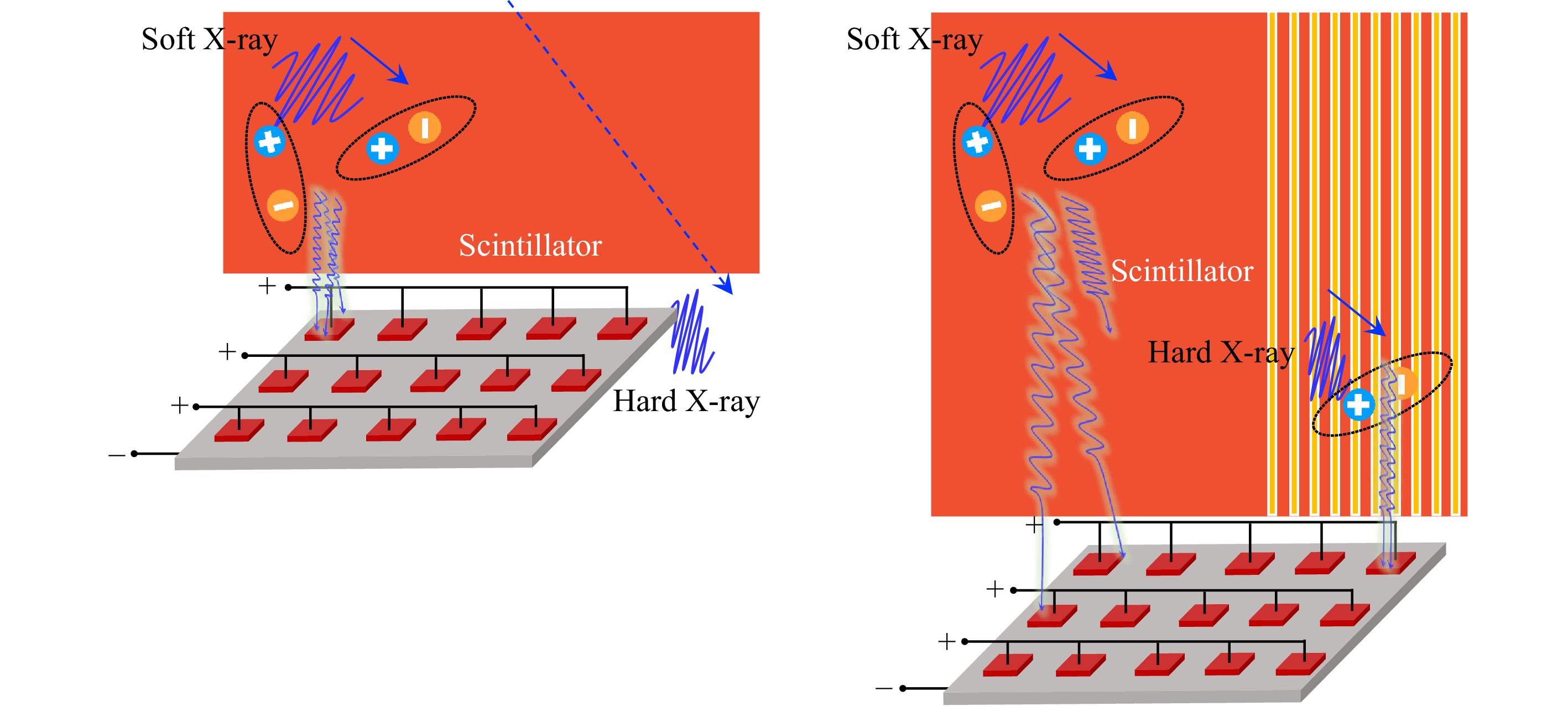
Fig. 1 Schematic demonstrating shows the challenge of high-performance scintillators. Although a thin scintillator can alleviate the self-absorption and light scattering effect, it can not fully use the energy of penetrating X-rays due to the limited stopping power. A thick scintillator may suffer limited output light yield and reduced X-ray imaging spatial resolution, while confined light total reflection fibre design can solve the light scattering problem.
The ZnO CQD scintillator is appealing because it is environmentally friendly nature, involves low-cost solution processes, and exhibits high performance, especially if thick samples designed for 120 to 160 keV hard X-ray imaging are further demonstrated. The detection quantum efficiency allows for a fair comparison with commercial sensors. Pixelized structures can be deployed on large-area scintillators to maximise the output light yield. This study will pave the way for the production of new medical X-ray detectors for routine examination scans.
Solution-processed material innovation is sparking a research boom on X-ray imaging techniques
-
Haotong Wei*, ,

- Light: Advanced Manufacturing , Article number: (2025)
- Received: 30 March 2024
- Revised: 17 April 2025
- Accepted: 22 April 2025 Published online: 04 August 2025
doi: https://doi.org/10.37188/lam.2025.036
Abstract: X-ray-responsive materials are often expensive and limited because of the monopolistic and complex high-temperature crystallisation technology required. Solution-processed material innovation offers a low-cost and vast design space for a new generation of X-ray detectors aimed at for high X-ray imaging performance.
Rights and permissions
Open Access This article is licensed under a Creative Commons Attribution 4.0 International License, which permits use, sharing, adaptation, distribution and reproduction in any medium or format, as long as you give appropriate credit to the original author(s) and the source, provide a link to the Creative Commons license, and indicate if changes were made. The images or other third party material in this article are included in the article′s Creative Commons license, unless indicated otherwise in a credit line to the material. If material is not included in the article′s Creative Commons license and your intended use is not permitted by statutory regulation or exceeds the permitted use, you will need to obtain permission directly from the copyright holder. To view a copy of this license, visit http://creativecommons.org/licenses/by/4.0/.

 DownLoad: