


-
The wafer-scale fabrication of high-quality two-dimensional (2D) van der Waals materials (vdWMs) with direct bandgap photoluminescence (PL) has enabled the use of atomically thin semiconductors in foldable displays and quantum photonics applications1,2. However, their intrinsically low quantum yields pose a critical bottleneck for practical applications3; thus, extensive efforts have been expended to improve their PL quantum yield4–7. Precisely shaping metallic architectures to adapt to the local dielectric environment and trigger localised surface plasmon resonances (LSPRs) can amplify the local electromagnetic field and accelerate radiative recombination via the Purcell effect, thus improving the PL intensity by up to four orders of magnitude5.
Despite significant progress, two challenges remain for LSPR systems: spatial confinement and Ohmic losses8. First, the electromagnetic field is tightly confined to nanoscale hotspots, thus restricting Purcell-enhanced PL to isolated subwavelength regions. Second, strong field localisation on metallic protrusions induces unavoidable Ohmic losses, thereby resulting in severe parasitic absorption that diminishes the overall efficiency and offsets the benefits of accelerated radiative decay rates.
As illustrated in Fig. 1, Yeonjeong Koo et al. demonstrated a 32-fold enhancement in 2D PL across an 800 μm2 area by exploiting surface lattice resonance (SLR) in a vdWM-Au slot lattice hybrid platform9. SLR emerges from the coupling of LSPRs with counterpropagating surface plasmon polaritons, thus forming a 2D standing wave that uniformly distributes enhanced electromagnetic fields uniformly across the lattice10. Unlike the broad linewidths of LSPRs (> 200 meV), SLRs exhibit a much narrower resonance linewidth (~65 meV) owing to reduced radiative losses and coherent interactions within the periodic lattices. Moreover, by confining the field within dielectric gaps instead of on metallic surfaces, SLR structures effectively mitigate Ohmic losses and exciton quenching, which are typically encountered at metal-semiconductor interfaces in LSPR systems.
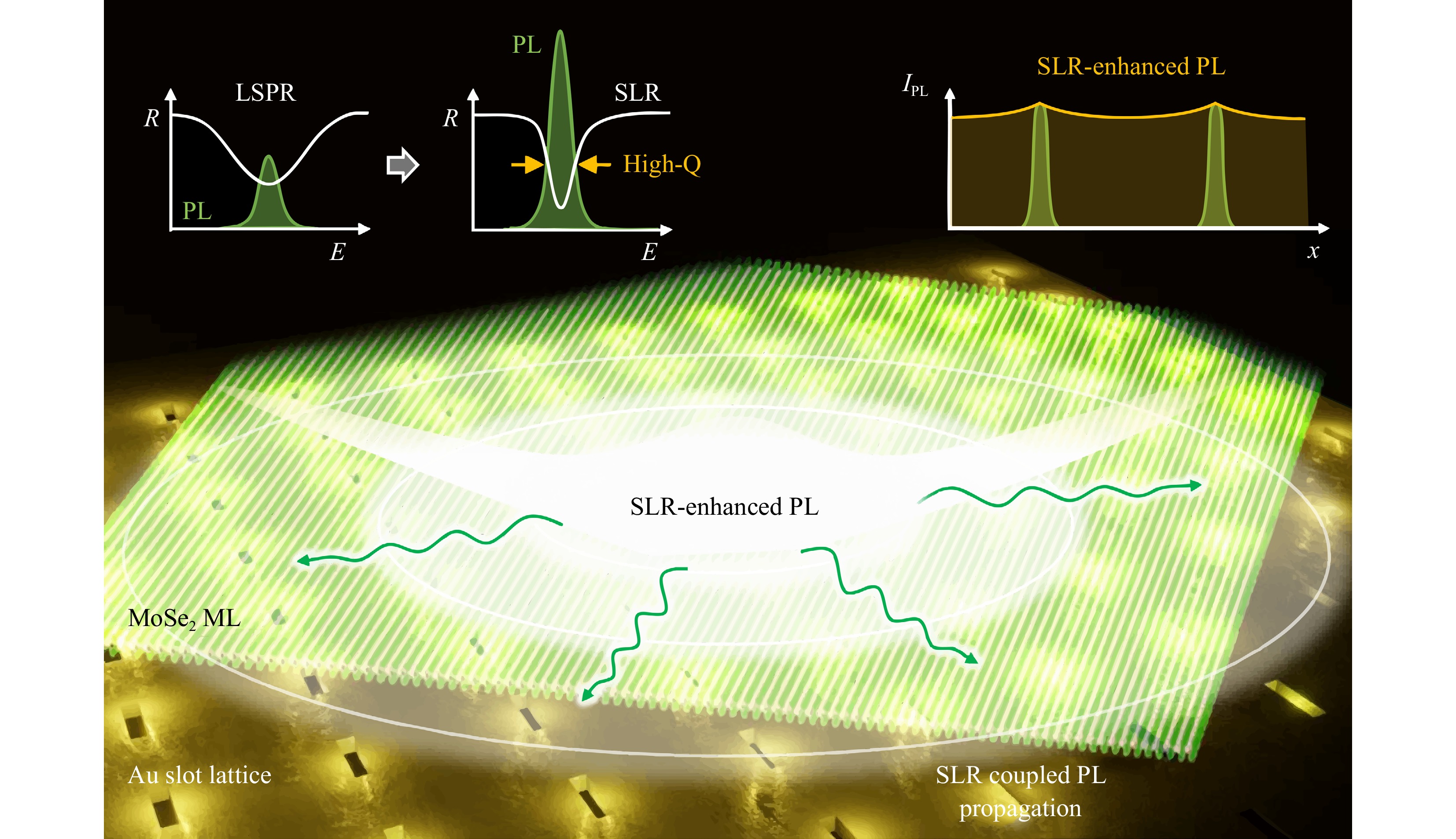
Fig. 1 Schematic illustration of SLR-enhanced PL and its propagation in vdWMs-Au slot lattice hybrid platform. Figure reproduced and modified from Ref 9.
Angle-resolved spectroscopy revealed clear indications of strong coupling between surface plasmons and Rayleigh anomalies, thus resulting in coherent surface plasmon polaritons on the Au surface, which is characteristic of the pronounced SLR effect11. Whereas conventional 2D photoluminescence radiates isotropically and decays within submicron distances (< 550 nm), SLR-coupled emission exhibits high in-plane momentum and directional propagation over macroscopic distances of up to 16 μm9. Although excitons can flow over a long distance12, this extended PL enhancement is independent of the emitter size and instead arises from collective plasmonic coupling and engineered momentum matching intrinsic to the periodic lattice.
The SLR hybrid platform, although simple in structure, offers significant advantages. SLR delivers wafer-scale PL enhancements that overcome the low quantum yield of vdWMs and the spatial confines of conventional LSPRs. Such precise engineering of the local dielectric environment affords unprecedented control over light–matter coupling and spontaneous emission dynamics. Simultaneously, it bridges nanoscale plasmonic design with macroscale device integration, which is promising for wafer-sized 2D optoelectronic components3. Nevertheless, a tradeoff exists between strong Purcell enhancement and large-area scalability10. Although LSPRs offer intense localised fields and SLRs enable spatial coherence, their distinct physical mechanisms render simultaneous optimisation challenging. This spatial-intensity paradox, compounded by material losses and structural constraints, warrants innovative hybrid designs that balance between confinement and coherence.
The demonstrated synergy between SLRs and 2D semiconductors creates avenues for realising advanced photonic designs that facilitate dynamically tunable, large-area, atomically thin light-emitting devices. First, integrating van der Waals heterostructures with tunable band alignments may enable the dynamic control of enhanced PL emission. Furthermore, anisotropic plasmonic lattices may allow polarisation- or chirality-selective light routing, which is essential for quantum photonic circuits. Additionally, combining SLRs with topological photonic platforms, such as the observed bound states in the continuum of SLRs13, can result in ultrahigh-quality hybrid modes and reconfigurable light sources at the nanoscale.
Surface lattice resonance promotes high-momentum, large-area 2D emission enhancement
- Light: Advanced Manufacturing , Article number: (2025)
- Received: 14 May 2025
- Revised: 11 June 2025
- Accepted: 18 June 2025 Published online: 29 July 2025
doi: https://doi.org/10.37188/lam.2025.052
Abstract: Recent progress in harnessing surface lattice resonance within a van der Waals material–Au slot lattice hybrid platform has enabled a 32-fold enhancement in two-dimensional photoluminescence over an 800 μm2-area, which is promising for realising scalable atomically thin light-emitting devices.
Rights and permissions
Open Access This article is licensed under a Creative Commons Attribution 4.0 International License, which permits use, sharing, adaptation, distribution and reproduction in any medium or format, as long as you give appropriate credit to the original author(s) and the source, provide a link to the Creative Commons license, and indicate if changes were made. The images or other third party material in this article are included in the article′s Creative Commons license, unless indicated otherwise in a credit line to the material. If material is not included in the article′s Creative Commons license and your intended use is not permitted by statutory regulation or exceeds the permitted use, you will need to obtain permission directly from the copyright holder. To view a copy of this license, visit http://creativecommons.org/licenses/by/4.0/.

 DownLoad: