


-
Silicon carbide (SiC), as a third-generation semiconductor material, is widely used in high-performance applications such as high-voltage, high-temperature, and high-frequency electronic devices mainly owing to its high critical-breakdown electric field and appreciable carrier mobility1–3. In order to meet the needs of these advanced applications, large SiC crystal ingots must be sliced into thin wafers, which serve as substrates for device fabrication. Traditional cutting methods, such as wire sawing, use diamond wires to slice large crystal ingots4,5. While this method offers relatively high cutting efficiency, it presents several challenges. The kerf loss, constrained by the width of the diamond wire, often exceeds 150µm per wafer6,7. Additionally, crystal defects and surface damage induced during the slicing process contribute to material loss in subsequent grinding, leading to significant wastage of crystal material during slicing and thinning8.
Laser-assisted slicing is a non-contact, wear-free, and dry slicing technique that holds significant promise in the semiconductor wafer slicing industry. This technique involves focusing a laser to a fixed depth inside the crystal, where laser energy deposition induces internal modification and crack formation9. The wafer can be separated along the modification-crack layer using mechanical stretching10,11, cold split12 or photo-electrochemical etching13. By controlling the local interaction process and the laser-induced modification, it is possible to effectively minimize the sacrificial layer, reducing material loss associated the slicing process. Femtosecond laser, with its high peak energy, can induce multiphoton ionization inside wide-bandgap semiconductor materials, enabling precise internal modification or ablation of the material14,15. Karki et al. conducted a series of experiments, which demonstrated that four-photon absorption dominates in silicon carbide under femtosecond laser excitation16. Compared to traditional long-pulse lasers, femtosecond lasers offer the advantage of reducing the thermal effect of the process. This can reduce the size of the heat affected zone and heat-induced mechanical stress and thus minimize material damage near the modification area17,18. Li et al. innovatively employed spiral-trajectory femtosecond laser focusing technology to achieve monolithic fabrication of high-precision three-dimensional light-absorbing helical micro/nanostructures within transparent media19. Therefore, the use of femtosecond laser is a preferential choice for high-precision laser-assisted slicing.
Despite these important advantages, there are several challenges associated with using femtosecond lasers for SiC slicing. One major issue is the occurrence of strong nonlinear effects during the propagation of the femtosecond pulses in semiconductor materials20–22. Prior to the focus, intense laser pulses efficiently ionize these materials, creating a pre-focal plasma that tend to absorb, shield or deflect the light. This can prevent the achievable laser energy density at the focal point. Additionally, the high nonlinear index of the materials makes it prone to self-focusing, that causes a further degradation of the energy deposition and a subsequent increase of the thickness of the material modification layer23,24. These nonlinear effects can undermine the effectiveness of the laser-assisted slicing process if not properly controlled.
Several important works investigated the influence of temporal parameters for SiC slicing. Kim et al. employed methods such as splitting a single pulse into a double-pulse sequence where the pulses are separated by a picosecond time delay to achieve a modification layer with a thickness of 25 µm. This enables slicing of the SiC wafer with thin modification thickness25,26. However, this approach results in limited crack propagation, leading to the need of short intervals (25 μm) between adjacent laser scanning lines, which reduces the efficiency of large-area scanning. Zhang et al. extended the pulse duration to induce internal modification and crack formation. However experiments shows that significant self-focusing effects persist using conventional picosecond lasers leading to considerable defect formation below the crack layer and a subsequent excessive material loss27. With these two methods, important limitations remain in laser energy deposition inside materials. Recently, ultrafast trains of femtosecond laser pulses have been used to achieve efficient energy deposition inside materials like silicon (Si) and gallium arsenide (GaAs)28,29. With an increase of the number of sub-pulses at terahertz repetition rate, these works show that it is possible to effectively diminish the pre-focal plasma shielding effects. This burst-mode of irradiation facilitates the writing of high-precision internal structures in Si and GaAs in comparison to irradiations with single intense pulses. Although SiC was not specifically addressed in these studies, the similarity in material responses to ultrafast pulse trains suggests that such approaches could enhance the performance of slicing technologies applicable to SiC.
In this paper, we investigate this methodology to control laser energy deposition and evaluate the benefits for laser-assisted slicing of SiC ingots into individual wafers. The control parameters of the ultrafast pulse train (including the total energy and the number of sub-pulses within the train) are demonstrated to precisely modulate carrier excitation distributions near the laser focus. This capability enables the creation of highly localized extreme conditions within the material, facilitating precise modifications and controlled crack initiation. With parameters optimization, we achieve single-layer modifications and cracking (thickness of 16.5 μm) within semi-insulating SiC crystals. We demonstrate the potential of the method for low-material-loss slicing of SiC into wafers.
-
In our experiment, we used a 500 fs femtosecond laser with a central wavelength of 1030 nm. The pulse repetition rate was set to 1 kHz, and the laser energy was adjusted by using a half-wave plate and a polarizing beam splitter. To generate the pulse trains, we employed a custom arrangement of birefringent crystals to split the incoming laser pulses into multiple components and temporally shape the irradiation profile, as illustrated in Fig. 1. Calcite crystals were cut and polished along the optical axis plane. When a linearly polarized pulse enters a crystal perpendicularly to the polished surface, it is split into two pulses with polarizations which are parallel to the fast and slow axes of the crystal. The time delay between these two pulses is calculated as follows:
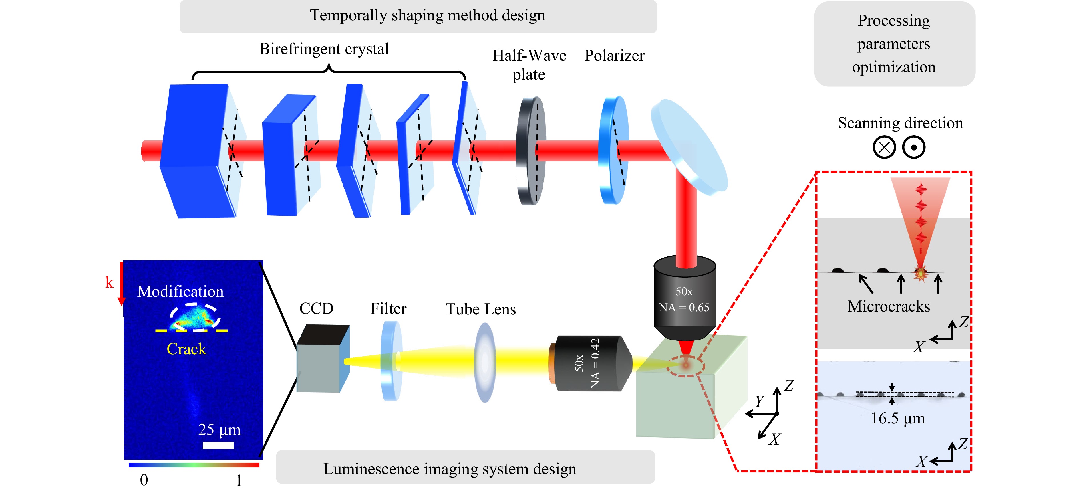
Fig. 1 Illustrations including the birefringent crystal configuration for generating ultrafast trains of pulses and luminescence microscopy system.
$$ \Delta t=x\left(\frac{1}{{v}_{o}}-\frac{1}{{v}_{e}}\right) $$ where $ x $ is the crystal thickness, $ {v}_{o} $ is the group velocity along the ordinary axis, and $ {v}_{e} $ is the group velocity along the extraordinary axis.
Birefringent crystals were stacked as shown in Fig. 1. The fast axis of the first crystal was rotated 45° relative to the laser’s linear polarization direction, and each subsequent crystal is rotated 45° relative to the previous one, arranged from thickest to thinnest. The thickness of the crystal is half of the one in the front and the last one is 0.8 mm thick. After passing through n crystals, the initial pulse is shaped into a train of 2n sub-pulses. The time delay between sub-pulses in the produced train is 0.47 ps. Each sub-pulse is linearly polarized, and the polarization directions of the two adjacent sub-pulses are perpendicular to each other. A half-wave plate and polarizer were placed after the crystals to project all sub-pulse polarizations in the same direction. The half-wave plate’s fast axis was set to 0° or 22.5° relative to the horizontal direction, depending on the number of stacked crystals (odd or even). The polarizer was set to 0° to the horizontal direction, ensuring all sub-pulses have the same polarization and energy. The laser beam then focused inside semi-insulating silicon carbide crystals using an objective lens equipped with a correction collar for spherical aberration compensation (Olympus LCPLN50XIR, NA 0.65). The laser was incident parallel to the $ \left[0001\right] $ direction and focused at a specific depth, then scanned along the $ [11\bar{2}0] $ direction. The SiC $ (1\bar{1}00) $ plane has larger interplanar spacing and less silicon and carbon atoms, which makes it easier to modify SiC material along $ [11\bar{2}0] $ orientation30. After scanning the entire surface, the wafer was adhered to stainless steel plates and tensile force was applied to separate the wafer.
During laser processing, we used an side-imaging system to capture luminescence emitted from the laser-induced plasma within the crystal, indicating energy deposition. This imaging system includes a long-working-distance objective (Mitutoyo MPLANAPONIR, NA 0.42), a tube lens, a short-pass filter (cutoff wavelength 750 nm), and a CCD camera. The system collects carrier bandgap recombination luminescence induced by nonlinear absorption in the silicon carbide crystal. Since undoped silicon carbide is an indirect bandgap semiconductor, carrier recombination involves phonon-assisted transitions, resulting in weak luminescence. Therefore, we increased the camera’s exposure time to observe the internal luminescence signal. To ensure comparability of luminescence signals under different laser parameters, we normalized the brightness values of luminescence images by dividing by the exposure time while keeping the CCD camera gain constant.
-
For these experiments, we used a 500-micron-thick semi-insulating 4H-SiC sample. We raised the sample surface 100 μm above the laser focal plane. The desired thickness of the peeled wafer is between 100 μm and 350 μm. Due to the effect of spherical aberration, the actual laser focusing point will be located at a depth greater than the height of the focus shift relative to the sample surface. Silicon carbide has a refractive index of 2.6 at 1030 nm. Based on the formula for focus movement31, the theoretical value of the actual focus was estimated to be about 290 μm below the crystal surface. Then we adjusted the objective’s correction ring to achieve optimal correction at this depth. The correction ring setting was chosen based on the luminescence imaging of the laser beam focus within the crystal at different positions (see supplementary information Fig. S1). We first studied the effects of different total pulse energies and sub-pulse numbers on single-line scanning irradiation within the silicon carbide. The scanning speed was set at 650 μm/s for these investigations.
Fig. 2a shows top views of single-line structures under various laser parameters. The zones of the laser-induced modifications are well contrasted and appear darker because of highly absorbing defective SiC. In contrary, the areas of the laser-induced microcracks appear brighter because of an increase of reflectivity, which is attributed to the reflection of the incident light27,32. We note that a low number of applied sub-pulses and a modest total energy of the pulse train, such as 2.5 μJ total energy with 2 or 4 sub-pulses, fail to achieve internal modification and crack propagation in SiC. At the opposite, increasing the total energy to 20 μJ is systematically causing surface ablation. When the number of sub-pulses is increased to 16 or more, a stable continuous modification line is observed even with total energy as low as 2.5 μJ. This indicates that increasing number of sub-pulses for a given total energy increases energy deposition and enhances the success rate for stable internal modification by the laser. When the number of sub-pulses is greater than or equal to 8, with the increase in total energy, a noticeable bright white region appears around the modified area, which is the crack propagation zone. The extreme conditions achieved near focus causes an internal micro explosion of the material, leading to excessive local stress in the crystal, which in turn induce the micro-cracks. The enlarged image on the right shows more detailed morphology of the internal modification, surface ablation, and cracks.
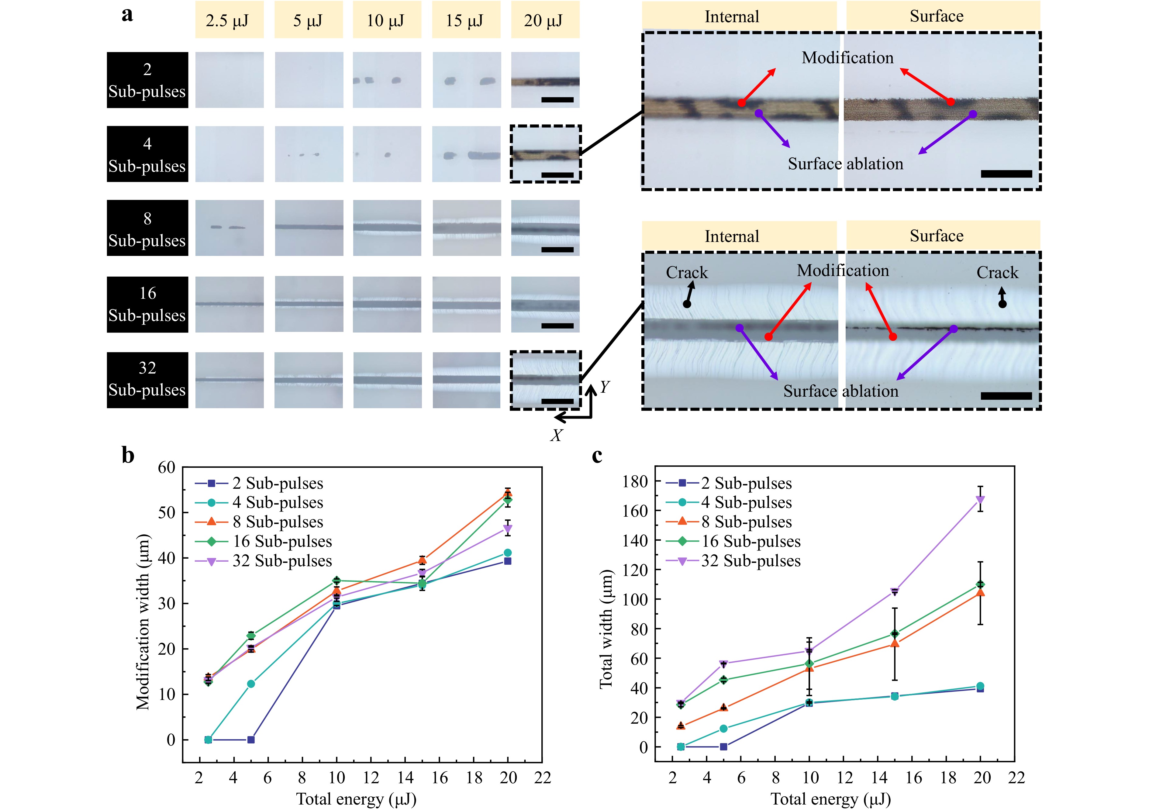
Fig. 2 Single-line writing by scanning procedures with different sub-pulse numbers and total energies. a Top view of produced modifications and microcracks. The scale bar represents 100 μm. The enlarged images on the right presents microscopy observations with image focusing inside and at the surface of the material. b Modification width of the studied parameters. c Total width of affected zones including the surrounding microcracks of the different parameters.
Fig. 2b shows the widths of laser-written lines for different pulse energies (total energy of all applied sub-pulses) and number of sub-pulses used for irradiation. As the total pulse energy increases, the width of the modified lines also increases. However, at the same total energy, the width of the modifications does not differ by more than 20 μm with different numbers of sub-pulses.
Fig. 2c shows the overall width of the zones including the region surrounding the written lines in which the microcracks is observed. Again, as the pulse total energy increases, the overall width of the affected zone of the crystal became wider. However, there are more significant changes of the overall width when the number of sub-pulses is varied. For example, with 32 sub-pulses, the width of the modification-crack affected zone exceeds 160 μm, which is more than four times larger than the modification observed with 2 sub-pulses (~36 μm).
Therefore, the width of the modification line in the crystal is mainly controlled by the applied total energy, while the crack propagation width is influenced by both the total energy and the number of sub-pulses in pulse trains.
Next, we performed continuous multi-line scanning. Fig. 3 shows internal modifications for 4, 8, and 16 sub-pulses for different total pulse energies. The results of multi-line modifications with 2 and 32 sub-pulses can be seen in Fig. S2.
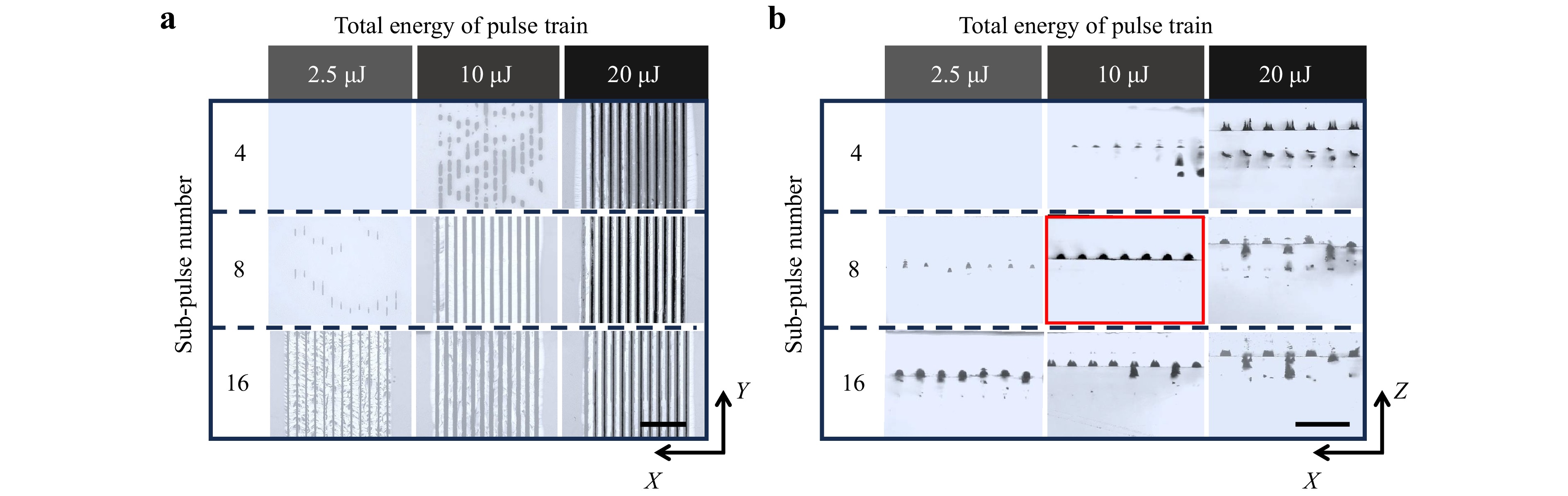
Fig. 3 Multi-line writing by scanning procedures with different sub-pulse numbers and pulse energies. a Top view of produced modifications and microcracks. The scale bar represents 400 μm. b Side view of the modifications and microcracks. The scale bar represents 200 μm. The scanning interval between tracks is 80 μm.
Fig. 3a presents top views of the modified layers. The first observation is that low total energy and sub-pulse number result in unstable internal modification and crack formation in SiC. Higher total energy or sub-pulse number lead to stable modification writing and microcracks formation. At 2.5 μJ, pulse trains with 16 sub-pulses are needed for stable modification and microcracks formation. At 20 μJ, all considered sub-pulse numbers shown in this figure permit internal modification and microcracks extension but one can also noticed it is accompanied by surface ablation features. Fig. 3b shows side views of the modified layers. This reveals additional more details on the modification morphologies. With 4 sub-pulses, low total energy causes unstable modification writing and crack extension, while high total energy causes multiple-layer modification and surface ablation. With 8 sub-pulses, low total energy induces modification without surrounding crack regions, and high total energy still causes multiple layer modification. At 10 μJ, optimal modifications extended by cracks connecting them are achieved without the occurrence multiple affected layers. The overall thickness of the modified region is about 25 μm in this case. With 16 sub-pulses, multiple-layer modification occurs for all tested pulse energies, with ablation layers consisting of tiny modifications below the crack layer. This multilayer modification increases material loss during wafer slicing. Therefore, adjusting sub-pulse number and pulse total energy controls single-layer modification, reducing material loss. In addition, it is observed that the topmost modified layer gradually approached the crystal surface as the total energy increased, indicating that the laser energy deposition point shifted towards the pre-focus direction. This is consistent with previous experimental results reported for internal structuring of SiC27.
We then optimized the scanning speed and interval using 8 sub-pulses with a total pulse energy of 10 μJ. As shown in Fig. S3 and Fig. S4, both excessively low and high scanning speeds fail to produce a stable, single-layer modification. Similarly, a small scanning interval leads to laser pulses blocking by cracks created by previous irradiation, which can then cause their retro-reflection and result in a double-layer modification. Conversely, a larger scanning interval does not adequately promote crack propagation, complicating the subsequent wafer slicing process. Experimental results indicate that a scanning speed of 700 μm/s and a scanning interval of 80 μm enable the formation of a stable single modification layer, effectively minimizing material loss. Cross-sectional characterization of the modified crystal further reveals that the minimum thickness of the laser-modified layer 16.5 μm can be achieved with these parameters.
-
The modification results indicate that the number of sub-pulses for irradiation and the applied total energy are two parameters which are significantly affecting the internal structuring process of SiC crystals. Since SiC is a semiconductor, a direct way to study energy deposition is observing luminescence signals from free-carrier created by nonlinear absorption. The region that produces luminescence is attributed to the zone where carriers are locally excited. By real-time microscopy observation of the luminescence inside the crystal, one can then indirectly examine the deposited energy distributions by the focused laser beam within the crystal. Compared with pump-probe absorption techniques, it is known that lower concentration of carriers can be detected by the luminescence microscopy, and then the pre-focal nonlinear effects can be revealed with more details33. Accordingly, we conduct side luminescence imaging of processed SiC with our focused radiations. To enhance luminescence signals, the repetition rate is set to 10 kHz and the exposure time of the camera to 1/7 s for these measurements.
Fig. 4a shows internal luminescence images for different irradiation energies and sub-pulse numbers. As the total energy increases, the luminescence excitation region gradually expands, mainly towards the pre-focal region. This phenomenon is particularly obvious for the case corresponding to single-pulse excitation. It is similar to the plasma shielding effect observed in previous studies for other semiconductor materials21,34. At a lower pulse total energy of 300nJ, it is interesting to note that the excited region generated by single-pulse irradiation is larger and the luminescence intensity is stronger compared to pulse-train excitations. This can be attributed to the lower intensity of individual sub-pulses with the burst-mode of irradiation and not reaching the threshold for nonlinear carrier excitation for detectable signals. When the pulse total energy increased to 450 nJ, the maximum luminescence signal obtained from 8 sub-pulses is nearly the same as that from single-pulse excitation but with much weaker pre-focal excitation. While operating with the same irradiation total energy with the 32 sub-pulses, significantly weaker excitation remains observed. However, when the pulse total energy increases to 600 nJ, the maximum luminescence signal obtained from single-pulse excitation does not further increase in contrary to multi-pulse cases. The maximum luminescence intensity levels in measured images are then extracted for different conditions for the number of applied sub-pulses and irradiation energies and compared in Fig. 4b. For single pulses, luminescence increases sharply until 350 nJ, then slows, with a 395.8% increase from 50nJ to 350 nJ but only 6.4% increase from 350 nJ to 650 nJ. In practice the observations are consistent with a plasma shielding effect for total energy above 350 nJ causing an elongation of the excited region and a saturation of the achievable internal energy densities. With 8 sub-pulses, luminescence signal exhibits a saturation at higher total energy levels according to signal slowly growing above 550 nJ. At 32 sub-pulses, luminescence signals steadily increase up to 650 nJ without any saturation. Increasing sub-pulse number then apparently reduces plasma shielding, thus improving focal energy deposition.
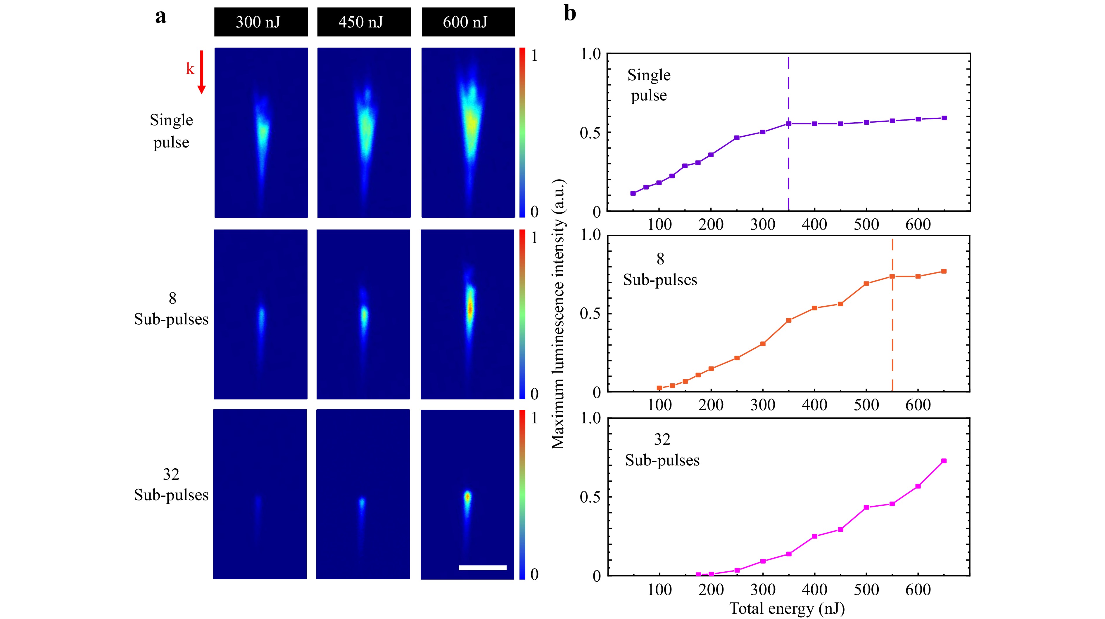
Fig. 4 a Internal luminescence images for varying total energies of single pulse or pulse train and sub-pulse numbers for irradiations. The scale bar represents 20 μm. b The maximum of luminescence signal distributions (normalized) measured for total energy from 50 nJ to 650 nJ comparing the response for single pulse, and with trains of 8 or 32 sub-pulses.
Further characterization of the pre-focal plasma responses was conducted. Fig. 5 shows side luminescence imaging for irradiation with 8 sub-pulses while increasing the total energy. For these experiments, the laser repetition rate is set to 1 kHz, the CCD adjusted gain to 48 dB, and exposure time to 1/32 s. As the total energy increases from 1 μJ to 3 μJ, pre-focal luminescence strengthens. As shown in Fig. 5e, at 3.2 μJ, internal modification and crack induction occur at a plane located prior to geometrical focus, blocking energy delivery for the subsequent irradiations in this pre-focal modified-crack region. Fig. 5f shows an image taken 62.5 ms after the one in Fig. 5e, where it can be observed that repeated irradiations only cause the modified layer to grow upwards. Fig. 5g is a magnified view of the red circle in Fig. 5f. Below the crack-modified layer, carrier luminescence is still visible, indicating that the incident laser is still depositing energy beneath the modified layer. Therefore, we speculate that the multi-layer modification beneath the crack layer, caused by a higher number of pulses or greater energy, is due to the remaining light reaching the focal point after propagation trough the pre-focal crack layers.
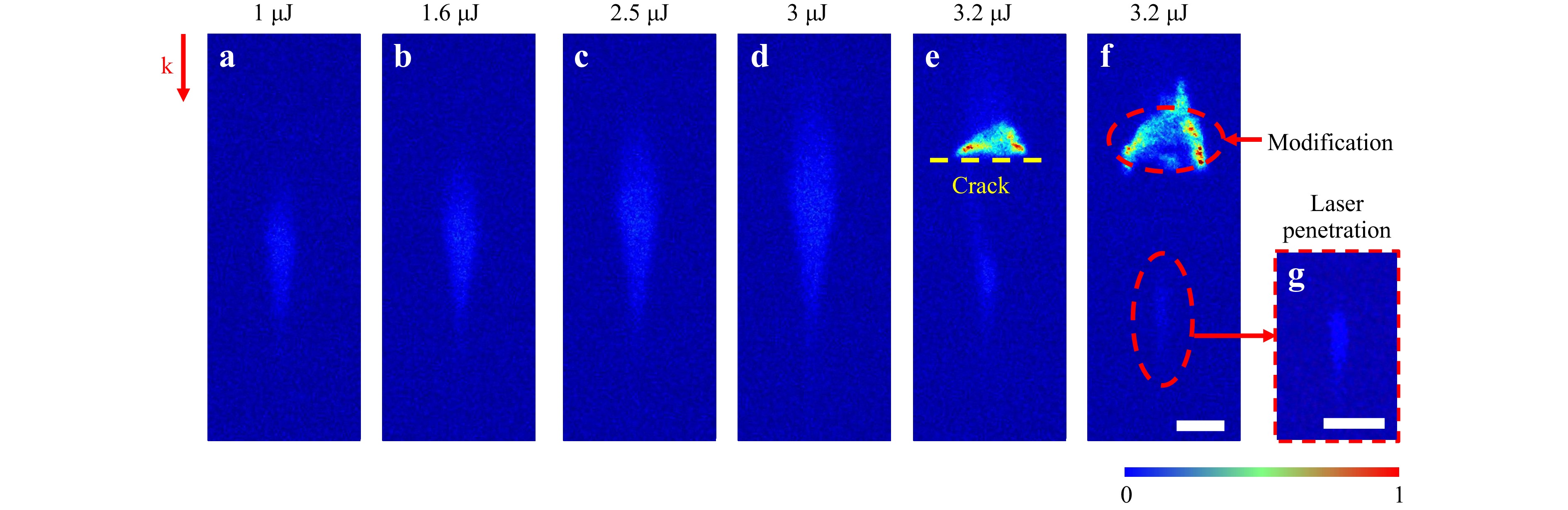
Fig. 5 Internal luminescence images with different total energies for burst-mode irradiations with 8 sub-pulses. The scale bar represents 25 μm.
Based on the above experimental results, we associate the modification experiments in Sec. 3.1 with the following scenario. As sketched in Fig. 6, when using unshaped, low-repetition-rate (kHz) femtosecond lasers for focusing inside a crystal, the high peak power of the pulses causes strong nonlinear effects before the beam reaches the focal point. This results in important carrier excitation in the pre-focal region, where a significant portion of the laser total energy is consumed, spread over a large zone along the laser propagation path. Under these conditions, additional energy only excites carriers above the pre-excited zone rather than boosting the deposited energy density at the focal point.
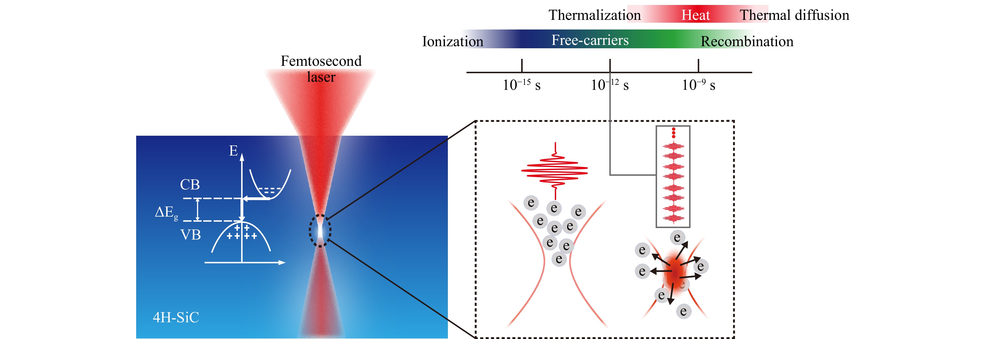
Fig. 6 Schematic representation of expected accumulation effects in SiC. In silicon carbide (SiC), the energy deposition effects vary significantly between different modes of irradiation.
In contrast, when the same laser total energy is applied using ultrafast pulse trains (rather than single pulses), the decreased peak power for each applied sub-pulse effectively suppresses nonlinear effects in the pre-focal region, ensuring that carrier excitation occurs closer to the laser focal point. The free-carrier lifetime $ {\tau }_{R} $ in semi-insulating SiC varies in the range of 1.5-2.5 ns35. With sub-pulse temporal separations in the picosecond range, successive pulses continue to induce photoionization before carriers from earlier pulses have recombined and so carrier can effectively accumulate. Using a simple estimate of the thermal diffusion time $ t={l}^{2}/D $ associated with a length scale $ l $ = 2 μm (the typical dimension of focus), the thermal diffusivity coefficient for 4H-SiC at $ D $ = 1.7 cm2/s leads to 23.5 ns for thermal energy to diffuse away from the interaction region. Then we can conclude that the pulse train allow efficient local thermal accumulation. Depending on the number of sub-pulses, the local carrier density can then accumulate up to a critical level for which material modification within the crystal is obtained. However, when the laser energy deposition becomes too strong, as seen in the experiment when the number of sub-pulses exceeds 8, modification can occur while simultaneously causing carrier excitation and possibly secondary modification sites below the modified layer.
In summary, ultrafast trains of pulse is shown to reduce nonlinear effects in the pre-focal region, thereby increasing the energy density achieved at the focal point, which promotes material modification. However, excessive energy deposition can trigger new nonlinear effects, leading to multi-layer modification beneath the main modification layer.
To compare the effects of the temporal shaping method and the pulse duration extension method, we performed additional luminescence observation experiments. The corresponding experimental results and mechanism interpretations are provided in the supplementary information (Fig. S5).
-
Building upon our findings and understanding of SiC laser processing, we subsequently evaluated the feasibility of implementing a wafer-slicing process via large-area scanning with optimized laser parameters. For these experiments, we utilized a selected portion of a 6-inch wafer, with the irradiated area exceeding 15 cm2. Fig. 7a shows the processed wafer, while Fig. 7b presents an optical microscope image of the surface after slicing for which we can clearly distinguish the laser-modified regions (dark lines) from the crack propagation region (between dark lines). Confocal microscopy image of the sliced surface (Fig. 7c) reveals a relatively low surface roughness, with a line roughness Ra of 0.604 μm (the red dotted line in Fig. 7c). The thickness of the sliced wafer is 160 μm, with cross-sectional characterization shown in Fig. S6.
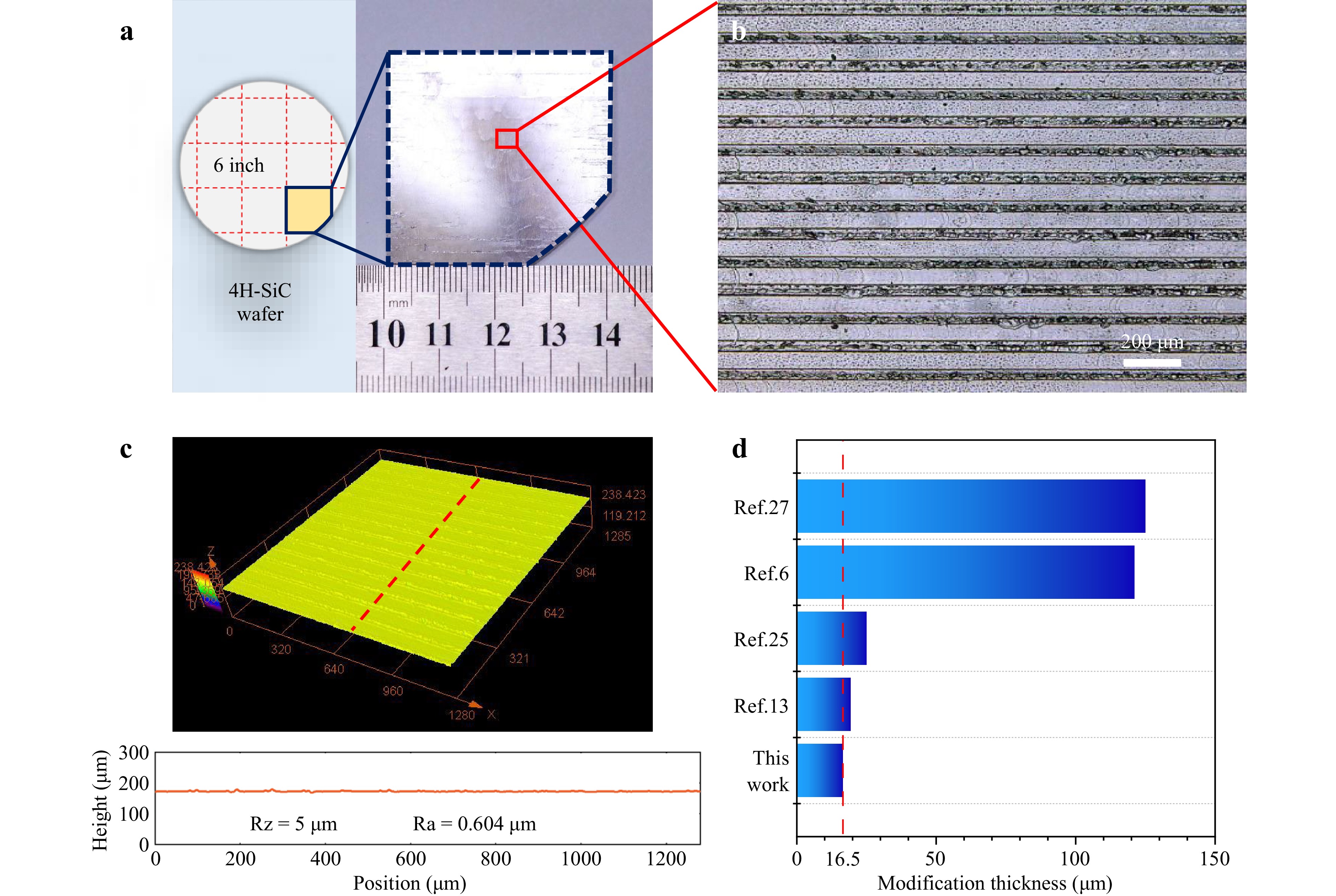
Fig. 7 SiC slicing after large-area scanning of a wafer with ultrafast trains of pulses. a Top view of SiC wafer before slicing. b Top view of optical microscope after wafer slicing. c Confocal microscopy characterization and roughness measurement of sliced wafer surface. d Modification thickness of different works.
Comprehensive surface characterization of the sliced crystals was achieved through scanning electron microscopy (SEM) and Raman spectroscopy analysis. The results are shown in Fig. S7 and Fig. S8. In comparison to other studies on SiC wafer slicing6,13,25,27, our sliced wafer tend to demonstrates higher surface quality and significantly reduced the laser modification thickness. To support the conclusion of a process taking benefit for the burst-mode irradiation approach, Fig. 7d directly compares the laser modification thicknesses reported in this and other previous works.
-
This study systematically investigates temporally shaped ultrafast laser processing for high-precision internal modification of silicon carbide (SiC) crystals. Fig. S9 shows the research block diagram. By using temporally shaped ultrafast pulse trains generated via birefringent crystal stacks, we demonstrate better control over material modification thickness and crack propagation, advancing the potential of laser-based SiC wafer slicing. The key conclusions are summarized as follows: (i) The obtained experimental results show that the characteristics of the produced train of pulses can significantly influence the internal modification and the crack extensions inside the material. By adjusting the sub-pulse number and total energy of the applied pulse trains, we have demonstrated that single-layer modification-crack growth can be effectively controlled, to achieve thickness under 20 μm and so potentially reduce material loss for wafer slicing. (ii) Side luminescence imaging experiments reveal the underlying differences between pulse characteristics and the capacity of the burst-mode to minimize the pre-focal plasma shielding effects. (iii) We successfully sliced a SiC wafer. The thickness of the sliced wafer is 160 μm, and the surface line roughness reaches Ra0.604 μm, which indicates that the wafer with better surface quality can be obtained by using the laser modification and slicing method proposed in this paper. Beside the application of SiC slicing, this study directly supports the potential of ultrafast temporally shaping to offer new control parameters for improving the performances of femtosecond laser process technologies.
-
This work was supported by the National Key R&D Program of China (No. 2022YFB4601300), the National Science Fund for Distinguished Young Scholars (No. 52325505), the National Natural Science Foundation of China (No.52488301), National Key R&D Program of China (No. 2024YFB4609801) and Teli Student Science and Technology Innovation Team Project under the Science and Technology Innovation Program of Beijing Institute of Technology (2024CX06005).
High-precision laser slicing of silicon carbide using temporally shaped ultrafast pulses
- Light: Advanced Manufacturing , Article number: (2025)
- Received: 19 January 2025
- Revised: 29 July 2025
- Accepted: 13 August 2025 Published online: 09 October 2025
doi: https://doi.org/10.37188/lam.2025.065
Abstract: The advent of laser-assisted methods for material slicing attracts a particular attention for technologically important materials as silicon carbide (SiC). Using femtosecond lasers, one can locally initiate multiphoton ionization inside SiC, leading to internal material modifications for slicing SiC ingots into individual wafers. However, intense focused light inside SiC suffers from strong nonlinear effects, such as plasma shielding and self-focusing, which limit energy localization and affect the quality of internal modifications. In this research, we employ temporally-shaped ultrafast trains of pulses for semi-insulating SiC crystal modification. These are generated through an engineered stack of birefringent crystals and permitted successfully slicing a SiC wafer. By adjusting laser parameters, we demonstrate improved energy deposition near the laser focal point and find an optimal combination of laser energy (total energy of pulse train: 10μJ) and number of sub-pulses (8 sub-pulses) to achieve thin single-layer modifications and cracks (thickness: 16.5μm). The suppression of pre-focal plasma shielding and improved control for energy deposition inside crystals are confirmed by side-view luminescence microscopy. Ultimately, the benefits from the technique allow a reduction of the modification layer down to 16.5μm, corresponding to an important advancement for low material-loss SiC wafer slicing.
Rights and permissions
Open Access This article is licensed under a Creative Commons Attribution 4.0 International License, which permits use, sharing, adaptation, distribution and reproduction in any medium or format, as long as you give appropriate credit to the original author(s) and the source, provide a link to the Creative Commons license, and indicate if changes were made. The images or other third party material in this article are included in the article′s Creative Commons license, unless indicated otherwise in a credit line to the material. If material is not included in the article′s Creative Commons license and your intended use is not permitted by statutory regulation or exceeds the permitted use, you will need to obtain permission directly from the copyright holder. To view a copy of this license, visit http://creativecommons.org/licenses/by/4.0/.

 DownLoad: