


-
Photonic Integrated Circuits (PICs) have been long proposed to provide a post-“Moore’s Law” route to high-speed, high-efficiency, high-density and low-cost computation and communication devices1,2. In particular, monolithically integrated PICs, where optics, optoelectronics and electronics are integrated onto a single wafer have long been pursued3,4, yet a fundamental tension remained between the highly scalable silicon-based technology and the challenges of hetero-integration of an electrically pumped coherent light source onto a silicon back plane5. While chip-hybrid, flip-chip and off-chip approaches have seen considerable advances, a seminal 2025 step by de Koninck and colleagues at IMEC showed that high quality, epitaxially grown, electrically pumped lasers on 300 mm silicon could be produced on a CMOS pilot line6 through development of high quality nano-ridge heteroepitaxy. This first demonstration emphasized the potential for on-chip waveguide-coupled emission; now, a new work in Light: Science & Applications by Fahmy and co-workers has shown that silicon integrated nano-ridge structures can also be used to tackle a more traditional need; low-cost, high-density surface-emitting lasers7, through optical engineering with a one-dimensional photonic crystal.
Solid-state laser technology has long relied on the traditional edge emitting technology–providing high powers with relatively poor beam profile–and more recently vertical cavity surface emitting lasers (VCSELs)–providing high density integration and high efficiency with high quality modes. The 1999 report from Imada of two-dimensional lasing from photonic crystal structured materials kickstarted a new paradigm8 of photonic crystal surface emitting lasers (or PCSELs) which continues at pace today9,10. PCSELs have the potential to merge the advantages of both edge-emitting lasers–high powers–with those of VCSELs–high density of integration. This is achieved by imposing a photonic crystal structure onto a gain material, providing optical coupling over large areas through generation of a standing-wave at a photonic band singularity, providing a band-edge effect where group velocity is close to zero and leads to advantages including low threshold, single mode operation, high power and low divergence11. To achieve these benefits, the majority of reports to date implement PCSELs directly in compound semiconductors10 rather than through silicon integration.
The principle of coupling of separate gain material with silicon photonic crystals to achieve lasing is not new12-14. The challenge to-date has been the need to separately form gain material and photonic crystal, following by complex integration, often leading to small area devices with low yield. In their new work7, Fahmy and colleagues make the important step of combining their earlier highly scaled hetero-integration with an intrinsic photonic surface which was grown and prepared in a single step, as shown in Fig. 1a, b. The key enabling step for nano-ridge lasers on silicon was through the careful control of the size and placement of the silicon mask prior to epitaxy (known as aspect ratio trapping); these are inherently a one-dimensional high-index contrast photonic crystal that can be prepared and fabricated at the 300 mm wafer scale.
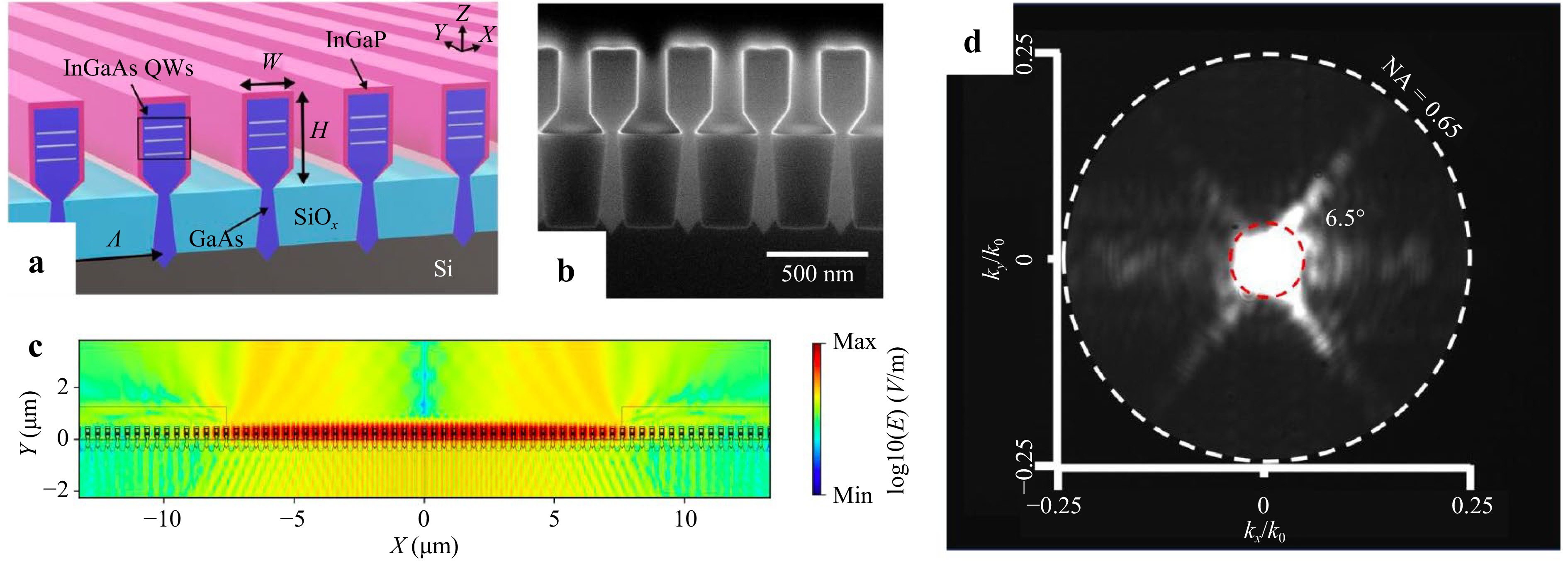
Fig. 1 a The design of the nano-ridge array forms a natural 1D photonic crystal. b An SEM image shows the realized structure. c Simulations predict strong vertical emission. d The measured far-field emission pattern confirms a highly directional beam with a low divergence of 6.5° (Images adapted from Ref. 7).
In their work, the authors demonstrated an optically pumped laser that operates on this principle. However, a clear path to electrical injection via p-i-n junction is feasible building on the authors’ own recent work6. Furthermore, their design shows the potential for emission tunability and low far-field divergence (Fig. 1c, d) through optimization of geometrical parameters. By successfully integrating two technologies, silicon-integrated heteroepitaxial lasers and photonic crystal surface emission, the authors have begun to close the gap between conventional edge-emitting laser and VCSEL capability while simultaneously providing the potential for true CMOS line laser production on 300 mm wafers. This platform promises to be a versatile, tunable, and scalable approach to developing lasers required for the next generation of applications15.
Scaling-up surface-emitting epitaxial lasers on silicon with one-dimensional photonic crystals
- Light: Advanced Manufacturing , Article number: 19 (2026)
- Received: 04 October 2025
- Revised: 05 January 2026
- Accepted: 07 January 2026 Published online: 19 March 2026
doi: https://doi.org/10.37188/lam.2026.019
Abstract: Directly growing III-V lasers on 300 mm silicon wafers is a crucial step for future photonic integrated circuits. While recent work has achieved electrically-pumped in-plane lasing, new research has shown that surface emission can be efficiency achieved by modifying the heteroepitaxy of InGaAs/GaAs nano-ridges to form a one-dimensional photonic crystal, opening a new direction for scale-up of high-density surface emitting lasers on silicon.
Rights and permissions
Open Access This article is licensed under a Creative Commons Attribution 4.0 International License, which permits use, sharing, adaptation, distribution and reproduction in any medium or format, as long as you give appropriate credit to the original author(s) and the source, provide a link to the Creative Commons license, and indicate if changes were made. The images or other third party material in this article are included in the article′s Creative Commons license, unless indicated otherwise in a credit line to the material. If material is not included in the article′s Creative Commons license and your intended use is not permitted by statutory regulation or exceeds the permitted use, you will need to obtain permission directly from the copyright holder. To view a copy of this license, visit http://creativecommons.org/licenses/by/4.0/.

 DownLoad: