


-
Recent advances in optical sensing, imaging, and photonic devices have led to growing demand for optical components that combine compactness, versatility, and high performance1,2. Free-form optics—optical elements with asymmetrical, non-rotationally invariant surfaces—have established themselves as a key technology in this field, as they offer unparalleled flexibility in adapting light propagation, minimizing system size, and enhancing device functionality3. Compared to conventional spherical or aspherical elements, free-form optics offer greater freedom in tailoring the surface geometry across multiple axes, allowing designers to correct complex, field-dependent aberrations and significantly reduce the number of elements in a system. In contrast to conventional lenses, where the surrounding device often has to be adapted to predetermined geometries, free-form optics offer a more flexible approach. They can be shaped to meet the mechanical, electrical, or ergonomic requirements of a specific application, allowing for significantly greater design freedom, especially in scenarios where non-optical components are difficult to modify. Consequently, free-form optics enable novel compact architectures for applications ranging from biomedical imaging to autonomous sensing and augmented reality where performance must be maintained within strict size, weight, and power constraints4.
However, the fabrication of free-form optical elements remains a major challenge. Standard techniques such as ultraprecision machining, polishing, and ion beam processing are limited by material compatibility, surface complexity, and production costs, restricting their use to specialized laboratories and high-end industries5. Similarly, laser-based fabrication methods, while offering high precision, involve high acquisition costs, stringent environmental requirements, and considerable technical expertise, also limiting their use to specialized facilities. Furthermore, the need for iterative prototyping during the optical design process increases time and cost, thereby hindering innovation. Recently inkjet printing methods demonstrated their capacity to manufacture optical components6,7, but devices and resins remain expensive and dedicated to specialists. To overcome these limitations, additive manufacturing8, particularly liquid resin vat photopolymerization techniques such as stereolithography (SLA) and digital light processing (DLP), has increasingly attracted attention as a promising platform for the fabrication of complex optics9–11. These methods enable the rapid, cost-effective, layer-by-layer fabrication of transparent polymeric structures with virtually any geometry, using benchtop printing systems that are widely available and affordable even for non-specialists. The first printers appeared in the 1980s, but the technology’s popularity did only grow massively after the expiration of the first patent12. This combination of simplicity, low cost, and design flexibility provides a powerful tool for iterative, on-demand prototyping and small-scale production13.
Despite these promising prospects, several critical challenges remain before 3D-printed optics can meet the stringent requirements of optical applications. The quality of printed elements is often compromised by several factors, including insufficient optical clarity, high surface roughness, and material autofluorescence. All these issues can contribute to a reduction in device performance. Furthermore, the refractive index of photopolymer resins plays a critical role in determining the light-guiding, refracting, or focusing properties of printed optical components. However, there is a lack of available data on commercial materials in this field14–16.
Due to our long-standing focus on the development of miniaturized analytical assays and devices for onsite (bio)chemical analysis and sensing—primarily utilising fluorescence detection—we require cost-effective, application-specific optical systems for the readout of test strips, lateral flow assays or microfluidic chips. These systems require light-tight housings and integrated excitation and emission optics, which we often manufacture using 3D printing. In particular, the fabrication of free-form, transparent optical elements with minimal autofluorescence (when excited in the deep blue) has become a key aspect of our work. To ensure affordability and accessibility, we focus on the use of commercially available resins and filaments that are compatible with desktop 3D printers. This motivated us to conduct a comprehensive spectroscopic, optical, and morphological study of six transparent resins suitable for SLA printing based on Liquid-Crystal Display (LCD) technology, which are readily available from online retailer platforms. We characterized their light transmittance, autofluorescence, refractive index and surface quality, and established a robust post-processing protocol that significantly improves optical performance.
Based on these findings, a simple and fast method for producing optical elements was developed and validated through practical applications. Three fluorescence sensor systems from previous works—each requiring miniaturized, aspherical or free-form lenses—were selected as test cases17–19. In these systems, the original glass optics were either replaced by 3D-printed resin replicas (“twins”) or by newly designed free-form optics tailored to the specific sensor geometry. The resin twin lenses showed a high match with their glass counterparts, while the custom-designed free-form optics led to a significant improvement in performance. As an introductory proof of concept, Fig. 1 shows the rapid prototyping of a retroreflector prism, highlighting the potential of this approach to make the development of low-cost, customized optical components widely accessible. This work impressively demonstrates how 3D printing workflows that can be deployed in almost any laboratory can support the advancement of integrated optics, biosensing, microfluidics and other light-based technologies.
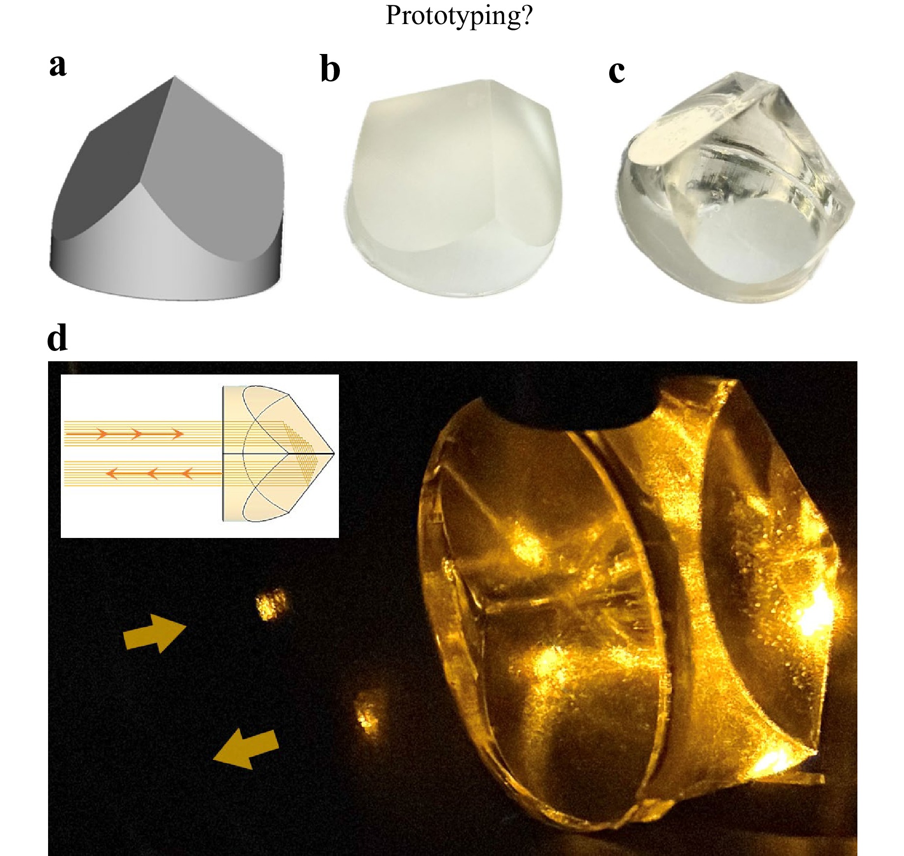
Fig. 1 Successive stages in the fabrication of a retroreflector prism for optical applications: a computer-aided design; b SLA printed element; c element after post-treatment; d retroreflection of a laser beam at 589 nm by the manufactured optical element shown in c.
-
Six colourless commercial resins were purchased: Siraya tech simple – Water washable (resin 1) (Siraya tech); Superfast clear (resin 2) (3D Materials); High clear resin (resin 3) (Anycubic); Clear impact (resin 4) (Liqcreate); High Clear Resin (#3124) (resin 5) (IFUN); Standard photopolymer resin translucent (resin 6) (Elegoo).
The characterization of the candidate materials was performed with printed bulk rectangular cuboid blocks in the shape of a conventional 10 mm-cuvette’s external dimensions (12.4 × 12.4 × 55.0 mm). Each element was printed on a Phrozen Sonic mini 8K printer (Phrozen) in normal atmosphere. The printed parts are constantly immersed in the liquid resin during the printing process, but are not exposed directly to air during this process. The printing was followed by a washing step (2 min) with isopropanol (isopropyl alcohol, IPA, 98%; Labsolute) to eliminate the excess of resin from the surface of the blocks. For post-processing, to eliminate the printing-related surface artefacts as effectively as possible, the raw objects were coated with mother resin, which was applied using a pneumatic atomisation technique with an airbrush pistol (AFC-101A Double action airbrush pistol Nozzle, diameter 0.35 mm, Conrad) connected to compressed air. At working pressures of 1–3 bar, the 0.35 mm nozzle cap produces a conical spray of droplets of 30–60 µm, consuming approximately 1 mL·s–1 of resin. With a working distance of approximately 10 cm, the spray coated area is around 3 cm in diameter. The smaller objects were coated using a silicon brush to obtain a more efficient finish. In a second step, the coating of the thinly applied resin was cured through photo-polymerization by UV light irradiation in a curing machine (Wash and cure machine 2.0, 405 nm wavelength, Anycubic). For finishing, another washing step (2 min) with IPA was performed to remove possible traces of excess resin, dried with compressed air, and then subjected to a second UV light curing. All the photo-polymerization steps carried out during the post-treatment were performed under normal or inert atmosphere, see details in the Results and discussion section.
The printing parameters were selected according to the specifications of the respective manufacturer and refined iteratively to obtain the best possible printing result for the raw element. An opensource 3D design software (FreeCAD) with the Optics Workbench Addon (v1.0.26) was used for designing the elements and exporting the data to the slicer software (Chitubox, CBD-Tech) for the setting of the printing parameters. The photo-polymerization during the printing process took place under sequential LCD irradiation at 405 nm of the design slices. In the same way, the photo-polymerization during the post-treatment was carried out under constant irradiation at 405 nm.
-
The optical transmittance of the resins was recorded with a Specord 210 spectrophotometer (Analytik Jena). To study the materials’ autofluorescence, an excitation-emission matrix (EEM) analysis was carried out with a Fluoromax 4 fluorometer (Horiba). The excitation range was 400–600 nm (10 nm step size) and the emission was scanned in the range of 410–850 nm (1 nm step size). To avoid inner filter effects (light absorption, scattering, reflection or shielding) that might appear when the fluorescence of bulk blocks with a potentially too high optical density is measured in the conventional 90° configuration, the blocks were measured in front-face configuration with perpendicular excitation to the block surface and an emission collection at an angle of 30° respective to the irradiated surface, collecting only the emission from the surface of the excited sample20,21.
The refractive index was obtained with a customized setup consisting of a 5 mW 589 nm- or 498 nm-laser module as light source and a 3D printed holder with positioning clamps for reproducible mounting and positioning of the optical element. Especially the 589 nm-laser module was used as it corresponds best to the sodium D line which is the standard wavelength used for the determination of the refractive index of glasses22. The refractive index of the resin, n2, was calculated manually according to Snell’s law
$$ \mathrm{n}_{ \mathrm{1}} \mathrm{sin\theta }_{ \mathrm{1}} \mathrm{=n}_{ \mathrm{2}} \mathrm{sin\theta }_{ \mathrm{2}} $$ where n1 = 1 is the refractive index of air, θ1 = 45° is the angle of the incident laser beam and θ2 is the angle of the refracted beam in the printed optical element. θ1 and θ2 were obtained from photographs of the beam path taken with a camera mounted perpendicularly to the beam and traced with the aid of a drawing software (CorelDraw, Corel).
Surface roughness was studied with a laser scanning microscope (Lext OLS5000, Olympus) using ×50 magnification and the respective parameters were calculated using 4 random working areas of 258 × 258 µm2.
To assess the dimensional accuracy (match of 3D-designed and printed objects) and the dimensional reproducibility of the 3D printed structures, parallelism and thickness of the elements were measured with a digital indicator (Digi-met, Helios Preisser) and a digital ruler (digiMax, Wiha), respectively. The dimensional gauges were performed between the parallel sides of the blocks.
-
Two miniaturized opto-analytical devices previously published by us were replicated with the equivalent 3D printed optical components following the developed protocol and resin 1. The first one was a fluorometric test strip-based assay for hydrocarbon detection (Fig. S15)17. Fluorescence was generated using a standard 430 nm light-emitting diode (LED, LED 430-06, Roithner Lasertechnik), which was filtered through a bandpass filter (65622, Edmund Optics) mounted at an angle of 130° to the surface of the strip. The emission from the test strip was collected perpendicularly to the strip, passed through a long-pass filter at 455 nm (5CGA-455, Newport) and focused by an aspheric condenser lens (ACL25416U, Thorlabs) into an optical fibre bundle (BFL200HS02, Thorlabs) connected to a USB spectrometer (USB2000+, ILX-511B detector, OceanOptics). The signal was acquired in the range of 460–650 nm and processed on a laptop computer with the SpectraSuite software (OceanOptics). The second system was a microfluidic chip-based device for monitoring chlorine levels in pools (Fig. S16)18. The excitation source was a 490 nm LED (LED 490-06, Roithner Lasertechnik) filtered with a 500 nm short-pass filter (FESH0500, Thorlabs) and focused on the microfluidic chip with a plano-convex lens (LA1540, Thorlabs). The fluorescence from the chlorine-reactive fluorescent probe flowing through the chip was collected into an optical fibre bundle (BFL200HS02, Thorlabs) after passing through a 515 nm long-pass filter (OG515, Edmund Optics) and focusing with a plano-convex lens (LA1540, Thorlabs). The fluorescence was analysed with the USB spectrometer as above and signal acquisition in the range of 510–650 nm was also made in a similar manner.
For both setups, calibration curves were obtained for increasing concentrations of diluted lubricant oil (LiquiMoly) or sodium hypochlorite (Labsolute) in water, respectively, first with the commercial lenses and then with the replicas prepared from resin 1. Three repeat measurements were made in every case.
For the third miniaturized device, three newly designed free-form optics were added to improve the optical readout of a smartphone-based assay for the rapid detection of microbial contamination of fuels (Fig. S17)19. The new lenses were manufactured following the developed protocol and using resin 1, before being mounted inside a 3D-case, which was printed with black PLA filament using an Ultimaker 3 printer (Freeform4U). For excitation, a 465 nm LED (RLS-B465, Roithner LaserTechnik) was driven by a DC current of 20 mA drawn from the smartphone’s battery via a USB on-the-go (OTG) connection. A 469 ± 18 nm bandpass filter (FF01-469/35-25, Semrock) was placed in the excitation beam and a 500 nm long-pass filter (FEL0500, Thorlabs) between strip and the smartphone’s CMOS back camera, which was used to collect the emission. Photographs were taken with a Samsung Galaxy S7 edge. The smartphone camera was set with a shutter speed of 1/10 s, an ISO gain at 1600 and a white balance at 5000 K. The focus was manually controlled; macro focus without lenses, infinite focus with the lenses. The molecular beacon and complementary RNA sequence were purchased from Eurofins.
-
SLA printing builds 3D objects by curing thin layers of resin using structured light exposure23,24, making it a promising technique for manufacturing transparent optical components with complex geometries25. However, commercially available resins and standard printer settings are typically optimized for structural applications rather than optical quality, so printed objects often lack the transparency required for optical elements. To assess the suitability of commercially available transparent resins, six commercial products were selected (see Experimental Section) and printed using the manufacturer’s standard settings. The resulting rectangular cuboid blocks often showed internal air bubbles and a cloudy, uneven appearance. To improve printing quality, certain process parameters were systematically modified (Table S1). In particular, reducing the speed for all layers significantly improved layer adhesion and minimised the trapping of bubbles (Fig. S1); but to preserve clearness and avoid yellowing of the resin, rapid printing was necessary.
However, even with customized settings, the printed blocks initially had a cloudy, translucent appearance (Fig. S2), which did not correspond to the designation of the resins yielding “clear” or “transparent” prints. Microscopy analysis revealed that the cause was the stair-stepping effect, a well-known artefact of layer-by-layer manufacturing that results in surface roughness that scatters light (Fig. 2a). These results stressed the importance of adjusting both the printing process and the subsequent post-treatment steps to meet optical quality requirements (Fig. S3).
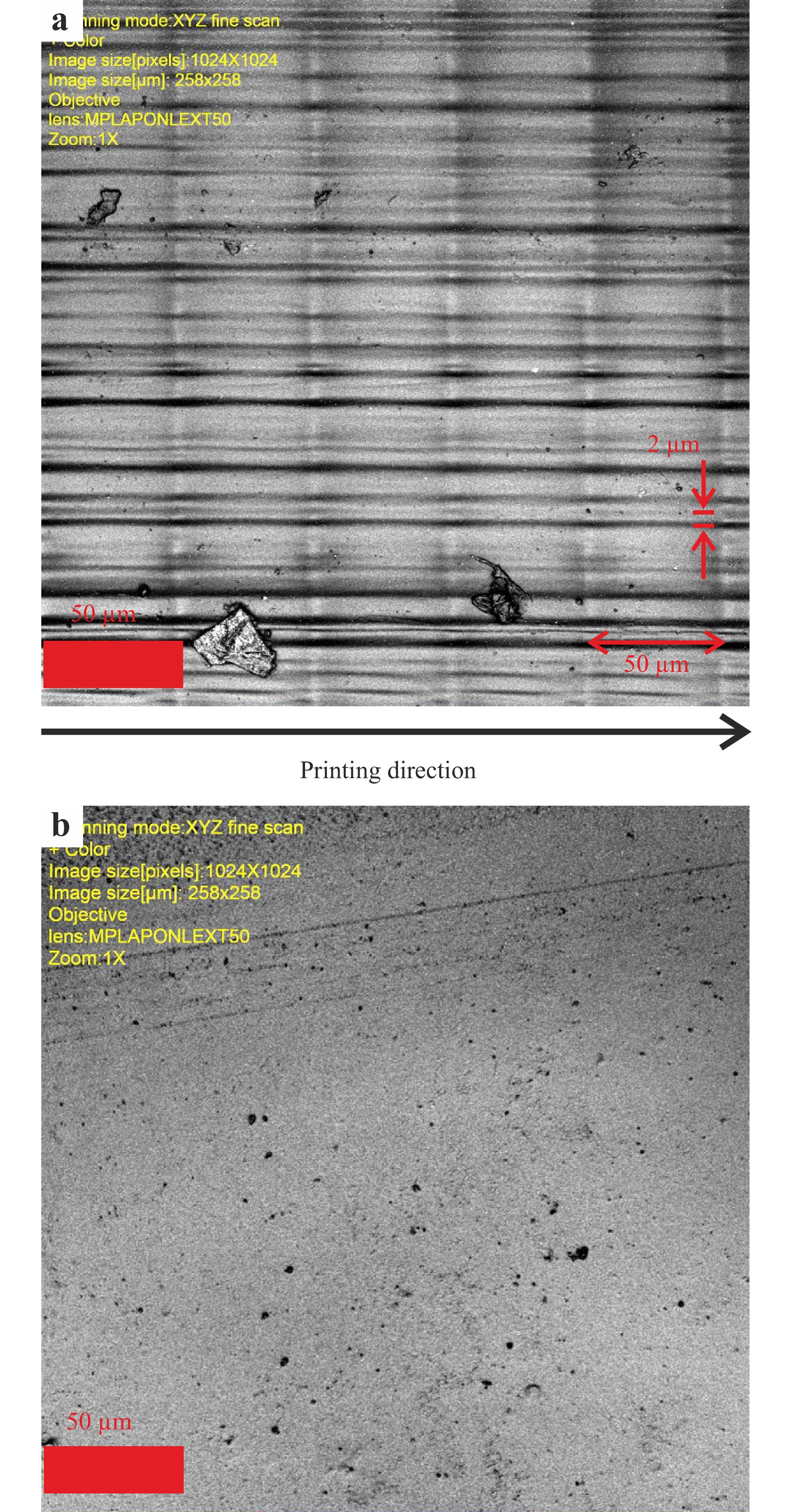
Fig. 2 Laser scanning microscope image (258 × 258 µm), with nominal magnification of ×50, of a 3D printed rectangular cuboid block a without post-treatment and b after post-treatment. The black arrow shows the printing direction in which layers of 50 µm width are built perpendicularly to the printing direction.
As Fig. 2a reveals, the wider recurrent structural patterns on the surface of the object correspond to the pre-set printing layer thickness (approx. 50 µm, in printing direction), while the narrower features of approx. 2 µm are presumably connected to the foci of the microlens array of the light source. Hence, to increase the transparency and smooth the surface a post-treatment is necessary26.
Most reported post treatment procedures are abrasive techniques, which are ultimately followed by coating with a varnish27,28. However, without precision instruments for abrasion, the reproducibility of such methods is hard to control. In addition, the varnish coating results in a thin layer of material on the printed substrate that possesses different optical properties, which is undesirable as it can introduce further complexity, for instance, in case of unmatched refractive indexes. Thus, an alternative post-treatment procedure was developed, utilizing the same UV curable polymerization mixture and applying it in a micrometric layer29. For this purpose, the surface of the printed objects was coated with the respective resin using a pneumatic atomisation technique, whereby fine droplets produce a very homogeneous layer that largely levels out the ridges and valleys caused by printing, resulting in much smoother surfaces. Smaller printed objects were coated using a silicon brush to remove excess of resin applied during spray coating and obtain a better finish. These methods allow to coat indefinite geometries without the limitation that other coating techniques offer, for example, spin-coating, in which a planar surface is needed to apply the resins15,30. A single coating step resulted in a significant improvement of the surface smoothness and the optical properties of the object with respect to the raw object as shown by the laser scanning microscopy images in Fig. 2b and Fig. S5-S9, the macroscopic net effect being visible in Fig. S2. To quantify the post-synthetic improvement, four commonly employed roughness parameters were considered and determined: the root mean square deviation (Rq) and arithmetic mean deviation (Ra) within the sampling length (258 µm) as well as the root mean square height (Sq) and arithmetic mean height (Sa) within the evaluation area (258 × 258 µm)31. Table 1 shows the average of the roughness parameters of five bulk elements printed from the commercial resins. The post-treatment applied during the manufacturing process achieves low and comparable surface roughness values, similar to those obtained through more complex polishing techniques such as laser smoothing, with a surface roughness range of 0.12–0.61 µm, using different types of polymers32. Manufacturing processes for optical glass, such as N-BK7, can achieve higher grades of surface qualities and lower surface roughness values, yet they involve more complex and sophisticated instrumentation33,34. This translates into higher costs, the need for qualified personnel, and longer manufacturing times35.
Resins Ra (nm) Rq (nm) Sa (nm) Sq (nm) resin 1 33 ± 96 52 ± 148 34 ± 13 126 ± 92 resin 2 14 ± 19 20 ± 29 17 ± 3 50 ± 16 resin 3 15 ± 20 22 ± 35 16 ± 3 54 ± 13 resin 4 16 ± 21 23 ± 34 20 ± 7 68 ± 44 resin 5 21 ± 28 33 ± 55 24 ± 3 84 ± 18 resin 6 15 ± 15 20 ± 28 25 ± 25 44 ± 39 Table 1. Roughness average of six 3D printed elements manufactured from six different optically suitable commercial resins for LCD 3D printing using a laser scanning microscope.
Structurally, the manufactured optical elements exhibited dimensional deviations in the micrometre range and parallelism deviations on the order of a few arcminutes (Table S2). This latter deviation is due to a thin meniscus of excess coating resin that accumulates at the lower edge and causes a slight tilt, contributing to angular deviation. In the centre of the optical element, the measured parallelism was 4.3 ± 1.6 arcminutes, which is within the typical specification range for commercial optics (often ≤1–5 arcminutes)36,37. This precision meets industry-level tolerances. For example, precision glass moulding processes routinely achieve wedge tolerances of around 1 arcminute and position alignment errors of a few arcminutes38. Similarly, the deviation between the printed object and its digital design was 22 µm for a set of five cuboids, which corresponds to the expected profile errors in commercially available polymer optics, where dimensional tolerances are often within ±10–50 µm depending on the size of an object and the process parameters36,37. In addition to the cuboids, a set of 10 replicas of a standard plano-convex lens was manufactured following the same protocol (Fig. S4). The obtained optical resin elements showed similar deviation to the commercial glass lens from the design dimension. The respective deviations in height were 154 and 110 µm for resin 1 and commercial glass, respectively, and 147 and 40 µm for the diameter (Table S2). This slightly bigger deviation in diameter is presumably due to a slight excess of resin accumulating at the bottom edge of the lens. In contrary, the coating of resin on the spherical part of the lens appeared optimal and the obtained radius of curvature was 13.07 ± 0.05 mm for a design with a radius of 13.1 mm.
Besides the surface and structural parameters, the inner properties of the printed elements were also checked for compatibility with optical applications. First, the optical transparency was analysed (Fig. 3). Indeed, optical elements require maximal transmittance in the selected spectral range, avoiding power losses. The light transmittance of six rectangular cuboid blocks printed with the commercial resins was evaluated, as it is a discriminatory factor for their use in the optical devices of our test cases. The elements printed with resins 1–5 showed transmittances of 85% for wavelengths above 450 nm, but the transmittance of resin 6 was less than 80% below 500 nm. For the first five resins, the values are only slightly lower than those for standard optical materials such as poly(methyl methacrylate) (PMMA) or N-BK7 glass, which commonly possess transmittances of approx. 90% for 10 mm optical depth39,40.
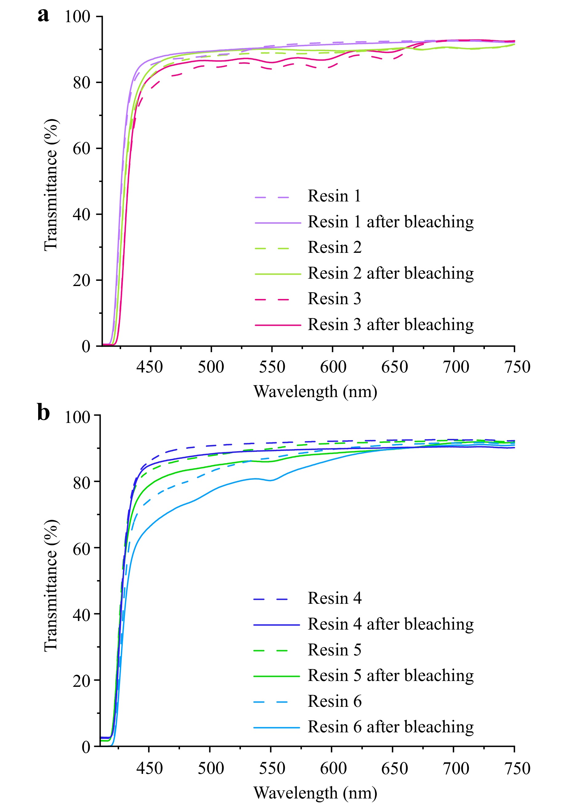
Fig. 3 Transmittance spectra of 12.4 mm thick rectangular cuboid blocks before (dashed line) and after dual wavelength (line) irradiation at 450/550 nm, fabricated from six different commercial resins and post-treated in inert atmosphere: a resin 1 (light purple), resin 2 (light green), and resin 3 (pink); b resin 4 (dark blue), resin 5 (dark green), and resin 6 (light blue).
The limited transmittance can be due to the disruption of the polymerization process by oxygen inhibition, where interaction of the photo-initiators with the oxygen present in air can induce the formation of inactive peroxyl radicals, such as hydroperoxides, or by scavenging the formed radicals41–44. For example, the photo-initiator 2,2-dimethoxy-2-phenylacetophenone frequently leads to photo-yellowing because of cleavage and formation of coloured recombination products during prolonged UV irradiation45,46.
To prevent further detrimental processes from occurring after post-treatment in air, the printed and coated objects were irradiated for 24 h at 450 nm and 550 nm with 36 W, causing the excess of photo-initiator and oxidized reaction products to photo-bleach47–49. As shown in Fig. 3, the bleaching led to an increase of the light transmission of resins 1–3 in the range 440–580 nm. However, resins 4–6 exhibited an attenuation of optical transmittance in the range 440–700 nm, which was most dramatic in the case of resin 6.
After identifying the potentially problematic effects of atmospheric oxygen on the properties of the finished objects, we investigated the extent to which post-treatment of the printed objects in an inert atmosphere (N2 or argon) could be beneficial (Fig. 4, Fig. S10). The first finding was that no noticeable difference was observed between argon or nitrogen with high transmittance from 420 to above 1100 nm for resin 1. While the elements post-treated under air atmosphere needed 20–30 min of curing time and exhibited a fragile surface, those cured under inert atmosphere only needed 1 min curing, resulting in a more rigid surface. Some resins even exhibited shrinkage of the surface coating after less than a minute of curing (Fig. S11). This phenomenon could be due to the shrinkage the polymeric matrix tends to undergo when there is a reduction of the intermolecular distance upon conversion of the free monomer molecules (Van der Waals forces to covalent bond distances) during polymerization and crosslinking50,51. Therefore, the curing time and conditions need to be adapted for every single resin. Attempts to cure in the dark without UV light, but by heating in an oven, resulted in yellowish and brittle elements and were therefore not continued (Fig. S12) In addition, the undesirable formation of yellowish products decreased drastically upon curing in inert atmosphere. The transmittance of all the resins increased significantly apart for resin 6. The resulting transmittance for resins 1–5 reached up to 90%, much closer to standard optical materials properties.
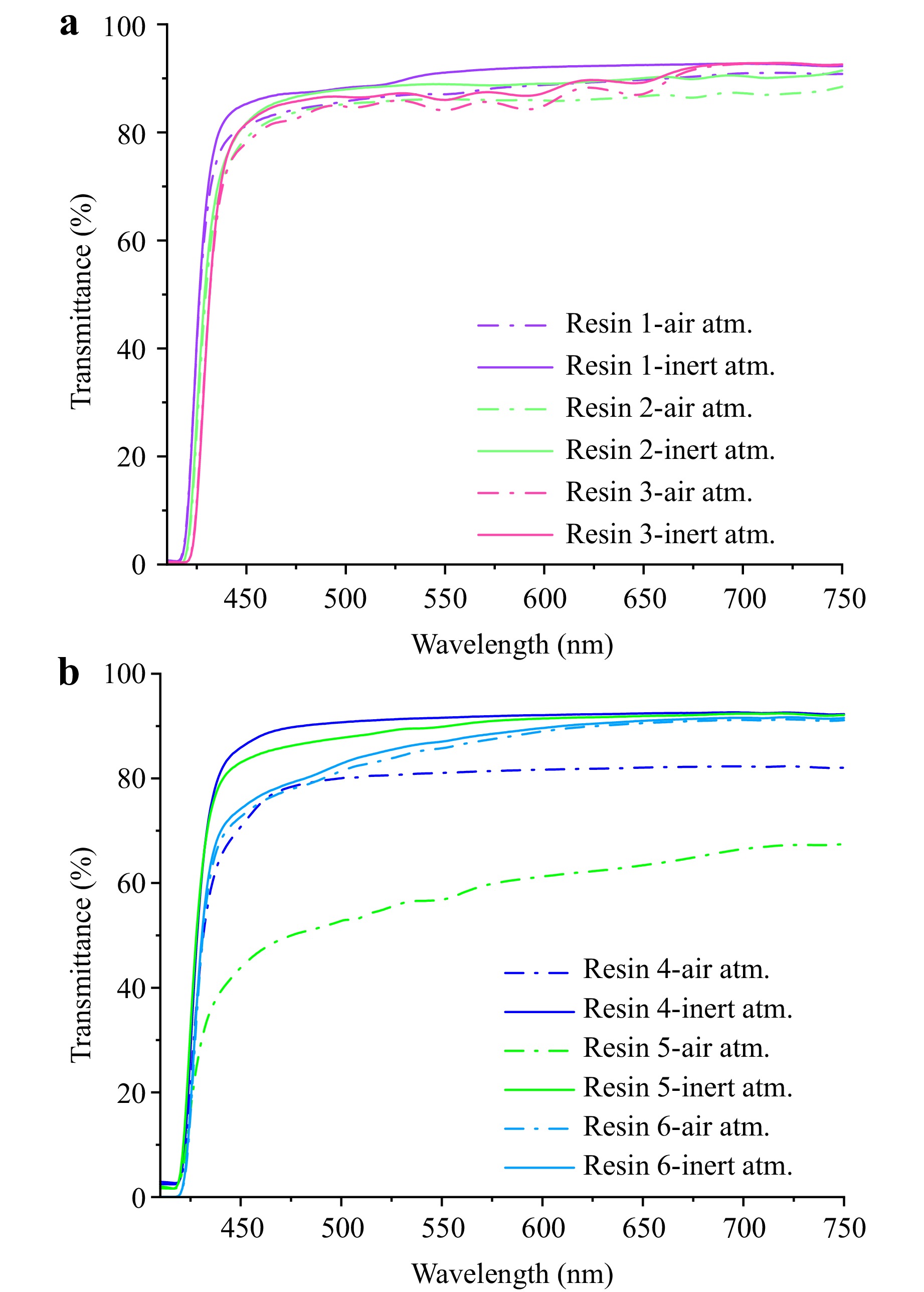
Fig. 4 Transmittance spectra of six rectangular cuboid blocks of 12.4 mm thickness fabricated from six commercial resins post-treated in air (dashed line) and inert atmosphere (line): a resin 1 (light purple), resin 2 (light green), and resin 3 (pink); b resin 4 (dark blue), resin 5 (dark green), and resin 6 (light blue).
For optical elements in general, and especially for optics used in low light application such as fluorescence, the material must have virtually no intrinsic fluorescence background, i.e., autofluorescence should be minimal. The presence of photo-initiators or photo-stabilizers able to emit fluorescence can potentially lead to such undesirable background. Therefore, we recorded excitation-emission matrices (EEM) of resins 1–5 (Fig. 5, Fig. S13). Low fluorescence signals were measured for resins 1–3, especially for resin 2, for which there is virtually no fluorescence in the entire spectral working range. Resin 1 exhibited a fairly intense fluorescence localized at 430–520 nm upon excitation at 420 nm, while resin 3 showed a weak fluorescence between 440–540 nm for excitation wavelengths between 410–440 nm. Resins 4–5 exhibited the highest fluorescence intensity, in the 430–550 nm range upon excitation between 410–440 nm. Although the exact chemical composition of the resins is not known, the sources for the fluorescence are most likely the photo-initiator, since most of them have a sizable molar absorption coefficient in the blue range, corresponding to the LCD printer’s irradiation wavelength, in our case 405 nm52–54, or the photo-stabilizers, also absorbing in the UV.
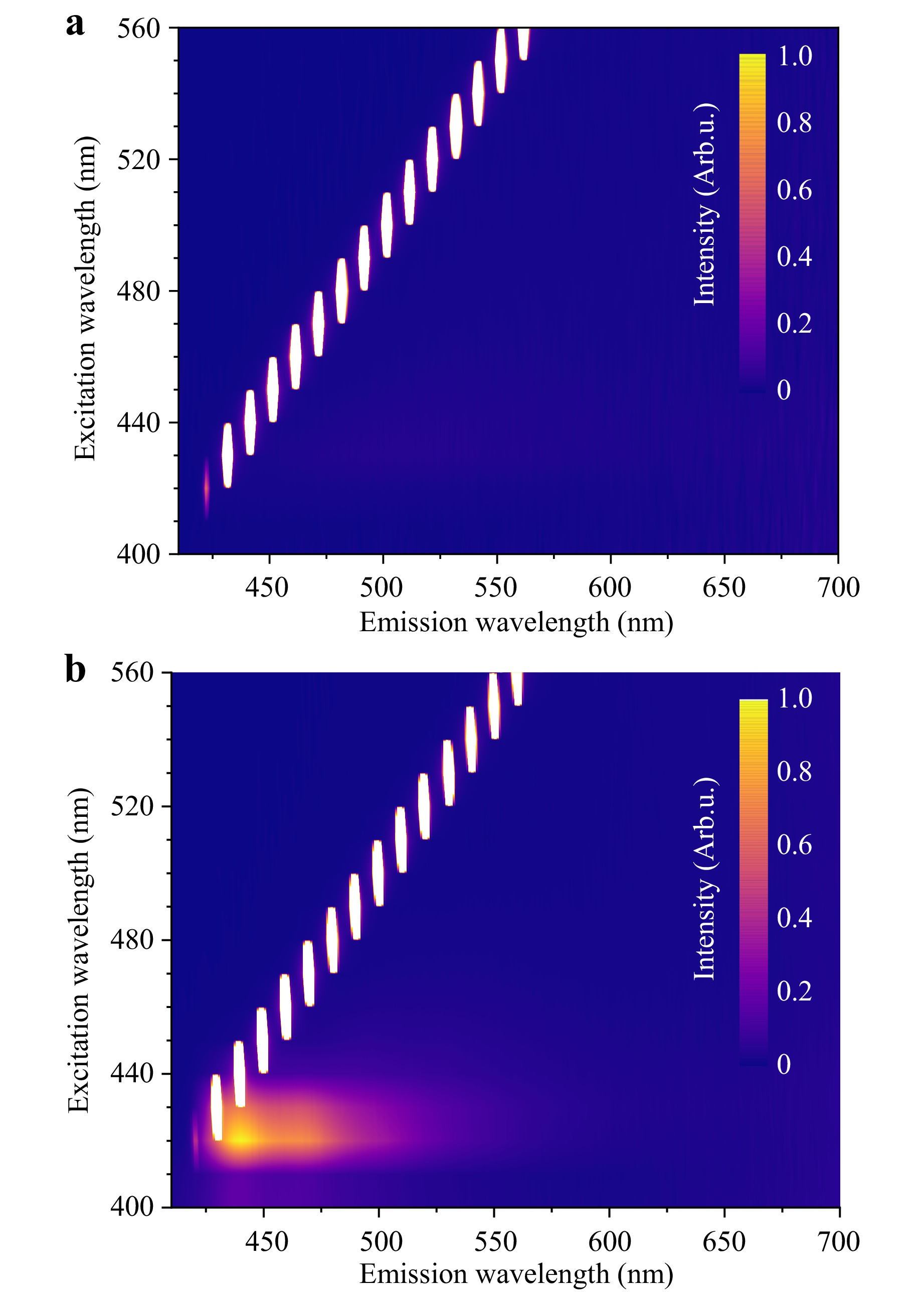
Fig. 5 Front-face excitation-emission-matrices of rectangular cuboid blocks from a resin 2 and b resin 4. Matrices built by successively recording emission spectra within the 410–700 nm range at increasing excitation wavelengths between 400 and 560 nm with steps of 10 nm.
In addition, upon storage in the dark at room temperature in air for two years, the manufactured cuboids showed good environmental stability over time, with an only slight decrease in both, transmittance and autofluorescence (Fig. S14).
The last materials property that is important for optical elements is the refractive index (RI). The RI will determine how the light is refracted by the element and consequently determine the optical component design and the light output direction. The calculated RI for resins 1–5 ranged from 1.44 to 1.53 at 589 nm and 1.50 to 1.52 at 498 nm (Table S3). These values are similar to standard optical polymers (e.g., PMMA or polycarbonate) and optical glasses (e.g., N-BK7) which possess RIs of approx. 1.555. This is an advantageous feature because existing designs for such materials could be directly transferred to the manufacturing with the newly developed method, affording virtually identical optical behaviour.
-
To demonstrate that the optical components manufactured using the post-processing method developed here can compete with conventional optics in terms of performance, we replicated two miniaturised analytical devices we had previously published with the respective 3D-printed optical elements. In addition, we designed a new optical system to improve the sensitivity of a third assay and printed the necessary elements, confirming the improved performance in the experiment.
The first test case was a rapid assay for the detection of total petroleum hydrocarbons (TPHs) in water and soil17. In brief, the assay uses a fluorometric test strip that is sterically coated with a fluorescent molecular rotor dye which exhibits high fluorescence intensity when TPHs are present. For water samples, the protocol involves adding 160 µL of cyclohexane as auxiliary solvent to 40 mL of the water sample, shaking the mixture (1 min) and placing a test strip on its surface to collect the oil. The fluorescence of the strip is then recorded immediately with the device as described in the Experimental Section, and the integrated intensity is compared to a reference strip to calculate the ratio. The optical setup included a commercial aspheric condenser lens which could be easily manufactured following the method described above with resin 1 (Fig. S15, Movie S1). Two calibration curves using the previously described test strips were acquired, one with the commercial lens and the other with the 3D printed twin. As shown in Fig. 6a, the two calibration curves measuring the fluorescence response of the strip upon increasing concentrations of TPHs showed identical trends and a comparable standard deviation (total relative error method)56.
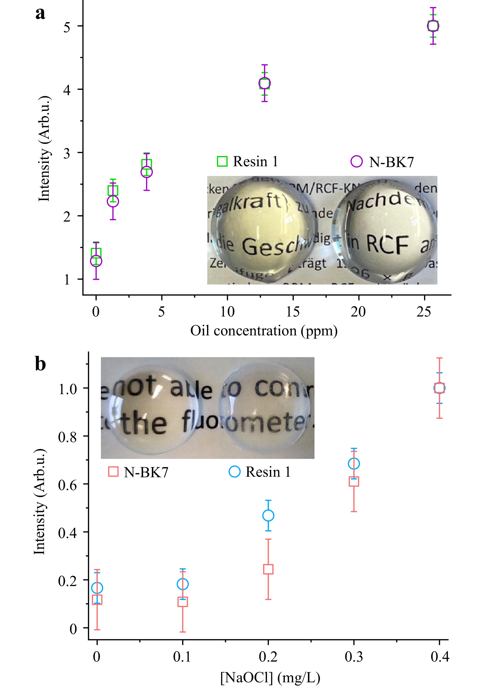
Fig. 6 Response of two miniaturized analytical devices built with glass lenses (purple and red) and resin 1 lenses (green and blue): a test-strip based opto-sensor for hydrocarbon detection with a photograph of the aspheric condenser lenses (Ø = 25.4 mm) manufactured with resin 1, following the method developed here, and made from NBK-7, obtained from the manufacturer (ACL25416U, Thorlabs); b microfluidic sensor for chlorination levels in water with a photograph of the two small convex lenses (Ø = 12.7 mm) manufactured with resin 1, following the method developed here, and made from NBK-7, obtained from the manufacturer (LA1540, Thorlabs).
Likewise, a microfluidic device for the determination of water chlorination levels was built with two small lenses (0.5 inches diameter) with focal length of 15 mm for in-flow probe excitation and emission collection (Fig. S16, Movie S2)18. Both small twin lenses of the commercial ones were manufactured. This assay integrates a microfluidic system, a fluorescent indicator dye which reacts specifically with free and other reactive chlorine species. The device’s design allows for precise mixing of reagents and sample, followed by fluorescence detection, enabling real-time monitoring of water chlorination levels with the fluorescence signal increasing proportionally to the concentration of chlorine species. As shown in Fig. 6b, matching responses were obtained for both setups, with slightly higher repetition errors for the glass lenses that could be due to their enhanced capacity to collect environmental light.
The third test case concerns an improvement of the device initially developed for a dip-stick assay for the rapid, on-site detection of microbiological fuel contamination19. The assay utilizes dip sticks that embed core/shell particles in which the shell is functionalized with molecular beacons. The assay works by detecting the presence of genomic DNA from bacteria and fungi commonly found in contaminated fuels. When this DNA is present, the strands interact with the molecular beacons, leading to a change in fluorescence that can be quantitatively assessed with the optical detection device, indicating the presence of microbial contamination. This system provides a portable and straightforward method for field analysis of fuel quality. Whereas the original setup was very simple in design, basically integrating a light source, two filters and the smartphone camera as the detector, here, free-form optics were designed and manufactured from resin 1 to improve the optical read-out (Fig. 7a, b, Fig. S17, Movie S3). One lens was used to focus the excitation beam from a standard LED at 465 nm, placed at 45° and filtered with a 470 nm bandpass filter. The second lens was used to focus the emission from the strips onto the smartphone camera. The excitation lens is an asymmetric bi-convex cylindrical lens specifically designed to obtain a rectangular beam shape over the position of the test strips. The emission from the strips is collected from a truncated plano-convex lens with a focal distance of 50 mm. The lens collimates the emission from the strips through a 500 nm long-pass filter to the smartphone camera. Comparison was made with the smartphone case assembly before and after insertion of the free-form optics. In accordance with our previous study19, the same protocols for particle and strip preparation were followed, but here a different beacon harpin loop was used for SARS-CoV-2 RNA detection targeting the RdRp-P1 gene (NC_004718 SARS Human -related CoV (e.g. Frankfurt-1))57. The molecular beacon oligomer sequence integrated 6-carboxyfluorescein (FAM) as the indicator at one end, 4-((4-(dimethylamino)phenyl)azo)benzoic acid (DABCYL) as the quencher at the other end, plus a modified thymine base ([AmC6dT]) for anchoring of the beacon on the particles: 5’-FAM-TAGAAGCCAGGTGGAACATCATCCGGTGATGCCT[AmC6dT]CTA-DABCYL-3’.
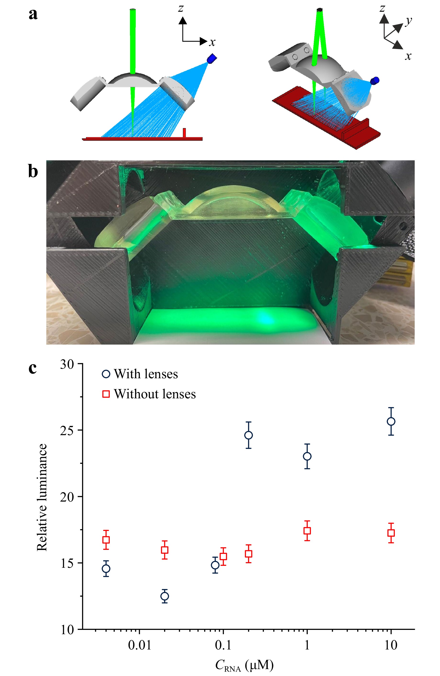
Fig. 7 a Ray tracing of the excitation irradiation and emission collection with the dedicated free-form optics. The sketches show the smartphone case inner set up with excitation beam from one LED, the strip’s emission, the strip holder and the 3D printed lenses (Filters and 3D printed case are omitted for simplification purposes); b Photograph of the assembly interior with the free-form optics; c Assay response toward SARS-CoV-2 RNA as measured with the optical detection device built with (black circles) or without (red squares) three free-form lenses for read-out enhancement.
An RNA oligomer sequence from the RdRp-P1 gene (5’-GGUCCACCUUGUAGUAGGCCACUACG-3’), complementary to the beacon harpin loop, was used for testing of the sensor. Upon increasing concentration of complementary RNA, a fluorescence enhancement resulting from the separation of the fluorescein reporter dye from the quenching unit could be observed.
As shown in Fig. 7c, the results with and without the lenses exhibited a similar background of approx. 40 in relative luminance (Y)58. The signal experienced a prononced increase for concentrations above 0.1 µM of complementary DNA when the 3D-printed case integrates free-form lenses. Interestingly, the percentage measurement error remained similar (approx. 4%), indicating that the free-form polymer lenses enabled lower fluorescence signal detection without drastically increasing the noise of the measurement, as a higher digital gain, i.e., a higher ISO value, would do. From the user’s perspective, the device has an inflection point or OFF–ON value around 0.1 µM, which corresponds to the response of the beacon-based particles. This value is too high to allow direct detection of viral RNA in saliva (500 copies µL–1), but similar to most reported rapid assays59,60, a reasonable number of PCR amplification cycles would allow for screening of infected patients with the developed smartphone based optical device.
-
As optical devices for rapid (bio)chemical analysis advance towards increasingly intricate and miniaturized designs, there is an increasing demand for accessible and cost-effective fabrication methods, especially for high-performance optical elements. The present study demonstrates that stereolithography (SLA) 3D printing offers a practical, user-friendly solution for producing high-quality optical components, thereby extending access beyond the confines of specialized laboratories to non-expert users. A simple and robust post-treatment protocol was developed here to enhance the optical properties of manufactured elements, achieving over 85% transmittance, minimal intrinsic fluorescence, low surface roughness, and refractive indexes approaching that of N-BK7 optical glass. This approach facilitates the rapid prototyping of unconventional and free-form optics, thereby supporting the development of advanced optical systems, including opto-sensors. The integration of SLA-printed free-form optics into a smartphone-based detection device of a rapid SARS-CoV-2 assay demonstrates the efficacy of this method in facilitating the development of miniaturized analytical devices by reducing technical barriers. Beyond analysis and sensing, this work paves the way for scalable, cost-effective solutions in microfluidics, imaging, and photonic device fabrication, rendering optical prototyping accessible to researchers across disciplines, including for example chemists and biologists developing sensors but without specialized expertise in optics.
-
M. A. H. G. thanks BAM for funding (Grant number IE2211). N. Karcioǧlu's assistance with sensor-related experiments is gratefully acknowledged by the authors.
Rapid fabrication of optical elements for sensing applications using a standard SLA printer
- Light: Advanced Manufacturing , Article number: 24 (2026)
- Received: 22 September 2025
- Revised: 09 January 2026
- Accepted: 12 January 2026 Published online: 25 March 2026
doi: https://doi.org/10.37188/lam.2026.024
Abstract: The demand for compact, high-performance optical components has driven the development of increasingly sophisticated and miniaturized optical elements, often requiring complex and costly fabrication methods. In this work, we propose a cost-effective and accessible methodology for the fabrication of lenses and free-form optics using a commercially available stereolithography (SLA) 3D printer. A systematic characterization of six transparent photopolymer resins was conducted in terms of their spectroscopic, optical, and morphological properties, i.e., surface and dimensional properties. The evaluation encompassed parameters such as transmittance, autofluorescence, refractive index, and surface roughness. A straightforward and robust printing and post-treatment protocol was developed, facilitating the fabrication of optical components with over 80% transmittance, minimal intrinsic fluorescence, and a surface quality that is compatible with demanding optical applications. The fabricated components demonstrated excellent dimensional fidelity to digital designs and high reproducibility. To demonstrate the versatility of this approach, aspherical, miniaturized, and free-form lenses were designed and integrated into three fluorescence sensing systems, including oil (strip based) and chlorine (microfluidic based) detection platforms, as well as a smartphone-based SARSCoV-2 biosensor. The integration of customized 3D-printed optics has been shown to improve signal collection and readout performance, thereby highlighting the potential of this approach for broad application by a wide range of user groups in rapid prototyping and use in miniaturized optical systems. This work represents a significant advancement in the field of additive manufacturing, particularly in relation to the development of functional photonic devices. Furthermore, it opens new prospects for sensor applications in biosensing, microfluidics, imaging, and integrated optics.
Research Summary
Additive manufacturing: Low-cost 3D-printed optics for sensing
The fabrication of high-quality miniature lenses and other optical elements has been achieved in a cost-effective manner using standard stereolithography 3D printers. A systematic characterization was conducted on six transparent photopolymer resins in terms of transmission, autofluorescence, refractive index, and surface roughness. A protocol for printing and post-treatment that was both straightforward and rigorous was implemented, resulting in components with over high transmittance, low intrinsic fluorescence, and accurate form. The printed optics demonstrated excellent dimensional fidelity and reproducibility. Aspherical, miniaturized, and free-form lenses were incorporated into oil- and chlorine-detection platforms and a smartphone-based SARS-CoV-2 biosensor, enhancing signal collection and readout. This approach is expected to facilitate more widespread access to rapid prototyping of photonic devices and to encourage advances in compact sensing, microfluidics, and imaging.
Rights and permissions
Open Access This article is licensed under a Creative Commons Attribution 4.0 International License, which permits use, sharing, adaptation, distribution and reproduction in any medium or format, as long as you give appropriate credit to the original author(s) and the source, provide a link to the Creative Commons license, and indicate if changes were made. The images or other third party material in this article are included in the article′s Creative Commons license, unless indicated otherwise in a credit line to the material. If material is not included in the article′s Creative Commons license and your intended use is not permitted by statutory regulation or exceeds the permitted use, you will need to obtain permission directly from the copyright holder. To view a copy of this license, visit http://creativecommons.org/licenses/by/4.0/.

 DownLoad: