


-
Micro-light-emitting diode (micro-LED) displays are emerging as a leading technology for next-generation display platforms, particularly in augmented reality (AR) and virtual reality (VR) applications, owing to their remarkably efficient optical performance, extended operational durability, expansive colour-rendering capability, and robust environmental reliability1–11. Positioned to succeed in OLEDs and conventional LCDs, micro-LEDs are expected to advance both compact and large-format display applications12–14. Recent developments in the micro-LED field have emphasised not only the importance of achieving full-colour capability but also the stringent performance requirements associated with next-generation near-eye display applications such as AR and VR. To simultaneously achieve high colour purity and device miniaturisation, various full-colour strategies have been actively explored, including RGB monolithic growth, colour-conversion layers based on quantum dots or perovskite nanocrystals, and heterogeneous RGB transfer processes. Research in this area has demonstrated that AR and VR systems should achieve high brightness, high external quantum efficiency, fast response times, and precise pixel alignment to deliver high-resolution displays. Such demands underscore the need for pixel-level assembly technologies that can provide both high precision and scalability9,10,15. However, their widespread deployment is hindered by critical technical and economic barriers, including high fabrication costs and the need for highly scalable and precise pixel-level integration methods16–20. Developing a solution to these challenges is crucial for maximising the potential of micro-LED technologies. Numerous strategies have been developed for addressing these issues. However, their widespread adoption is still hindered by critical technical and economic barriers, including high fabrication costs and the need for highly scalable and precise pixel-level integration methods16–20. Developing a solution to these challenges is crucial for maximising the potential of micro-LED technology. Numerous strategies to address these challenges have been investigated. However, established approaches such as mass transfer21–26, laser-assisted transfer27–31, and fluidic self-assembly (FSA)32–35 still face persistent issues, including misplacement, non-uniform assembly, and device degradation, particularly for devices smaller than 5 μm in diameter. These drawbacks are significant obstacles for the integration of micro-LEDs into commercially viable, high-resolution display systems. To illustrate the structural limitations of these established approaches more clearly, we provide a quantitative comparison of representative industrial micro-LED transfer and assembly techniques, including mass-transfer printing, laser-induced transfer, and fluidic self-assembly (Table 1). This comparison reveals that current methodologies struggle to simultaneously achieve the required alignment precision, throughput, and yield for devices with diameters below 5 μm. To overcome these limitations, emerging technologies have focused on nano- to microscale inorganic LEDs with dimensions less than 5 μm36–40. As device dimensions shrink, maintaining the desired electro-optical performance becomes increasingly critical. Preserving the external quantum efficiency (EQE) while simultaneously enabling high-precision assembly and placement is of particular importance.
Method Chip size (μm) Transfer throughput (units h−1) Transfer yield (%) Alignment precision (μm) Cost Ref. Mass transfer printing Ф: ~5 > 6.5 M 99.99 1.5 Medium 21-26 Laser-induced forward transfer Ф: ~50 > 100 M > 90 1.8 High 27-31 Fluidic self-assembly Ф: ~50 > 50 M 99.88 1.25 Medium 32-35 DEP-assisted trapped-assembly 3.96 × 0.72 × 1.2 > 1.22 M 100 No transfer Low Our works Table 1. Comparison of representative micro-LED transfer and assembly techniques.
Over the past decade, our research group has developed miniaturised light-emitting diode (LED) materials and corresponding integration techniques. By enhancing the integration between fluidic deposition strategies and dielectrophoresis (DEP)-assisted assembly, we developed a hybrid assembly platform that offers both economic viability and micron-scale spatial accuracy41–46. In the earlier stages of this research endeavour, we demonstrated the integration of nanorod LEDs into displays. However, we noted that nanorods inherently suffer from optical leakage owing to edge emission and possess a limited multi-quantum well (MQW) volume. To overcome these structural constraints, we adopted an alternative LED structural architecture known as fin-LEDs44. Fin-LEDs, feature a vertically stacked p-GaN/MQW/n-GaN configuration along the short axis, retaining a compact structure comparable to that of nanorods while providing a significant optical advantage by concentrating the MQW layers along the short axis to enhance forward-directed light extraction. Based on these unique features, fin-LEDs are particularly well suited for high-brightness and high-resolution displays. To achieve precise directional assembly, we introduced a face-selective DEP technique that improves the vertical assembly by inducing torque during DEP. This was accomplished by selectively coating low-dielectric materials on the fin-LED sidewalls and integrating an indium tin oxide (ITO) layer on the p-GaN surface to influence the rotational behaviour in the applied field.
Despite recent advances, the precise placement of nanoscale fin-LEDs on the pixel area remains a significant challenge. Fluidic-based techniques, such as inkjet printing and conventional fluidic self-assembly (FSA), suffer from several inherent limitations, including LED sedimentation, nozzle clogging, and insufficient pixel selectivity47,48. These issues collectively diminish the accuracy and scalability. In recent studies on micro- and nanoscale assemblies, researchers have extensively explored the use of external forces and capillary-driven flows to guide the oriented organisation of colloidal nanoscale objects. In this study, a doctor-blade-based assembly strategy was implemented, in which capillary effects and dielectrophoretic (DEP) forces were synergistically utilised to uniformly align fin-LEDs within pixelated regions. Self-assembled monolayers (SAMs) were introduced into the pixel-defining layers to generate surface-energy contrast, enabling selective confinement of the fin-LED ink inside each pixel. This localised ink-trapping structure plays a crucial role in enhancing the directional alignment of fin-LEDs and achieving more uniform placement within individual pixels.
To address these technical challenges, we propose a trapped-assembly (TA) method that combines a doctor-blade-based ink-delivery system with DEP-assisted alignment. This approach enables the precise and directionally controlled placement of fin-LEDs within individual subpixels by confining the ink inside pixel-defined regions during assembly. We systematically optimised key processing parameters, including the viscosity and dielectric properties of the ink solvent, speed and number of doctor-blade passes, vertical distance between the blade and the electrodes, and applied DEP voltage and frequency. By precisely controlling these variables, we effectively confined the ink within each subpixel and achieved a uniform fin-LED distribution while minimising aggregation and misalignment. Our results demonstrate that the TA method, which integrates ink confinement with a DEP-based assembly, enables the highly accurate pixel-level placement of fin-LEDs. This approach provides a scalable and reliable strategy for fabricating next-generation high-resolution displays with uniform light emission and reasonable yields.
-
The fin-LEDs used in this study were fabricated using the same process as reported in our previous study. A schematic of the fabrication procedure is shown in Fig. S1. The fabricated fin-LED structures were confirmed using the scanning electron microscopy (SEM) images shown in Fig. S1f and S1g. Our previous study demonstrated a face-selective assembly technique for fin-LEDs based on DEP forces. Building on this technology, the present study introduces a pixel-defined layer (PDL) to enable precise pixel-level assembly and fabricate an array of 400 pixels. A trapped-assembly approach was implemented by combining doctor-blade-based ink delivery with DEP-assisted assembly. Fig. 1 presents a schematic of the effects of PDL surface properties on the trapped-assembly process. Fig. 1a shows the assembly behaviour without any surface treatment of the PDL. In contrast, Fig. 1b illustrates the trapped-assembly process, in which the PDL treated with octadecyltrichlorosilane (OTS)-based SAMs provides a hydrophobic surface that confines the hydrophobic ink within the pixel cavities, enabling a stable DEP-assisted assembly of the fin-LEDs. Fig. 2 illustrates the evaluation metrics used to quantitatively assess the accuracy and uniformity of fin-LED assembly Fig. 1. Fig. 2a shows the SEM images of various contact configurations of the fin-LEDs, depending on their assembly direction. These include p-GaN contact, n-GaN contact, side contact, and misassembly. As shown in Fig. 2b, the assembly ratio was calculated by subtracting the number of empty pixels that contain no fin-LEDs from a total of 400 pixels. Fig. 2c shows the SEM images used to identify the overlapping fin-LEDs. The assembly ratio was accurately calculated based on the number of nonoverlapping fins. Fig. 2d illustrates the comparison of the number of fin-LEDs per pixel with a ±30% range from the average. Pixels within this range were defined as ‘Active pixels’, while those outside the range were classified as ‘Non-active pixels’. This classification enabled the calculation of a uniform yield. During the trapped-assembly process, the blade was consistently oriented in the direction shown in Fig. S2.
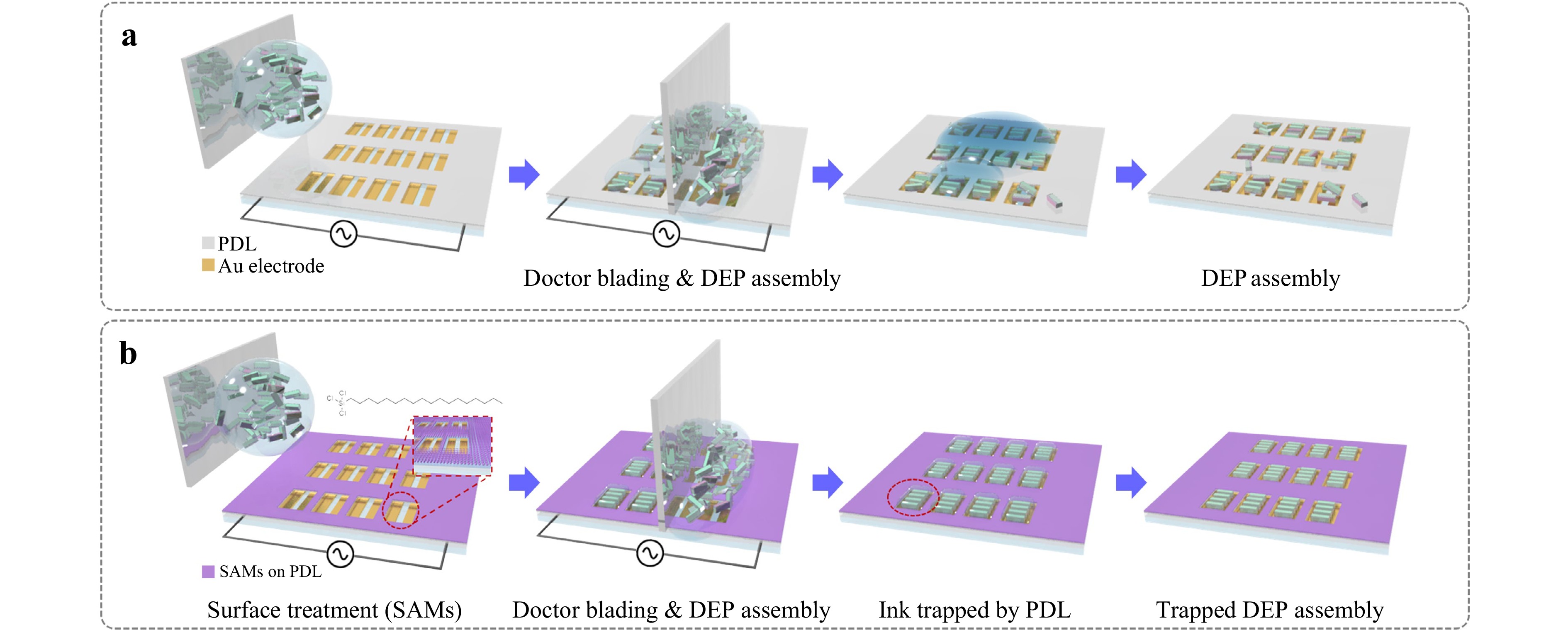
Fig. 1 Schematic of the trapped-assembly process showing the influence of PDL surface properties. a Assembly without PDL surface treatment. b Assembly with hydrophobic PDL obtained via OTS-based SAMs.
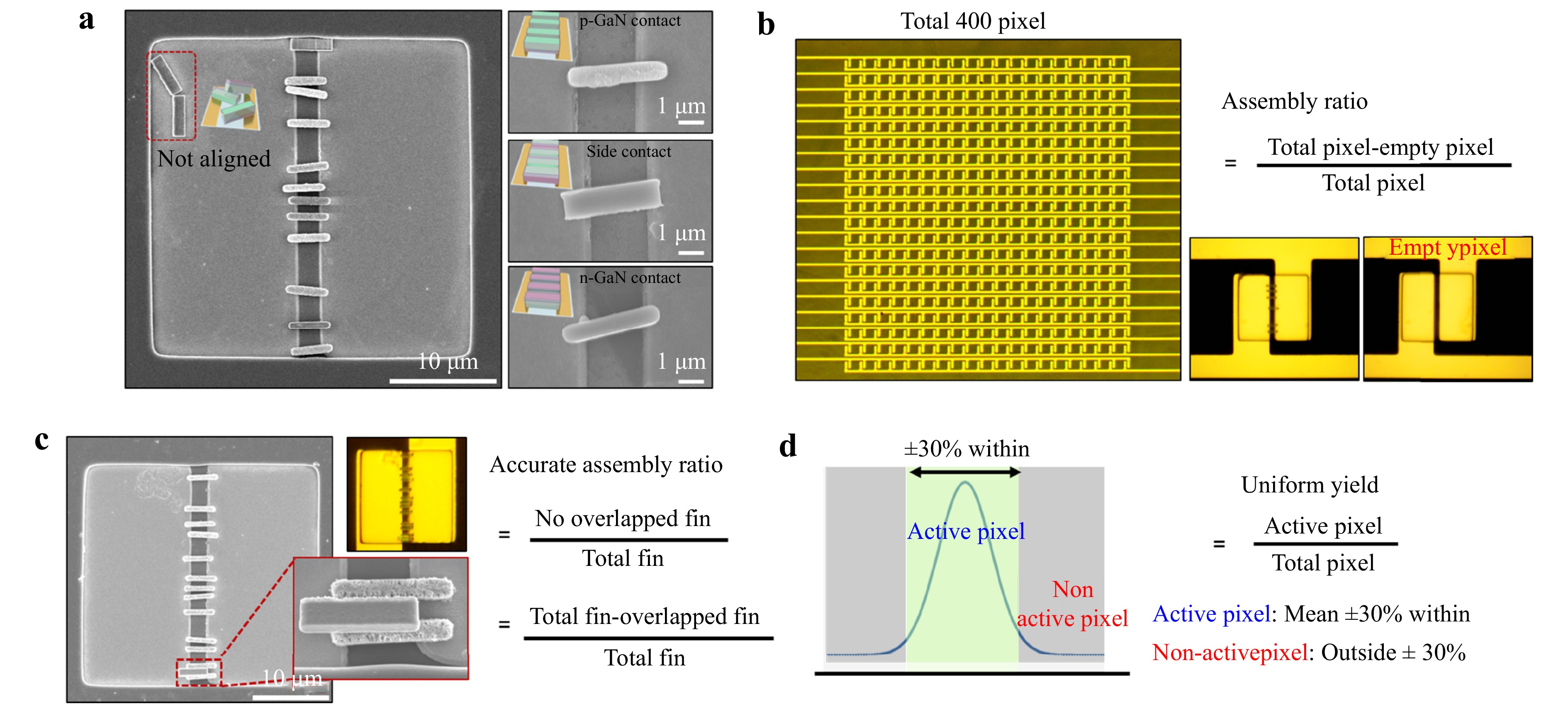
Fig. 2 a A schematic view of the fin-LED structure with the annotated average dimensions and SEM images of p-GaN contact, side contact, n-GaN contact, and non-aligned fin-LEDs on the gold electrode. b Definition of assembly ratio based on the number of pixels containing fin-LEDs out of a total of 400 pixels. c Definition of accurate assembly ratio and d definition of high uniform yield.
Fig. S3 shows the assembly results of fin-LEDs on bare PDL without the OTS SAM treatment using a blade-coating process with different solvents (acetone, gamma-butyrolactone (GBL), ethylene glycol (EG), and polyethylene glycol (PEG)). As shown in the optical microscopy images (Fig. S3a-S3d), the fin-LED ink was not effectively trapped within the pixel cavities under any solvent condition. Furthermore, the SEM images (Fig. S3f, S3g) and assembly ratio calculations (Fig. S3j) revealed that while acetone and GBL exhibited relatively high p-GaN contact assembly ratios exceeding 80%, the number of fin-LEDs assembled per pixel was less than 12, and the uniformity of the assembly was notably reduced. To address this issue, the OTS SAM treatment was introduced to the PDL to facilitate ink trapping within the pixel cavities, which extended the assembly time and enhanced the uniformity of the fin-LED assembly. To investigate the interfacial interactions between the fin-LED ink and the OTS-treated PDL, the assembly behaviour was examined using various solvents, including acetone, GBL, EG, and PEG. The presence of OTS on the PDL surface was confirmed by Fourier-transform infrared (FT-IR) spectroscopy. As shown in Fig. S4, the characteristic C-H stretching peak at 2800–3000 cm−1 indicated the successful formation of the OTS SAMs. Fig. 3 and Table S1 illustrate the influence of the physical properties of the solvents and their interfacial interactions with the OTS-treated PDLs on the assembly behaviour of the fin-LEDs. The four solvents (acetone, GBL, EG, and PEG) exhibited distinct viscosities, conductivities, dielectric constants, and vapour pressures. Owing to these differences, the mobility and assembly stability of fin-LEDs varied significantly, even under identical DEP assembly conditions. The effects of the interfacial interactions between the OTS-treated PDL and the four solvents with different physical properties (acetone, GBL, EG, and PEG) on the assembly behaviour of the fin-LEDs are summarised in Fig. 3 and Table S1. These solvents exhibit notable differences in viscosities, electrical conductivities, dielectric constants, and vapour pressures. Consequently, even under identical DEP conditions, the mobility and assembly stability of the fin-LEDs varied significantly depending on the solvent used. In particular, acetone, which has the lowest viscosity and highest vapour pressure among the solvents, showed poor solvent trapping within the pixel regions, as observed in the optical microscopy and SEM images in Fig. 3a, e, respectively. In addition, the SEM image and data in Fig. 3k revealed that acetone had the lowest p-GaN contact ratio of 29.6%, indicating poor assembly quality. As shown in the optical microscopy and SEM images in Fig. 3b, f, GBL provided an improved fin-LED assembly ratio compared to acetone. In addition, the p-GaN contact ratio increased to 69.3%, as shown in Fig. 3k. EG, which had a slightly higher viscosity and lower vapour pressure than GBL, exhibited improved solvent trapping in the optical microscopy and SEM images in Fig. 3c, g, respectively, and the p-GaN contact ratio increased to 77.2%. As shown in the optical microscopy and SEM images in Fig. 3d, h, PEG, the solvent with the highest viscosity and lowest vapour pressure, demonstrated effective trapping. It also afforded the highest p-GaN contact ratio of 96%. However, as the viscosity increased and the vapour pressure decreased, the number of fin-LEDs assembled per pixel decreased significantly, as shown in Fig. 3j. Fig. 3i compares the contact angles of each solvent on the bare and OTS-treated PDL surfaces, showing a marked increase in hydrophobicity after the OTS treatment for all solvents. Evidently, this improved hydrophobicity contributed to enhanced ink confinement within the pixel cavities. As shown in Fig. 3i, the contact angle of the OTS-treated PDL was measured to be 106°, confirming successful hydrophobic surface modification. In all solvents, the OTS treatment increased the contact angle, thereby enhancing the hydrophobicity and improving ink confinement within the pixel cavities.
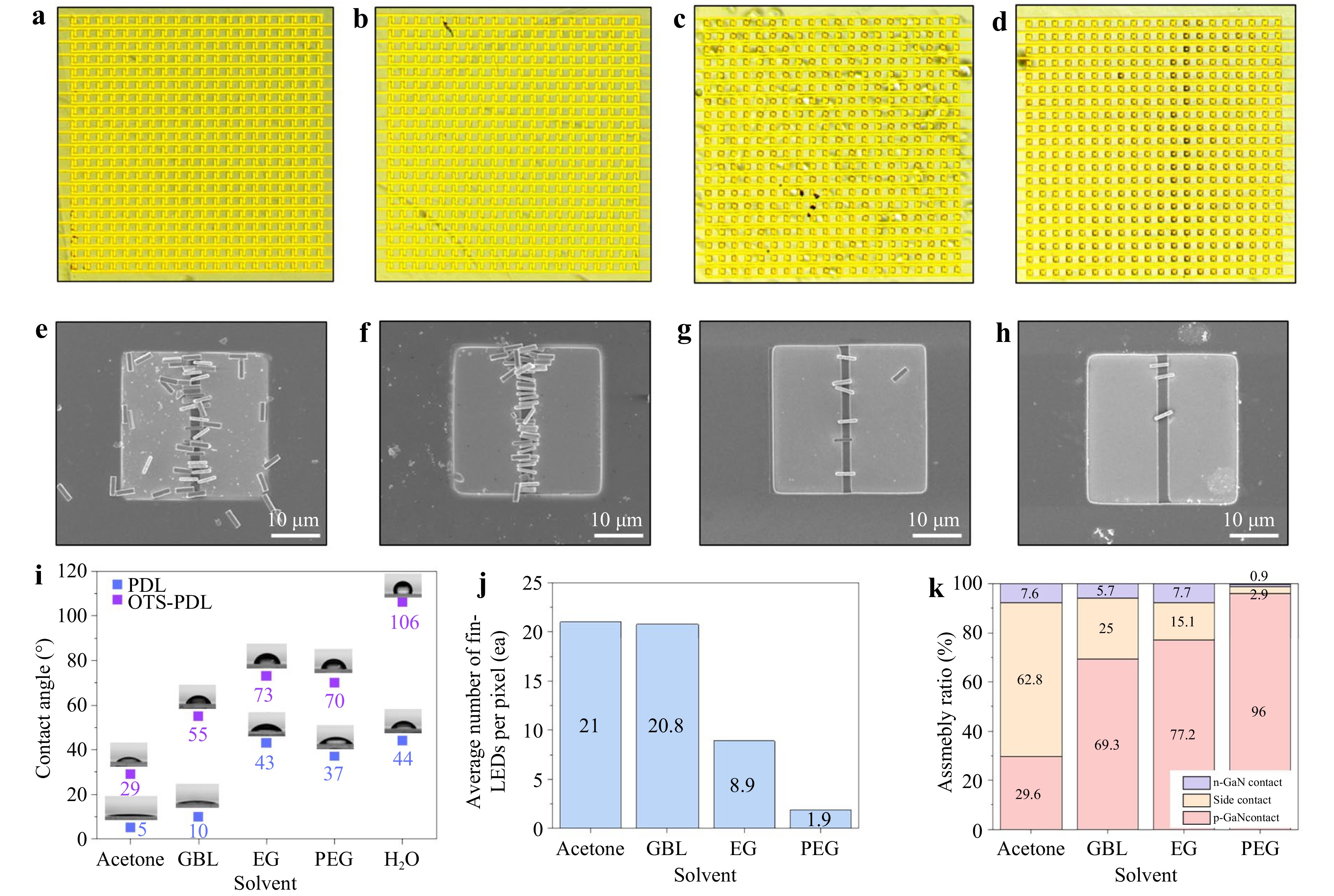
Fig. 3 Optical microscope images of assembled fin-LEDs using different solvents: a acetone, b GBL, c ethylene glycol, and d polyethylene glycol. SEM images of fin-LEDs assembled using different solvents: e acetone, f GBL, g ethylene glycol, and h polyethylene glycol. i Contact angles and images (inset) of bare PDL and OTS-treated PDL for each solvent. j Average number of fin-LEDs per pixel assembled using each solvent-based fin-LED ink. k Assembly ratio of fin-LEDs using various ink solvents.
To address this limitation, a bi-solvent system combining acetone and PEG was introduced. The aim of this approach was to maintain effective solvent trapping while enhancing both the p-GaN contact ratio and the number of assembled fin-LEDs within each pixel (Fig. 4). As shown in Fig. 4, PEG and acetone were mixed at three different volume ratios: 25, 50, and 75 vol%. The optical images of the assembled fin-LEDs presented in Fig. 4a-c reveal that the number of assembled LEDs within each pixel gradually decreased with increasing PEG concentration. This is attributed to the higher viscosity of PEG, which limited the mobility of the fin-LEDs under DEP. The results of the quantitative analysis presented in Fig. 4e show that the average number of fin-LEDs per pixel was highest at 25 vol% PEG, with an average of 9.6 devices and a relatively low standard deviation. As the PEG content increased to 50 and 75 vol%, the average decreased significantly, indicating insufficient DEP-induced assembly. Additionally, as shown in Fig. 4d, the assembly ratio reached 100% at 25 vol% PEG, confirming that solvent trapping was effective under these conditions. The uniform yield also reached its highest value of 57.3%, suggesting that the pixel-level consistency was improved. Importantly, the overlap between the fin-LEDs was significantly reduced when the PEG–acetone mixture was used. As shown in Fig. 4f, the percentage of overlapping fin-LEDs decreased to 10% at 25 vol% PEG, whereas 90% of the devices exhibited an accurate, non-overlapping assembly. This represents a major improvement compared to the overlap ratio observed under the single-solvent conditions depicted in Fig. 3. Overall, the 25 vol% PEG and acetone mixture provided a favourable balance between fluidic confinement and fin-LED mobility, which enabled a high assembly ratio, uniform distribution, and minimal overlap within the pixel array.
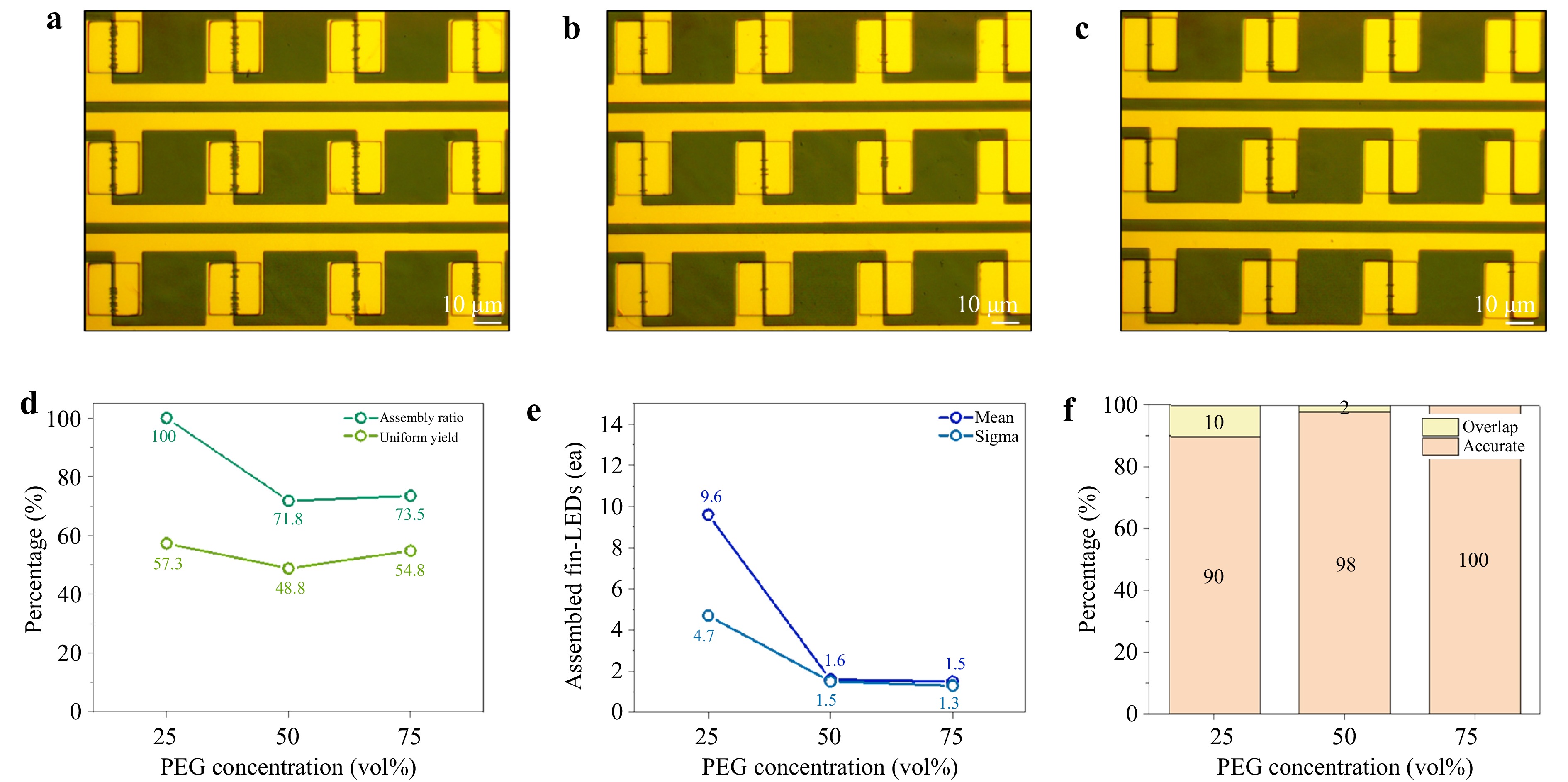
Fig. 4 Optical microscope images of assembled fin-LEDs using PEG/acetone mixed solvents with different PEG concentrations: a 25 vol%, b 50 vol%, and c 75 vol%. d Assembly ratio and uniform yield as a function of PEG concentration. e Mean and standard deviation (sigma) of the number of assembled fin-LEDs per pixel. f Ratio of overlapped fins and accurately assembled fin-LEDs for each PEG concentration.
Based on the optimised PEG:acetone = 25:75 (vol%) bi-solvent system, the assembly behaviour was investigated as a function of the applied voltage and frequency, as shown in Fig. 5. As shown in Fig. 5a, when the voltage was increased from 10 Vpp to 40 Vpp at a fixed frequency of 50 kHz, the assembly ratio improved from 82.5% to 100%, and the uniform assembly yield increased from 50% to a maximum of 75%. In addition, as shown in Fig. 5b, the average number of assembled fin-LEDs per pixel increased significantly from 1.3 at 10 Vpp to 20.4 at 40 Vpp. However, as shown in Fig. 5c, the number of overlapping fin-LEDs increased with increasing voltage. This indicates that excessive assembly at high voltages leads to overlap. Therefore, 20 Vpp was selected as the optimal condition because it yielded a sufficient number of assembled fin-LEDs per pixel with a low overlap rate. Based on this, the assembly characteristics were further analysed by varying the frequency from 10 to 200 kHz. As shown in Fig. 5d, the assembly ratio remained relatively stable, with values greater than 93% under all conditions. As evident from Fig. 5e, the average number of assembled fin-LEDs per pixel peaked at 9.3 at 100 kHz, while relatively fewer fin-LEDs were assembled at other frequencies. Fig. 5f shows that the overlap rate remained low (8%–9%) across most frequency conditions, whereas the accurate assembly rate was consistently above 90%. These results indicate that the frequency does not significantly affect assembly uniformity or accuracy. Therefore, 100 kHz and 20 Vpp were identified as the optimal conditions to achieve a trapped assembly.
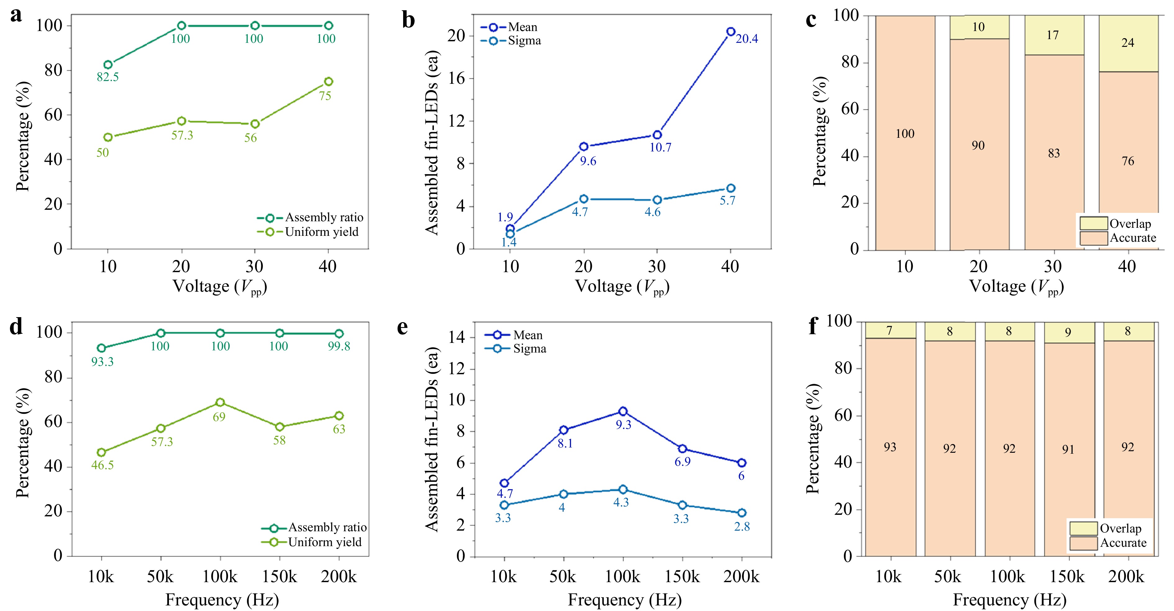
Fig. 5 a Assembly ratio and uniform yield as a function of applied voltage. b Mean and standard deviation (sigma) of the number of assembled fin-LEDs per pixel at different voltages. c Ratio of overlapped fin-LEDs and accurately assembled fins for each voltage condition. d Assembly ratio and uniform yield as a function of applied frequency. e Mean and standard deviation (sigma) of the number of assembled fin-LEDs per pixel at different frequencies. f Ratio of overlapped fins and accurately assembled fin-LEDs for each frequency condition with optical microscope images (inset).
Fig. 6a presents the effect of blade height and blade moving speed on the assembly behaviour of fin-LEDs under the conditions of a PEG:acetone = 25:75 (vol%) mixed solvent with an electrical input of 20 Vpp and 100 kHz. To investigate the effect of blade height, the distance was varied from 50 to 500 μm. As can be observed in Fig. 6b, the assembly ratio increased from 96.7% to 99.8% with increasing blade height, whereas the uniform assembly yield improved from 49.5% to 61%. This trend can be attributed to a reduction in the physical pressure applied by the blade on the droplet, which limited spreading and provided a more stable DEP-based assembly. Fig. 6c shows that the average number of fin-LEDs assembled per pixel also increased with blade height, reaching a maximum of 6.2 at 500 μm. However, as seen in Fig. 6d, the overlap rate also rose with increasing height, with a 9% overlap observed at 500 μm, indicating a corresponding decrease in accurate assembly. Next, the effect of blade speed was examined under conditions ranging from 0.05 to 4 mm·s−1. As shown in Fig. 6e, the highest uniform assembly yield of 71% was obtained at a speed of 1 mm·s−1. At 0.5 mm·s−1, the yield was 63%, while at 4 mm·s−1 it dropped to 47%, which indicated that assembly uniformity clearly depended on blade speed. In Fig. 6f, an average of 11.1 fin-LEDs were assembled per pixel at 0.05 mm·s−1, but the number decreased as the speed increased. This is likely due to the longer DEP exposure time at lower speeds, which allows more fin-LEDs to be attracted. However, as shown in Fig. 6g, the overlap rate was the highest at 12% under 0.05 mm·s−1. This suggests an excessive assembly of LED due to overlap-related defects. In contrast, the overlap rate at 1 mm·s−1 was lower at 7 while the accurate assembly rate was maintained at 93%, and accordingly, this was determined to be the optimal blade speed. Therefore, a blade height of 500 μm and a blade speed of 1 mm·s−1 were identified as the critical operating conditions that simultaneously maximise assembly ratio and uniform yield while ensuring overall process stability and reproducibility. These findings demonstrate that both the blade height and blade speed are decisive parameters that directly influence the number of assembled fin-LEDs, assembly uniformity, and overlap rate. Consequently, the precise optimisation of each parameter is essential for achieving high-performance DEP-based assemblies. Based on the optimised assembly conditions described above, the effect of the dispersion concentration was evaluated by separating the fin-LEDs from a quarter section of a 4-inch GaN-on-sapphire wafer and dispersing them in 6 mL of the optimised 25 vol% PEG solvent to prepare a stock solution. Based on this stock solution, inks with three different relative concentrations (×1, ×2, and ×3) were prepared, quantified using UV-Vis spectroscopy, and subsequently used to examine the assembly performance. The assembly results shown in Fig. S5 revealed that higher concentrations led to an increased uniform yield; however, the average number of assembled fin-LEDs per pixel also increased to 13.7, resulting in a higher overlap ratio. Conversely, lower concentrations reduced the overlap but decreased both the uniform yield and the number of assembled fin-LEDs. Considering these trade-offs, we determined that the ×2 concentration provided the best balance between assembly consistency and minimal overlap and therefore used this concentration as the optimal condition for subsequent experiments.
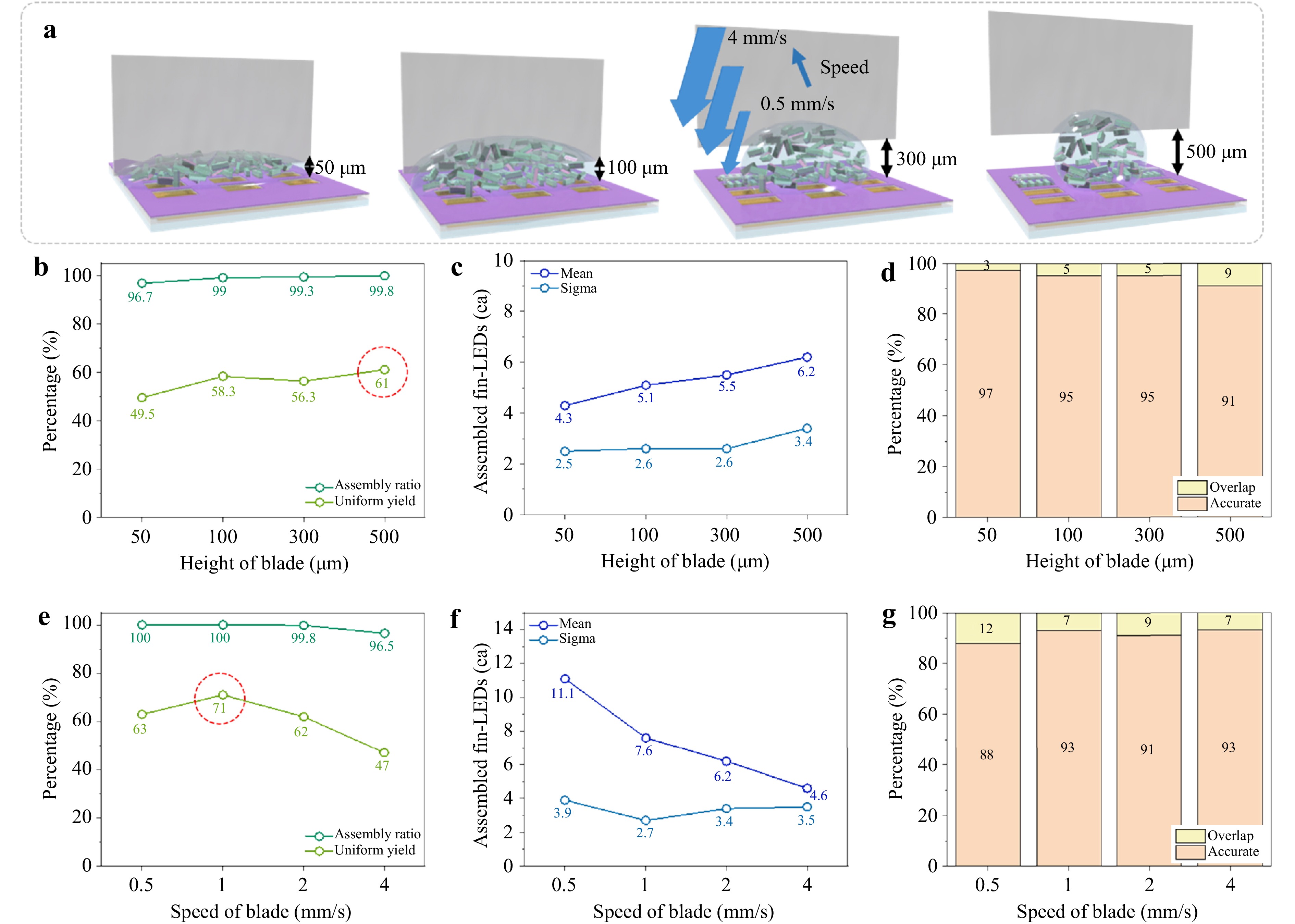
Fig. 6 a Schematic of the height of blade and speed of blade during assembly process. b Assembly ratio and uniform yield as a function of blade height. c Mean and standard deviation (sigma) of the number of assembled fin-LEDs per pixel at different blade heights. d Ratio of overlapped fins and accurately assembled fin-LEDs for each blade height condition. e Assembly ratio and uniform yield as a function of blade speed. f Mean and standard deviation (sigma) of the number of assembled fin-LEDs per pixel at different blade speeds. g Ratio of overlapped fin-LEDs and accurately assembled fins for each blade speed condition.
Fig. 7 illustrates the effect of blade coating repetition on the assembly characteristics of fin-LEDs under identical DEP assembly conditions (PEG:acetone = 25:75 vol%, 20 Vpp, 50 kHz) using a blade speed of 1 mm·s−1 and a blade height of 500 μm. As the number of blades passing over the same position increased, the probability of guiding the fin-LEDs toward the electrode was expected to improve because of the repeated exposure to the electric field. To evaluate this, single-, double-, and triple-pass blade coatings were applied and compared, as shown in the optical microscopy images in Figs. 7a-c. As shown in Fig. 7d, the uniform assembly yield increased progressively with the number of blade passes: 57.8% for a single-pass, 67.3% for a double-pass, and 84.8% for a triple-pass. The overall assembly ratio remained above 99% across all conditions, with the triple-pass method achieving 100% assembly. These results suggest that repeated blade coating enhances the number of assembled pixels and improves assembly uniformity. As shown in Fig. 7e, the average number of assembled fin-LEDs per pixel also increased with additional passes—from 8.1 for the single-pass to 12.7 for the double-pass and 16.7 for the triple-pass. Meanwhile, the standard deviation remained below four in all cases, indicating consistent assembly results. Fig. 7f shows that the overlap ratio increased slightly with more blade passes, measuring 10% for both the single-pass and double-pass and 12% for the triple-pass. Nevertheless, the assembly ratio remained above 88% under all conditions (Fig. 7g). This suggests that, while repeated passes improve the assembly quantity and uniformity, they may introduce a slight increase in overlap owing to over-assembly. Overall, increasing the number of blade passes is an effective approach for enhancing the assembly efficiency and uniformity of fin-LEDs. Among the tested conditions, the triple-pass blade coating provided the highest assembly yield and uniformity while maintaining a high degree of accuracy; thus, it was the optimal process condition. In addition, when the electroluminescent (EL) devices were fabricated under each blade-pass condition, the triple-pass process resulted in more uniform emission across the pixels compared to the single-pass process, as shown in Fig. 7c. This is attributed to the higher number of assembled fin-LEDs per pixel in the triple-pass condition, as also seen when contrasted with Fig. 7a.
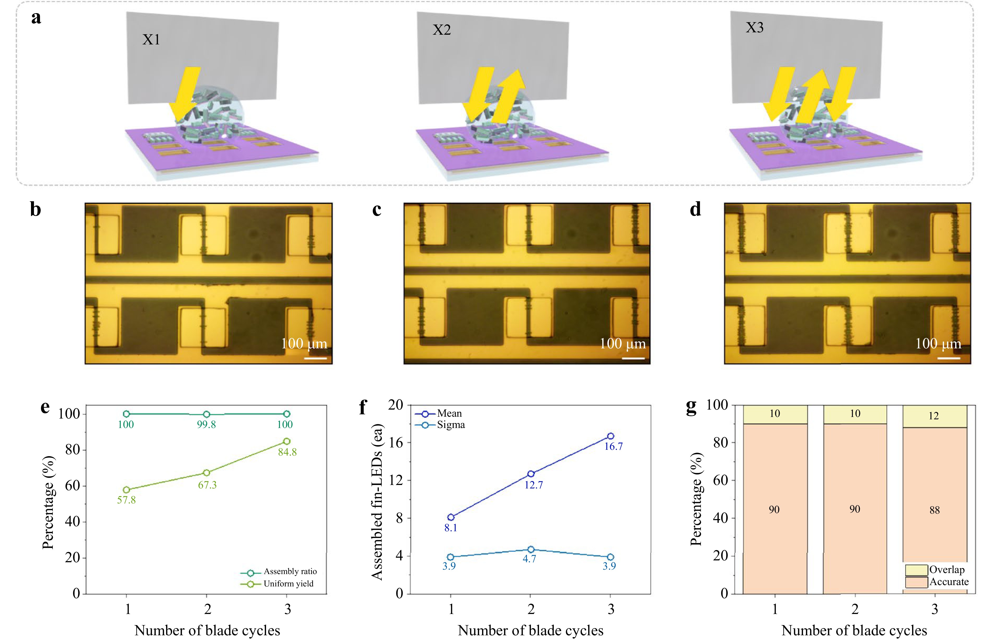
Fig. 7 a Schematic of the number of blade cycles during the assembly process. Optical microscope images after b one cycle, c two cycles, and d three cycles. e Assembly ratio and uniform yield as a function of the number of blade cycles. f Mean and standard deviation (sigma) of the number of assembled fin-LEDs per pixel for different blade cycles. g Ratio of overlapped fins and accurately assembled fin-LEDs for each blade cycle condition.
Fig. 8 presents the comprehensive results of the fin-LED assembly achieved under the optimised process conditions. In this study, a mixed solvent of PEG and acetone at a ratio of 25:75 (vol%) was used, and the electric field conditions were set to 100 kHz and 20 Vpp. The blade coating process was carried out at a speed of 1 mm·s−1, with a blade height of 500 μm and triple-pass coating. These conditions were selected as the optimal conditions based on previous parametric experiments in which the highest assembly uniformity and accuracy were demonstrated. Fig. 8a shows an optical microscopy image of the entire array assembled under the optimised conditions, confirming that the fin-LEDs were successfully assembled in all pixels. The assembled fin-LEDs were then used to fabricate EL devices. Fig. 8b shows a magnified image of a single pixel, clearly showing the fin-LEDs trapped and assembled within the electrodes. Fig. 8c presents an EL image of the assembled array, wherein most of the pixels exhibit uniform emission, indicating excellent assembly uniformity and reliable electrical contact.
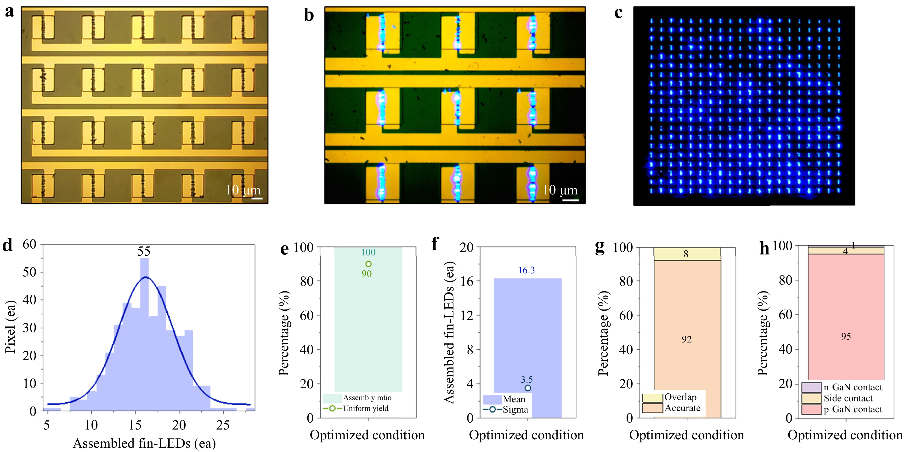
Fig. 8 a Optical microscope image and b high-magnification optical microscope image showing the fin-LED assembly under the optimized conditions: 25 vol% PEG, 20 Vpp, 100 kHz, blade speed of 1 mm·s−1, blade height of 500 μm, and three cycles. c EL image of the fin-LED device under the optimized conditions. d Distribution of fin-LED counts per pixel. e Assembly ratio and uniform yield. f Mean and standard deviation (sigma) of the number of assembled fin-LEDs per pixel. g Ratio of overlapped fins and accurately assembled fin-LEDs under the optimized conditions.
Fig. 8d shows a histogram of the number of assembled fin-LEDs per pixel. Out of 400 pixels, 360 exhibited fin-LED counts within the range of 12–20, corresponding to a uniform assembly yield of 90%. Fig. 8e shows an overall assembly ratio of 100% and uniform assembly yield of 90%. Fig. 8f shows that the average number of assembled fin-LEDs per pixel was 16.3, with a standard deviation of 3.5, demonstrating a consistent assembly performance. As shown in Fig. 8g, the overlap ratio was 8%, and the accurate assembly ratio reached 92%, indicating that a high assembly density was maintained without significant overlap. Finally, Fig. 8h shows that 95% of the assembled fin-LEDs were in contact with the p-GaN surface. This confirms that the solvent composition plays a critical role in determining the assembly orientation. These results demonstrate that precise control of the solvent composition, electric field conditions, and blade parameters enables the implementation of a highly accurate and uniform DEP-based assembly process for fin-LEDs. To accurately evaluate the emission characteristics of the fin-LEDs, we first fabricated a test cell with an active area of 1 mm × 1 mm, an electrode width of 10 μm, and an electrode spacing of 2 μm, as shown in Fig. S6. This test structure was designed to reliably probe the intrinsic emission behaviour of fin LEDs, which cannot be directly assessed in a highly integrated array geometry. The EL measurements from the test cell exhibited a maximum EQE of approximately 8.2% at a current density of 0.011 A cm−2 and a luminance of 6121 cd m−2 at 0.25 A cm−2, confirming the high performance of the individual fin-LED emitters. The EL characteristics of the array cell fabricated under the optimised conditions were also evaluated. The array cell exhibited a maximum EQE of 3.26% at a current density of 0.0157 A cm−2 and a luminance of 1584 cd m−2 at 0.28 A cm−2 (Fig. S6). Evidently, the lower luminance observed in the array cell compared to the test cell is attributable to the relatively large pixel pitch of 70 μm, which increases the ratio of non-emissive to emissive areas and thereby limits the effective emission area and light-extraction efficiency. In addition, consistent EL characteristics were obtained for multiple test cells fabricated using the same DEP-based alignment and assembly process, demonstrating the high reproducibility of the optimised process and its applicability to various device configurations. These results indicate that further optimisation of the device structure and fabrication process can enhance the performance of the array configuration, suggesting a strong potential for future high-resolution display applications.
-
In this study, we propose a high-precision assembly technique to implement high-resolution nano- to microscale displays based on a trapped-assembly method that combines a doctor-blade-based ink-delivery system with DEP-induced assembly. This method effectively confines the ink within individual pixels to minimise the diffusion and aggregation of fin-LEDs during the assembly process and enhances the overall stability. To this end, OTS SAMs were applied to the PDL to induce ink trapping and establish trapped-assembly conditions. The key process parameters, including the viscosity and dielectric properties of the ink solvent, speed and number of blade passes, gap between the blade and the substrate, and applied DEP voltage and frequency, were systematically optimised. The optimal conditions were thereupon identified as a PEG:acetone bi-solvent at 25:75 vol%, a DEP voltage of 20 Vpp, a frequency of 100 kHz, a blade height of 500 μm, a blade speed of 1 mm·s−1, and triple-pass coating. Under these conditions, successful fin-LED assembly was achieved for all 400 pixels, with 90% of the pixels containing 12–20 fin-LEDs per pixel. The average number of assembled fin-LEDs was 16.3 with a standard deviation of 3.5. The overlap ratio was 8%, and 92% of the fin-LEDs were accurately assembled. In addition, 95% of the fin-LEDs were in contact with the p-GaN surface, indicating effective orientation control. The EL devices fabricated using the assembled fin-LEDs exhibited bright and uniform emissions across the entire pixel array, which confirmed not only the excellent assembly quality but also the high electrical reliability.
In conclusion, the DEP-based trapped-assembly method developed in this study provides a reliable and scalable process strategy for achieving a high-yield, high-accuracy pixel-level assembly of fin-LEDs. By effectively overcoming the limitations of conventional fluidic assembly techniques, this approach demonstrates clear potential for extension to large-area and flexible substrates and further shows applicability to display systems employing colour-conversion layers. Therefore, the proposed method is expected to serve as a promising solution for practical integration of nanoscale and microscale LEDs into next-generation high-resolution display technologies.
-
The blue epitaxial wafer used in this study was purchased from SEMITEK Co. (Taiwan) and consisted of a 50 nm p-GaN layer, a 150 nm InGaN/GaN multiple quantum well (MQW) structure, and a 2.0 μm n-GaN layer, and a 1.5 μm u-GaN layer. To form the current-spreading layer, a 150 nm indium tin oxide (ITO) film was deposited using RF sputtering. Subsequently, a bilayer hard mask consisting of 200 nm aluminium and 900 nm SiO2 layers was sequentially deposited using an electron beam evaporator and plasma-enhanced chemical vapour deposition (PECVD), respectively. Nanoimprint lithography was used to define the fin-LED structures. For this process, a spin-on-glass (SOG) material (FOX-16, DOW Corning Co.) was spin-coated onto a PDMS mould (Sylgard® 184, Dow Corning Co.), which was then laminated onto the masked GaN wafer under uniform pressure to transfer the fin-like nanopattern onto the Al layer. The hard mask was etched by sequentially removing the Al and SiO2 layers using chlorine-based inductively coupled plasma (ICP) and fluorine-based reactive-ion etching (RIE), respectively. The patterned GaN structure was subsequently etched using Cl2-based ICP to define the fin-LED structures.
To mitigate plasma-induced damage during dry etching, the sample was treated with tetramethylammonium hydroxide (TMAH, 25 wt% in water, Sigma-Aldrich) at 80 °C for five minutes. To suppress excessive porosity during subsequent electrochemical etching (ECE), a 50 nm-thick SiO2 layer was deposited via PECVD. After partial removal of the n-GaN bottom region, the ECE process was carried out in a 0.3 M oxalic acid solution for 5 min to induce porosity and enable detachment of the fin-LEDs from the substrate. Following the ECE process, the SiO2 protective layer was eliminated using a buffer oxide etchant (BOE), and a passivation layer was applied. The detached fin-LEDs were released from the wafer after 5 min of sonication in gamma-butyrolactone (GBL), followed by solvent exchange and purification using acetone.
-
As shown in Fig. S7, the first step of the fin-LED assembly process involved the patterning of the electrodes using a photolithography process with a negative photoresist to achieve precise assembly and placement within each pixel. Subsequently, 10 nm of Cr and 200 nm of Au layers were deposited using an e-beam evaporator. A lift-off process with acetone was then performed to form electrode pairs with a width of 15 μm and a gap of 2 μm. To concentrate the electric field within each pixel, a PDL was formed on top of the electrodes using SU8 2002 photoresist and then patterned into 400 square pixels with dimensions of 30 μm × 30 μm and a pitch of 70 μm.
To implement the trapped-assembly method, a self-assembled monolayer (SAM) of OTS was selectively formed on the surface of SU8-based PDL to induce hydrophobicity. A positive photoresist (AZ 5214) was first coated and then selectively exposed to the same mask, leaving only the PR inside the pixel regions. After the O2 plasma treatment, hydroxyl groups were introduced on the SU8 surface. The substrate was then immersed in a solution of 10 μL of OTS in 20 mL of anhydrous hexane for 1 h to form SAMs. Finally, the PR inside the pixel was removed using acetone, resulting in a selective OTS coating on the SU8 PDL.
The assembly process was conducted using the trapped-assembly approach. A 3 μL droplet of fin-LED ink dispersion was placed outside the active electrode area and then dragged across the pixelated region using a doctor blade. The ink was effectively confined within the pixel cavities, while the fin-LEDs were directed and assembled into the pixels under the influence of DEP. This process relied on three cooperative mechanisms: surface energy control achieved through the OTS treatment, physical trapping driven by blade motion, and electrical assembly induced by DEP, all of which contribute to the achievement of a highly oriented and precise assembly. To further investigate the assembly characteristics, various parameters, including ink-solvent properties, DEP voltage and frequency, blade speed and stroke count, and vertical gap between the blade and electrodes, were systematically varied and analysed.
A quantitative evaluation was performed by analysing all 400 pixels based on three metrics: the assembly ratio, uniform yield, and overlapped fin-LED yield. Pixels containing at least one fin-LED were considered active and used to calculate the assembly ratio. Pixels with a number of fin-LEDs within ±30% of the average were categorised as uniform, and the corresponding uniform yield was determined. Additionally, the number of pixels containing overlapping fin-LEDs was counted to calculate the yield of the overlapped fin-LEDs and comprehensively assess the overall assembly quality.
-
Electroluminescent devices were fabricated using fin-LEDs assembled within 400 pixels. First, a 40 nm SiO2 layer was deposited via electron-beam evaporation to provide mechanical anchoring. An insulating layer was then formed using SU-8 photoresist, exposing the p-pad electrodes. Dry etching was performed using RIE to expose the n-GaN faces of the fin-LEDs. Finally, a 500 nm transparent conductive oxide layer composed of aluminium-doped zinc oxide (AZO) was deposited across the entire surface via RF sputtering to complete the device fabrication.
-
The structural characteristics of the fabricated fin-LEDs were examined using scanning electron microscopy (SEM, JSM-7610F; JEOL Ltd., Japan). X-ray diffraction (XRD, Ultima IV, Rigaku) and Raman spectroscopy (λ = 532 nm, Nd:YAG laser) were used to evaluate the crystallinity and overall structural integrity of the fin LED array. Transmission electron microscopy (TEM, JEM-2100F, JEOL Ltd., 200 kV) was used to analyse the microstructures of the individual fin-LEDs. The quality of the fin-LED assembly was quantitatively assessed by a statistical analysis of the optical and SEM imaging data. To characterise optical properties, photoluminescence (PL) was measured using a Ti:Sapphire laser (λ = 355 nm). The electroluminescence (EL) behaviour and current–voltage–luminance (IVL) responses of the fabricated devices were recorded using a CS-2000 spectroradiometer (Konica Minolta) and a Keithley 2001 source meter (Keithley Instruments Inc.).
-
This work was supported by a National Research Foundation of Korea (NRF) grant funded by the Korea government (MSIT) (RS-2021-NR059326) and the Nano & Material Technology Development Program through the National Research Foundation of Korea (NRF) funded by Ministry of Science and ICT(RS-2023-00281346).
Dielectrophoretic-assisted trapped-assembly for fin-LED display
- Light: Advanced Manufacturing , Article number: 26 (2026)
- Received: 30 August 2025
- Revised: 15 January 2026
- Accepted: 16 January 2026 Published online: 15 April 2026
doi: https://doi.org/10.37188/lam.2026.026
Abstract: We propose a high-precision assembly technique for realizing high-resolution nano- to microscale displays using a trapped-assembly approach that integrates a doctor-blade-based ink-delivery system with dielectrophoresis (DEP)-induced assembly. Octadecyltrichlorosilane (OTS) self-assembled monolayers (SAMs) were coated onto the pixel-defined layer (PDL) to promote ink trapping and confine fin-LEDs within individual pixels during assembly. Key process parameters—including the viscosity and dielectric properties of the ink solvent, speed and number of blade passes, blade-to-substrate gap, and applied DEP voltage and frequency—were systematically optimised, as these parameters affect solvent confinement of the solvent and fin-LED assembly behavior. Under optimised conditions, achieved through precise control of solvent polarity, DEP force and torque, and doctor-blading parameters, all 400 pixels were successfully assembled. Statistical analysis revealed that 90% of the pixels contained 12-20 fin-LEDs, with an average of 16.3 fin-LEDs per pixel and a standard deviation of 3.5. The overlap ratio was limited to 8%, and 92% of the fin-LEDs were accurately assembled, of which 95% established contact with the p-GaN surface. Electroluminescent devices fabricated using the assembled fin-LEDs exhibited bright and uniform emission across the entire pixel array, confirming their excellent assembly quality and high electrical reliability. The DEP-based trapped-assembly method provides a reliable and scalable strategy for the practical integration of nano- to microscale LEDs in next-generation high-resolution display technologies.
Research Summary
Trapped assembly improves fin-LED assembly for displays
Assembling high-aspect-ratio fin-shaped sub-micro-LEDs with dimensions below 5 µm with high yield and uniformity remains a major challenge for advanced display manufacturing. Conventional dielectrophoretic assembly often suffers from lateral sliding and rotational instability, leading to non-uniform pixel emission. In this work, a trapped-assembly framework is introduced by incorporating dielectric-guided barrier lines that reshape the local electric-field distribution. This configuration produces a central focusing force that stabilizes fin-LEDs during assembly and promotes reliable vertical alignment. Systematic optical and electrical analyses reveal enhanced alignment yield and improved electroluminescence uniformity at the pixel level. The proposed trapped-assembly approach offers a controllable and scalable solution for integrating fin-LEDs into high-density display architectures.
Rights and permissions
Open Access This article is licensed under a Creative Commons Attribution 4.0 International License, which permits use, sharing, adaptation, distribution and reproduction in any medium or format, as long as you give appropriate credit to the original author(s) and the source, provide a link to the Creative Commons license, and indicate if changes were made. The images or other third party material in this article are included in the article′s Creative Commons license, unless indicated otherwise in a credit line to the material. If material is not included in the article′s Creative Commons license and your intended use is not permitted by statutory regulation or exceeds the permitted use, you will need to obtain permission directly from the copyright holder. To view a copy of this license, visit http://creativecommons.org/licenses/by/4.0/.

 DownLoad: