


-
Surface-enhanced Raman scattering (SERS) is widely used for trace detection and compositional analysis of biochemical samples1–8 because it is non-destructive9, non-contact10,11, and highly sensitive12. However, because of its low intensity of Raman scattering, observing Raman scattering using conventional methods is challenging13. Chemical enhancement (CM) and electromagnetic enhancement (EM) are the two widely used SERS mechanisms14,15. In the chemical mechanism, photoinduced charge transfer strongly increases molecular polarisability and amplifies the Raman signal. In the electromagnetic mechanism, incident light excites localised surface plasmons on metallic nanostructures and increases the intensity of the local electric fields. SERS substrates use electromagnetic hot spots provided by micro-nanostructures to enhance Raman scattering signals16–18. Thus, building multidimensionally ordered hotspots with high density and intensity on SERS substrates is key to maximising electromagnetic enhancement.
SERS substrates based on noble-metal nanoparticles or other micro/nanostructures have been widely studied. In recent years, the design of SERS substrates has transitioned from traditional single micro/nanostructure (micropores19,20, micropillars21,22, microlens23, and micropyramids24,25) to hierarchical micro/nanocomposite structures. Jin et al. fabricated a SERS substrate with micropyramid arrays and bionic compound eye structures using nanosphere lithography and anisotropic wet etching. The antireflective properties of these arrays significantly improved the intensity of the Raman signal26. Yan et al. utilised the imprint-transfer technique to fabricate slot-under-slot nanoarrays. They improved the enhancement performance of SERS substrates and significantly expanded their detection range27. Gao et al. fabricated wrinkled nanocone-flexible SERS substrates on transparent PET films by colloidal photolithography and oxygen plasma etching28, which were used to detect trace amounts of TNT residues with a sensitivity of 10-13 mol/L.
Microlenses offer intrinsic geometric focusing and favourable optical effects and are widely used in SERS substrates. Wang et al. used a photon nanojet to ablate a gold film on a microlens to create a layered MLA/2-AuNHs structure29. This approach exploits the focusing effect of a len to fabricate and probe hotspots in situ with high sensitivity. Mi et al. fabricated 3D-AuNPs/PDMS structures using PS microsphere molding30. The microlens facilitated a denser arrangement of AgNPs, greatly enhancing the Raman signal. Meng et al. prepared CuO@Ag microlens arrays using colloidal lithography combined with chemical treatment31. The high antireflection property of the structure increased the excitation photon utilisation and strengthened the local electromagnetic field. However, the current fabrication of microlenses predominantly relies on template transfer. The morphological parameters could not be continuously controlled.
Femtosecond laser, with ultra-short pulse and ultra-high peak power, enables creation of sub-micron precision modified regions in materials, which can be transformed into complex 3D structures through wet etching. Compared to traditional techniques, femtosecond laser fabrication offers advantages such as mask-free, non-contact processing, high resolution, and strong material adaptability, allowing gradient adjustments of structural parameters. Hao et al. used femtosecond laser Gaussian beam to fabricate large-area, highly consistent microlens arrays on polydimethylsiloxane (PDMS) film via modification and etching32. However, the uniform intensity distribution of Gaussian laser focal fields limits the flexibility of microlens curvature adjustment. Liu et al. shaped the Gaussian laser into Bessel beam with varying focal depths, which altered the modification distance within the material33 and enabled the etching of microlens arrays with variable numerical apertures (NA). However, microlens depth with such long-focus beams exceeds 15 μm, and fabricating microlens with smaller curvatures remains challenging.
In this paper, we propose a method for fabricating large-area microlens arrays using temporally-shaped femtosecond laser modulation and wet etching. Subsequently, multilevel SERS substrates were created using pre-strain assistance and chemical deposition. We controlled the modification distance under the fused silica surface by adjusting the pulse delay. Consequently, the etching time was adjusted to obtain microlenses with different curvatures. Experimental and simulation results demonstrated that the coupling of the wide-field electric field induced by the microlens with the localised plasmonic hot spots on the AgNPs and wrinkles enhanced the localised surface electric field. Curvature-optimised microlenses could increase the wide-field electric fields. Through curvature and structural optimisation, the fabricated SERS substrate achieved a detection limit for Rhodamine 6G (R6G) as low as 10−11 M, with an enhancement factor of up to 1.12 × 10⁷. Furthermore, the SERS signal on the substrate was uniform with a standard deviation of 3.9–6.9%. In addition, the templates were reusable. Finally, we used the fabricated SERS substrate to detect thiram residues in common crops using two methods (in situ SERS and solution-assisted SERS). The experimental results demonstrated that the SERS substrate exhibited excellent detection performance.
-
A femtosecond laser with a double-pulse Gaussian beam is focused onto the surface of the fused silica, inducing material modification (Fig. 1). A double-pulse Gaussian beam is generated using a Michelson interferometric device. The position of mirror M1 is fixed. With the adjustment of distance between M2 and the beam splitter, the optical path difference between the two arms of the Michelson interferometer is altered, changing the pulse delay (τ1, τ2, τ3, τ4,..., τn) between the two sub-pulses. The pulse delay follows the equation: τ = 2L/c. A focal field with varying pulse delays induced different modification depths at the material surface. Subsequently, microlenses with different curvatures were formed by etching (40% HF). Then, the PDMS precursor solution was applied to the microlens mould, followed by thermal curing and demoulding. The PDMS film is decorated with microlenses. Subsequently, tensile stress was applied to the fabricated PDMS film, while a gold coating was simultaneously deposited on the surface through plasma-assisted magnetron sputtering. After the pre-strain was released, microlens arrays, characterised by micron-scale wrinkled structures, were formed on the surface owing to the disparity in Young’s moduli between the gold film and the PDMS substrate34. Finally, AgNPs were reductively deposited on the surface. A multilevel micro/nanocomposite structure (Microlens/Wrinkles/AgNPs) was completed. Notably, microlens moulds with varying curvatures can be reused without compromising their structural integrity, which significantly enhances the fabrication efficiency of SERS substrates.
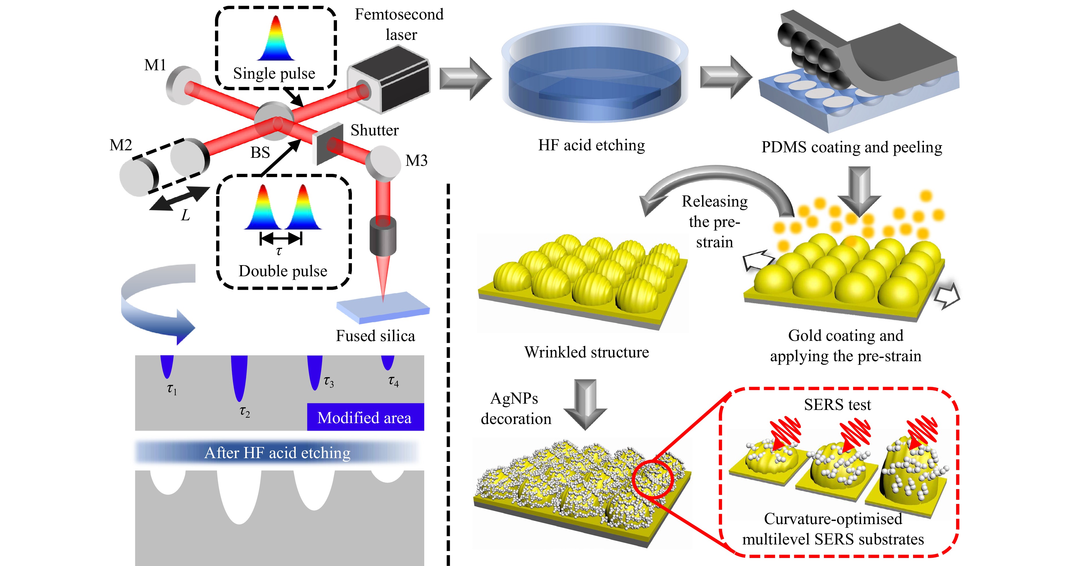
Fig. 1 Schematic of the curvature-optimised multilevel SERS substrate fabrication.
Material modification refers to a phenomenon in which the chemical composition changes after laser irradiation (usually near the material threshold). Essentially, this results from the absorption of photon energy by valence electrons which subsequently transition to the conduction band. Electron transfer leads to chemical bond reorganisation. Silica modification is a process in which large rings within a material undergo cleavage to form three- and four-membered rings35,36. The modification depth under the surface of the fused silica can be precisely controlled by adjusting the pulse delay between the sub-pulses of the double-pulse femtosecond laser, as shown in Fig. 2a. Material modification occurs when the free-electron density reaches a critical threshold. Each sub-pulse irradiates the surface of the material, exciting a certain number of surface free electrons. The depth of the excited free electrons depends on the interaction between two sub-pulses on an ultrafast timescale. Because material modification is a phenomenon that occurs near the energy threshold, the energy of a single sub-pulse is insufficient to cause material modification. Material modification occurs only in the overlapping region.
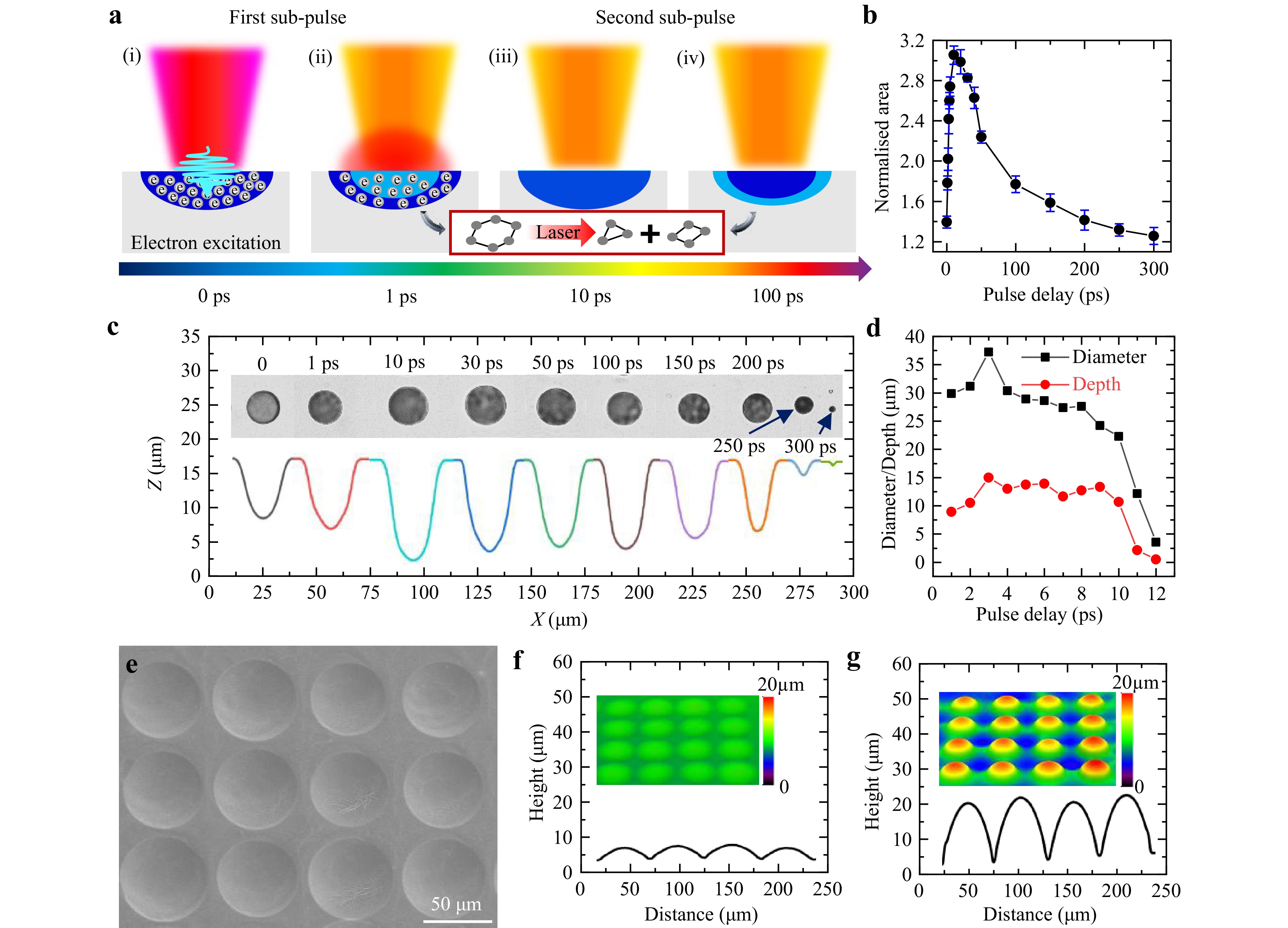
Fig. 2 Fabrication of microlens with different curvatures. a Schematic of microlens fabricated by femtosecond shaping laser. b Normalised area by laser under different pulse delay. c-d Diameter and height of microlens change under different pulse delay. e SEM image of low-curvature microlens array template. f-g Confocal representation of low/high-curvature microlens array and cross-section profile.
The free-electron regions excited by the preceding and succeeding sub-pulses are shown in dark blue and light blue, respectively. As shown in Fig. 2a(i), when the preceding sub-pulse irradiates the material surface, the free-electron density increases. However, this is insufficient for inducing material modification. When the succeeding sub-pulse irradiates the material surface with a pulse delay of 1 ps, as shown in Fig. 2a(ii), a relatively high density of free electrons remains in the region. The accumulation of electrons increased the reflectivity of the material surface. The subsequent sub-pulse energy was then reflected and dissipated. Consequently, the depth of the free-electron region excited by the preceding pulse was greater than that excited by the succeeding pulse. When the pulse delay was 10 ps, as shown in Fig. 2a(iii), the free-electron density excited by the preceding sub-pulse decreased. Thus, the surface reflectivity is reduced. At this point, the excitation depth of the preceding sub-pulse is equal to that of the succeeding sub-pulse because of the balance between the plasma shielding effect and free-electron recombination. Similarly, when the pulse delay reached 100 ps, as shown in Fig. 2a(iv), the region excited by the preceding sub-pulse was significantly diminished. The excitation depth of free electrons by the succeeding pulse was greater than that of the preceding pulse. As the pulse delay increased, the modification depth of the material initially increased and then decreased, reaching a peak at approximately 10 ps.
The variation in modification depth reflects the change in the degree of modification, both of which are related to the amount of photon energy absorbed by the material. The Raman characteristic peaks corresponding to the three-membered and four-membered ring structures are D1 = 495 cm−1 and D2 = 606 cm−1, respectively. The Raman spectra of the modified region is shown in Figure S1. Here, we used the area under the D2 peak to represent the four-membered ring content within the material and compared the degree of modification induced by double-pulse Gaussian beam irradiation with different pulse delays. Baseline correction was performed using the asymmetric least-squares (AsLS) method37. Fig. 2b shows the size of the modified region induced by the double-pulse Gaussian beam within a time-delay range of 0–300 ps. With an increase in the time delay, the concentration of the four-membered ring within the material first increases and then decreases, reaching a peak between 10-20 ps, which indicates that the modification degree is the greatest between 10-20 ps. This result is consistent with our previous findings. Notably, this phenomenon is the most pronounced when the total energy of the dual-pulse is close to the modification threshold of the material. Therefore, we chose the energy of 1 μJ under the focusing conditions of a 20× objective lens for the fabrication.
Subsequently, we used a double-pulse laser with varying pulse delays (0–300 ps) to modify the fused silica surface. The samples were then immersed in 40% HF solution for 2 h. After drying, the cross-sectional morphology of the fabricated microlens was characterised by optical microscopy and confocal profiling is shown in Fig. 2c. Variations in the diameter and depth of the microlens with respect to the pulse delay are illustrated in Fig. 2d. Adjusting the pulse delay enables continuous variations in the diameter of the microlens from 3.5 μm to 37.2 μm, while the depth can be varied from 0.5 μm to 15.0 μm. Simultaneously, the structural dimensions of the microlens can be precisely controlled by adjusting the etching time. Owing to the larger radial contact area of HF, the lateral etching rate exceeds that in the depth direction. Consequently, the microlenses etched for different durations exhibited varying curvatures, as shown in Fig. S2.
We used double-pulse Gaussian laser with pulse delays of 10 ps and 300 ps to modify large-areas of fused silica, followed by etching them into microlens arrays with a diameter of 60 μm for SERS detection. Owing to the varying degrees of modification, different etching durations were required to achieve the same diameter with different pulse delays (Supplement Fig. S3). A 10 ps pulse delay produced a diameter of 60 μm after 4 h of etching, whereas for a 300 ps delay, the same size was achieved in 10 h. Electron microscopy images of the low-/high-curvature microlens arrays after etching are shown in Fig. 2e and S4. The confocal characterisation images of the low- and high-curvature microlens arrays after moulding are shown in Fig. 2f, g, respectively. These images indicate that the curvatures of the microlenses are 0.003 (D = 60 μm, H = 8 μm) and 0.081 (D = 60 μm, H = 23 μm).
Based on the pre-strain deformation mechanism, wrinkles were fabricated on the surfaces of the microlens arrays as shown in Fig. 3a, d. SEM images revealed that the low-curvature substrates formed uniform periodic wrinkles, whereas the high-curvature substrates failed. This phenomenon can be attributed to the geometric characteristics of the high-curvature microlens, which cause strain gradient decay along the axial direction. Despite the significant elastic modulus mismatch between the gold film and the PDMS substrate (EAu = 79-100 GPa, EPDMS = 75 kPa-1.2 MPa), the effective strain did not reach the critical buckling threshold. Consequently, low-curvature microlenses are favourable for the construction of hierarchical micro/nanostructures.
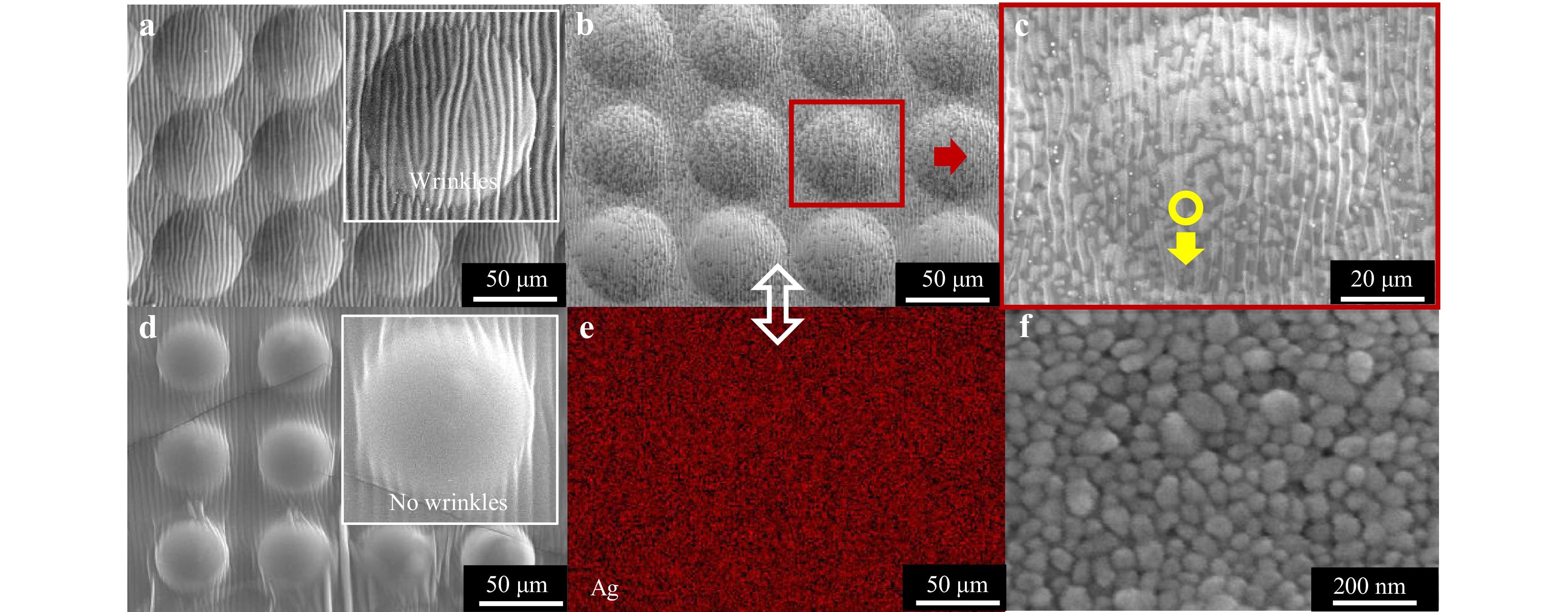
Fig. 3 SEM images of different structures: a Low-curvature microlens with wrinkles b Microlens/wrinkles/AgNPs arrays on the PDMS film. c Singular microlens of Fig. 3b. d High-curvature microlens with wrinkles. e EDS image of Fig. 3b. f Attached AgNPs of Fig. 3c.
Subsequently, the AgNPs were deposited onto the prepared low-curvature microlens/wrinkles arrays. The scanning electron microscopy (SEM) image in Fig. 3b indicates that the synthesised nanoparticles are distributed uniformly, with a small portion appearing as scattered clusters. Fig. 3e shows the corresponding energy-dispersive spectroscopy (EDS) mapping of Ag in Fig. 3b. The Ag nanoparticles are densely and uniformly distributed across the microlens and wrinkle arrays. Fig. 3c shows an enlarged view of the red-boxed region in Fig. 3b. Ordered arrangement of wrinkles and AgNPs is visible on each microlens, and this arrangement is beneficial for the overall uniformity and consistency of the SERS substrate. Fig. 3f shows that the AgNPs are closely connected and densely packed. The nanogaps between the AgNPs significantly increase the number of hot spots per unit area. The size distribution statistics of the AgNPs are shown in Fig. S5.
-
To elucidate the synergistic enhancement mechanism of curvature modulation and multilevel micro-nanostructures in the SERS performance, we establish 3D electromagnetic models using the finite-difference time-domain (FDTD) method, as shown in Fig. 4a. The simulation parameters are set with incident wavelength of 785 nm, power density of 1 mW/cm2, and incident angle of α = 90°. To make the simulation more consistent with the actual conditions and ensure the accuracy of the results, perfectly matched layer boundary conditions were applied. The mesh resolution was set to 0.02 μm. The materials for the gold film and AgNPs were selected from the software material library as Au (gold)-CRC and Ag (silver)-CRC, respectively.
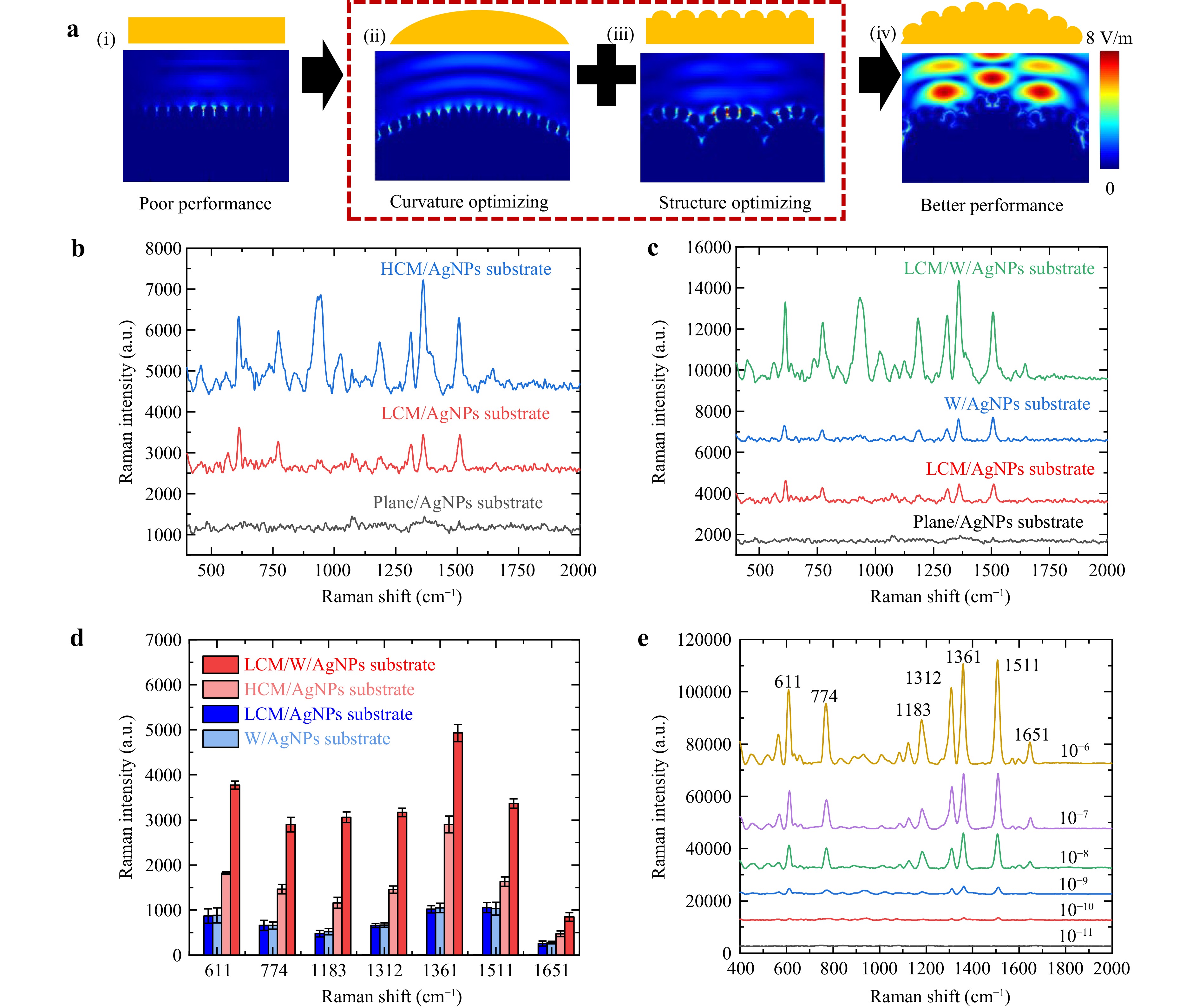
Fig. 4 Curvature optimisation and structural optimisation of SERS substrates. a FDTD simulation for SERS substrate with different structures: (i)-(ii) flat/curved surface, (iii)-(iv) flat/curved surface with wrinkles. b Spectra of SERS substrates with different curvatures. c Spectra of SERS substrates with different structures. d Intensity at each characteristic Peaks in Fig. 4b, c. e SERS spectra of different concentrations of R6G.
In Fig. 4a(i), AgNPs are distributed on flat surface with electric field intensity decaying sharply from the excitation source. AgNPs on curved surface broaden hot spots’ spatial range, creating stronger local electric field [Fig. 4a(ii)]. With wrinkles, localised hot spots between AgNPs are intensified [Fig. 4a(iii)], though overall electric field intensity above remains similar. The 3D hierarchical structure generates widely enhanced electric field above surface, showing sevenfold increase compared to Fig. 4a(i). The statistical data of electric field intensity is presented in Figure S6(e). This enhancement stems from coupling wide-field electric field induced by microlens with plasmonic hot spots on AgNPs and wrinkles. FDTD simulations on structures without AgNPs in Figure S6 show curvature optimisation enhances wide electric field, but the enhancement remains limited. The significant enhancement in Fig. 4a(iv) results from coupling between these effects. Simultaneously micro/nanostructures increase surface “hot spots” density which yields stronger signal intensity. Ultimately, curvature optimisation enhances surface charge accumulation, while structure optimisation increases the density and intensity of the hot spots, both improving the Raman detection performance of the SERS substrate.
To quantitatively assess the effect of curvature and structure optimisation on the SERS performance, we systematically evaluated the system using Rhodamine 6G (R6G, 10−8 M) as a standard probe molecule.
Fig. 4b compares the SERS performances of the substrates with varying curvatures, such as Plane/AgNPs substrates, LCM/AgNPs substrates (Low-curvature microlens/AgNPs substrates), and HCM/AgNPs substrates (High-curvature microlens/AgNPs substrates). As the substrate curvature increased, the corresponding Raman intensity across multiple shifts increased simultaneously. Fig. 4c shows the impact of structural complexity, which increased from bottom to top: Plane/AgNPs substrates, LCM/AgNPs substrates, W/AgNPs substrates (Wrinkles/AgNPs substrates), and LCM/W/AgNPs substrates. The Raman intensity increased with increasing structural complexity. The corresponding intensity of each characteristic peak is shown in Fig. 4d. The enhancement of the microlens or wrinkles was similar, both stronger than that of the planar substrate, but much weaker than their combined effect.
Fig. 4e shows the response of the fabricated SERS substrate to R6G solutions of various concentrations, increasing from the bottom to the top. Even at 10−11 M, distinct characteristic peaks remain visible in the Raman spectra, as shown in Fig. S7(a). The enhancement factor was calculated as EF = (ISERS / NSERS) / (IRS / NRS). At the concentration of 10−6 M, the intensity at 1511 cm−1 reaches 12,385.9, while at 10−11 M, the corresponding intensity is 101.3, giving ISERS / IRS = 122 and NSERS / NRS = 105. Accordingly, the calculated EF is 1.22 × 10⁷. The different intensities of the characteristic peaks are fitted Log-linearly in Fig. S7(b). In addition, we compare the results obtained in this study with those of previous studies38–44 (mainly focusing on micro-nano composite structures with AgNPs), as shown in Fig. S8. Table S1 presents a comparative analysis of the different substrates, focusing on the analytes, detection limits, and enhancement factors. Our approach achieves a lower detection limit owing to curvature and structural optimisation.
-
Uniformity and temporal stability are crucial indicators for evaluating SERS substrates. To test the uniformity of the SERS substrate, we measured the SERS signals at multiple points on a single microlens and at the same positions on different microlenses. Fig. 5a shows the Raman scattering spectra collected from various positions on a single microlens, including 20 spectra from the centre and five from the edge. Fig. 5b presents the corresponding intensities at the 611 cm−1 characteristic peak in each curve. The intralens signal was uniform with a relative standard deviation (RSD) of 6.9%. Fig. 5c shows the intensities of the same peaks from the centres of different microlenses on the same substrate, with an interlens RSD of 3.9%.
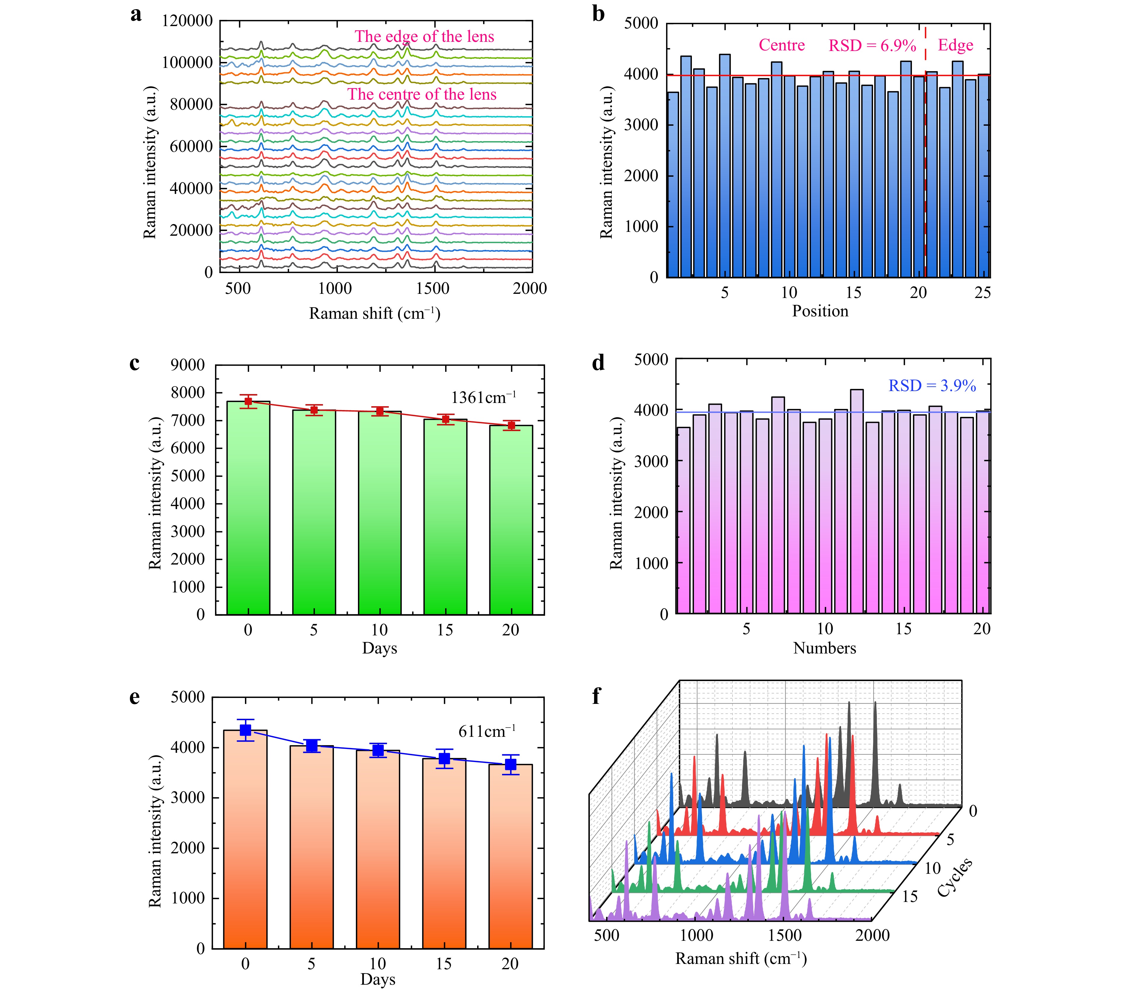
Fig. 5 Uniformity and temporal stability of the SERS substrate. a SERS spectra at 20 different spots (5 spots in the edge and 15 spots in the centre). b Intensity at 611 cm−1 characteristic peaks, and the horizontal line reveals the average value. c Intensity at 611 cm−1 characteristic peaks with different microlens. d-e Changes in the spectral intensity of two characteristic peaks for 20 days. f SERS spectra collected each time after the model has been used.
Fig. 5d, e display the SERS intensity at the characteristic peaks of 611 and 1361 cm−1, measured every 5 days after substrate preparation. As shown in the figures, the Raman intensity of both the characteristic peaks decreases with time. Specifically, the Raman intensity at 611 cm−1 decreases by approximately 14.87%, while that at 1361 cm−1 decreases by ~9.83%. This reduction may be attributed to the oxidation of the AgNPs on the substrate surface when exposed to oxygen in air.
Because the fabricated templates can be replicated and reused multiple times, we also tested the change in the Raman scattering performance after several replication cycles, as shown in Fig. 5f. No significant performance degradation was observed after 0–20 template transfer cycles. The reusability of the template enhanced the fabrication efficiency of SERS substrates. We also evaluated the performance of the flexible substrates under mechanical deformations, including stretching, bending, and twisting, and found that they maintained excellent detection capabilities under all conditions (Supplement Fig. S9).
-
To evaluate the detection performance of the SERS substrate for pesticide residues on the surface of fruits and vegetables, we selected tomatoes and grapes for the detection of thiram, a common fungicide. Thiram is highly effective and has low toxicity in fruits and vegetables. SERS methods include in situ and solution-assisted detection. Fig. 6 details the procedure and results. In situ detection is shown by the blue arrow in Fig. 6a. First, fruit skin was peeled and flattened on a glass slide. The SERS substrate was placed on the fruit skin, with the structured side in direct contact with it. Finally, the slide was placed under the Raman spectrometer to collect Raman scattering light. Since the cured PDMS and the 10 nm gold film are transparent, the Raman scattered light generated by the target molecules under optical irradiation could pass through the substrate and be captured by the objective lens. With a handheld Raman spectrometer, the substrate could attach directly to the fruit surface without the need for peeling.
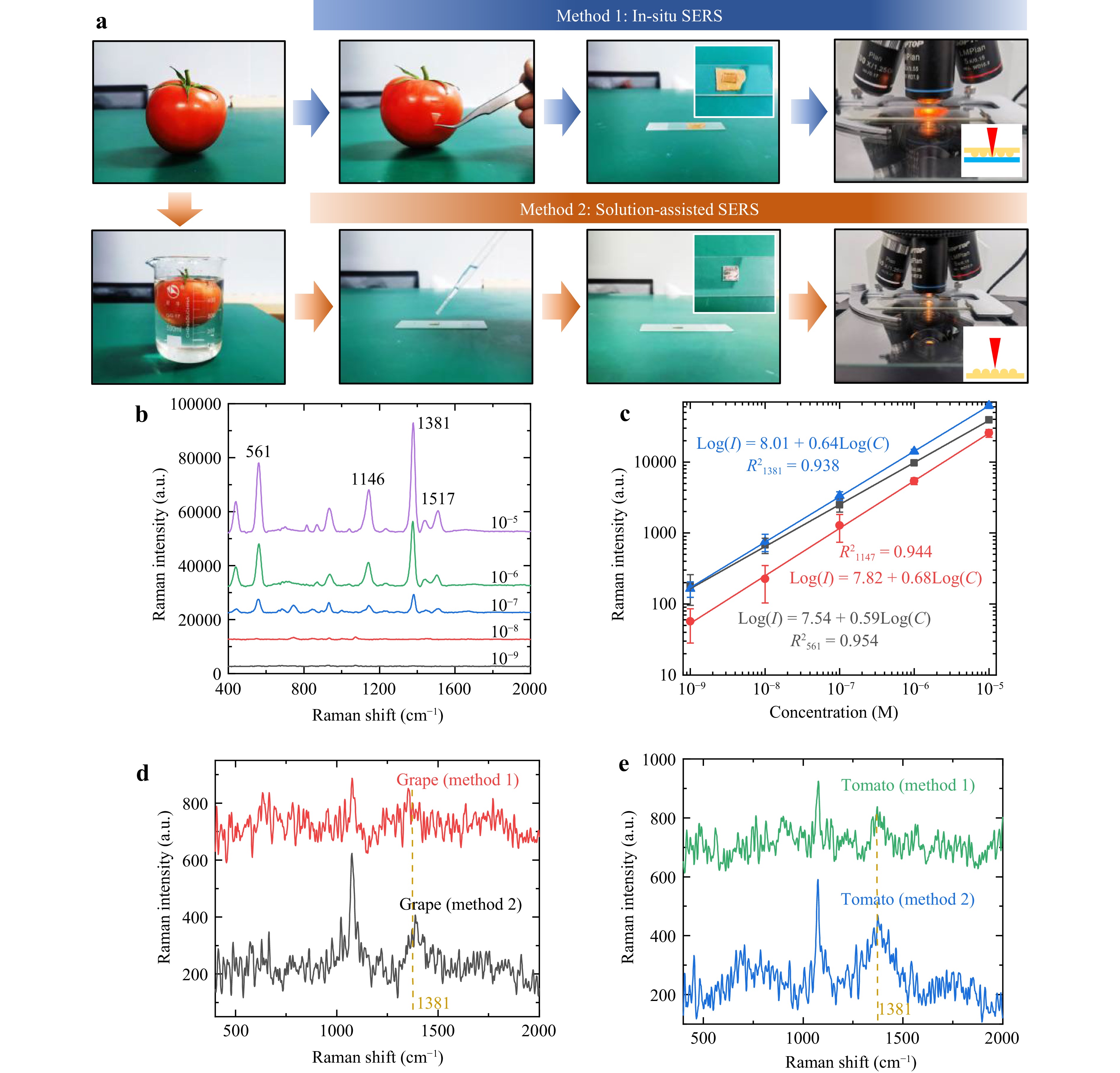
Fig. 6 Detection of thiram pesticide residues. a Two different methods of SERS test: In situ SERS test and solution-assisted SERS test. b SERS spectra of different concentrations of Thiram. c Linear fitting between concentration and SERS intensity, in log scale. d-e SERS test for thiram remain on grapes and tomatoes by Method 1 and Method 2.
Solution-assisted detection is common, shown by the orange arrow in Fig. 6a. First, the fruit was soaked in distilled water for 4 h and then removed. Then, the solution was dropped onto the SERS substrate, allowed to evaporate naturally, and finally placed under a microscope for detection. This solution-assisted detection mechanism suits applications requiring high precision. Fig. 6b shows detection performance at different thiram concentrations, with the fitted line in Fig. 6c. The SERS substrate performs excellently with a minimum detection limit of 10−9 M. Fig. 6d, e presents Raman spectroscopy results for grapes and tomatoes using two methods. For both crops, the substrate shows strong detection at the thiram peak at 1381 cm−1. Compared to Method 2 (solution-assisted detection), Method 1 (in situ detection) shows lower enhancement owing to the reflection of Raman scattered light at the interface.
-
This paper presents a method for fabricating a curvature-optimised multilevel SERS substrate using curvature and structural optimisation strategies. The modification depth of fused silica was controlled by adjusting the delay of the femtosecond laser double pulses. Thus, the curvature of the microlens template changed after etching. Additionally, multilevel micro-nanostructures were created by pre-strain assistance and chemical deposition. The simulation results showed that optimising both the curvature and structure significantly enhanced the localised electric field intensity of the AgNPs on the substrate surface. The fabricated SERS substrate achieved a detection limit as low as 10−11 M, with an EF of AgNPs reaching 1.22 × 10⁷. For the commonly used pesticide thiram, both in situ and solution-assisted detection methods performed well for trace concentration measurements. This approach exhibits the flexibility of femtosecond lasers in processing brittle hard-material templates and offers a promising solution for preparing SERS substrate templates.
-
Fig. 1 illustrates the fabrication process for the microlens arrays. Initially, a femtosecond laser was employed to generate modified regions on a fused silica surface via time-of-flight scanning. The experiment used a regenerative amplified Ti:Sapphire femtosecond laser with 35 fs, 800 nm pulses. The diameter of the laser spot before focusing was 6 mm, with a repetition frequency of 1 kHz and scanning speed of 60 mm/s. The laser power was controlled between the ablation and modification thresholds. Before modification, the fused silica was dominated by a hexacyclic structure formed by silica-oxygen bonding, whereas after modification, the hexacyclic structure was broken into tricyclic and tetracyclic structures. The bond angles of the bridging Si-O-Si bonds in the tricyclic and tetracyclic structures were smaller than those in the hexacyclic structure, resulting in the formation of compact and unstable structures in the focusing region. Changes in the physical structure caused variations in the chemical properties. A decrease in the bond angle increased the activity of the O atom. The prepared fused silica was then immersed in a 40% HF solution, and the following reactions occurred:
$$ \rm \equiv Si-O-Si\equiv + H + F-\to Si-OH + SiF $$ Owing to the high activity of the O atoms in the modified region, the modified region was preferentially etched away during the HF etching. Subsequently, microlenses with smooth bottoms were observed. The depth and width of the microlenses gradually increased with the etching time. After etching, the samples were ultrasonically cleaned with Ca(OH)2 solution and alcohol to obtain clean surfaces. Subsequently, liquid PDMS (Sylgard 184 silicone elastomer; Dow Corning, USA) was mixed with the curing agent on the surface of the SiO2 and placed in a vacuum environment for 30 min to remove bubbles in the PDMS. This step ensured that the PDMS completely infiltrated the microlens on the surface of the mould. Then, the mould covered with PDMS was placed into a vacuum drying chamber at 80 °C for 4 h. The cured PDMS was then demoulded, and a PDMS film with microlens arrays was fabricated.
-
The PDMS film with microlens was stretched by 10% and coated with an Au film (10 nm thick) on the top using magnetron sputtering (80 mA current, 10 s). For controlled stretching, we applied tensile stress using a 1D translation stage (Fig. S10). Upon slow strain release, wrinkles formed on the Au film owing to the different Young’s moduli of Au and PDMS. The wavelength and amplitude of the wrinkles were determined by the following equations45:
$$ {\lambda }_{0}=2\pi h{\left(\frac{{E}_{f}}{3{E}_{s}}\right)}^{\frac{1}{3}} $$ $$ A=h\sqrt{\frac{{\varepsilon }_{pre}}{{\varepsilon }_{c}}-1} $$ $$ {\varepsilon }_{c}=\frac{1}{4}{\left(\frac{3{E}_{s}}{{E}_{f}}\right)}^{\frac{2}{3}} $$ Here, h, Es, and Ef are the film thickness, Young’s modulus of the soft substrate, and Young’s modulus of the hard film, respectively. These equations show that the applied strain and film thickness influence the wrinkle wavelength and amplitude. In the microlens, the tensile strain experienced by the substrate differed from that at the top surface. The magnitude was determined using the strain-transfer function of the structure. The wrinkled cross-sectional profiles were characterised by atomic force microscopy (AFM). The wavelengths of the on-microlens and off-microlens wrinkles were 4.4 and 4.8 μm, and their heights were 1.25 and 1.33 μm, respectively (Fig. S11).
-
Polyvinylpyrrolidone (0.25 g) was added to 30 mL of AgNO3 (0.1 mol/L) solution and dispersed uniformly by ultrasonic vibrations. Next, 1% sodium citrate solution was prepared, and the PDMS film with wrinkles and a microlens was supended in the solution. The solution was heated using a magnetic stirrer, and the stirring switch was turned on when the solution boiled. Simultaneously, 5 mL sodium citrate solution was added to grow the AgNPs and stirred for at least 20 min. Finally, the SERS substrates were cleaned with alcohol and dried in a heating chamber.
-
Different solutions were prepared for testing (different concentrations of R6G, thiram solutions, and epidermal extracts from different fruits). The prepared SERS substrates were immersed in the different solutions for at least 2 h. Then, the RMS1000+ Raman spectrometer was used to acquire their SERS spectra under the following conditions: an excitation wavelength of 785 nm, an integration time of 10 s, and a laser power of 0.1 mW. The laser spot diameter, focused on the sample surface using 50× objective lens (Olympus Inc.; NA = 0.8), was 0.68 µm.
-
The SEM images were captured using a cold-field emission scanning electron microscope (Regulus 8230).
-
This work was supported by the National Key Research and Development Program of China (No. 2022YFB4601300), the National Science Fund for Distinguished Young Scholars (No. 52325505), the National Natural Science Foundation of China (No. 52488301), the National Nature Science Foundation of China (No. 52305444), the National Nature Science Foundation of China (No. 52475321).
Curvature-optimised multilevel SERS substrates formed by femtosecond laser shaping based on electrons dynamics control
- Light: Advanced Manufacturing , Article number: 27 (2026)
- Received: 22 August 2025
- Revised: 19 January 2026
- Accepted: 19 January 2026 Published online: 23 April 2026
doi: https://doi.org/10.37188/lam.2026.027
Abstract: Surface-enhanced Raman scattering (SERS) is widely used for trace detection and compositional analysis of biochemical samples. Constructing multidimensionally ordered hotspots with high densities and intensities is crucial for achieving superior SERS substrate performance. Here, we propose a multilevel SERS substrate based on curvature and structural optimisation strategies. We fabricated microlenses with various curvatures via modification and etching using a temporally-shaped femtosecond laser. These lenses were decorated with wrinkles and Ag nanoparticles (AgNPs) via sequential pre-strain application and chemical deposition. Experimental and simulation results demonstrated that the coupling of the wide-field electric field induced by the microlens with the localised plasmonic hot spots on the AgNPs and wrinkles enhanced the localised surface electric field. Curvature-optimised microlenses can increase the wide-field electric fields. The fabricated SERS substrates achieved a low minimum detection limit of 10−11 M and an enhancement factor of approximately 1.22 × 10⁷. These substrates can be employed to detect thiram fungicide on crops using two different methods (in situ detection and solution-assisted detection), demonstrating potential for operating efficiently under different usage conditions.
Rights and permissions
Open Access This article is licensed under a Creative Commons Attribution 4.0 International License, which permits use, sharing, adaptation, distribution and reproduction in any medium or format, as long as you give appropriate credit to the original author(s) and the source, provide a link to the Creative Commons license, and indicate if changes were made. The images or other third party material in this article are included in the article′s Creative Commons license, unless indicated otherwise in a credit line to the material. If material is not included in the article′s Creative Commons license and your intended use is not permitted by statutory regulation or exceeds the permitted use, you will need to obtain permission directly from the copyright holder. To view a copy of this license, visit http://creativecommons.org/licenses/by/4.0/.

 DownLoad: