


-
In the past decade, optical information processing has garnered significant interest owing to its superior speed and energy efficiency compared to conventional electronic systems1–3. Diffractive optics play a central role in this field, enabling applications such as optical neural networks (ONNs)4–6, holography7,8, information encryption9,10, and optical communications11,12. To facilitate practical deployment and chip-level integration, the development of planar diffractive optical elements (DOEs) with nanoscale resolution has become a key research priority. In the visible spectrum, planar DOEs are typically implemented as diffractive surfaces or metasurfaces13. Diffractive surfaces modulate the optical phase through variations in pixel height or refractive index14,15. Compared to metasurfaces, which rely on geometric or resonance-based phase control16, diffractive surfaces exhibit advantages13 such as reduced transmission loss, lower fabrication cost, simplified fabrication process, and broader spectral compatibility.
Among the various approaches for realising diffractive surfaces, pixel-height modulation via grayscale lithography is particularly attractive owing to its simplicity and compatibility. This enables the construction of multilevel structures by modulating the exposure dose17–19, employing multiple exposures20, or adopting three-dimensional (3D) printing techniques14,21. In particular, laser-based 3D printing directly produces grayscale patterns through multiphoton polymerisation of photoresists22,23. Further integration with galvanometer scanning or projection systems significantly increases the fabrication speed21,24, positioning this method as a mainstream solution for visible-range diffractive optics.
However, existing grayscale lithography techniques face persistent challenges related to resolution and structural reliability. Photoresist-based structures are inherently unstable and susceptible to degradation, which hinders their long-term use in optical systems. To address this, photoresists are often employed as grayscale masks to transfer patterns onto more robust materials, such as SiO2, silicon, or sapphire, via plasma dry etching18,25–28. Nonetheless, previous attempts with laser-printed photoresist masks primarily yielded simple structures such as lenses25 and gratings29. Consequently, current grayscale lithography techniques for robust materials fail to meet the increasing demands of complex, high-resolution diffractive surfaces required for advanced applications such as ONNs and holography. A key limitation is the insufficient lateral resolution of the photoresist masks, typically of the order of several tens of microns25–28, which makes it difficult to realise diffractive features with pixel sizes approaching the visible working wavelengths. In addition, the lack of optimisation of the etching process for anisotropic etching hinders the high-fidelity transfer of grayscale patterns from the photoresist to the substrate. Finally, complex diffractive surfaces require precise phase modulation, which further increases the requirement for etching-rate stability throughout the fabrication process.
To overcome these limitations, we present a high-precision grayscale patterning technique that combines ultrahigh-resolution mask fabrication with a finely tuned dry etching process for a quartz substrate (Fig. 1a-c). High-resolution grayscale photoresist masks are fabricated using femtosecond laser-nanoprinting. Fine pattern transfer onto the substrates is achieved through combined multiparameter optimisation of the dry etching process, with key parameters, including gas composition, power, and pressure, which must be carefully tuned. This approach achieves pattern transfer at a resolution of approximately 81 nm and supports eight discrete phase levels with 1 μm2 pixel sizes. Representative grayscale patterns such as a “Chinese dragon” and a “flower” were successfully fabricated with nanoscale fidelity (Fig. 1d, e). The number of phase modulation levels plays a critical role in diffractive performance. Notably, increasing the number of grayscale levels significantly enhances the diffraction efficiency, as demonstrated using blazed gratings (Fig. 1f). Moreover, the use of quartz substrates ensures exceptional thermal and mechanical stability, making the structures suitable for practical integration. Importantly, this technique is not limited to quartz and is compatible with silicon wafers, thereby extending its applicability to both optical and electronic devices. Based on this method, we further demonstrate diffractive surfaces with complex phase distributions, such as multilevel holograms, lenses, and DNNs (Fig. 1g). Notably, the fabricated DNN achieves a classification accuracy of 91.75% on a four-class MNIST dataset. These results represent a substantial advancement toward scalable, high-fidelity, and durable fabrication of multifunctional diffractive optical devices.
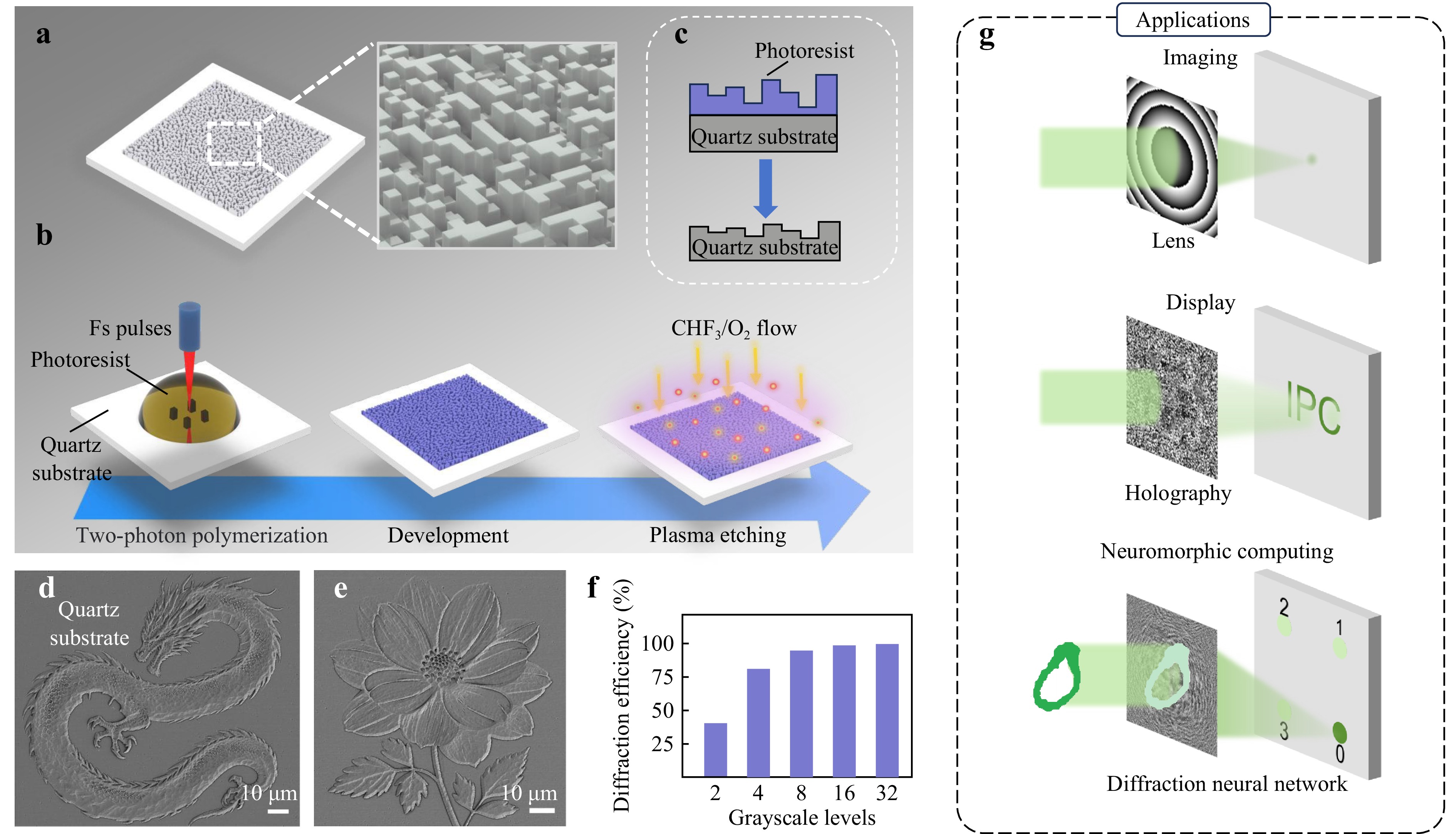
Fig. 1 Principle of the grayscale patterning technique on quartz substrate. a Schematic illustration of the morphology of diffractive surfaces fabricated using the proposed technique. b High-precision grayscale lithography achieved via a single-step lithography and dry etching process. c Schematic of grayscale pattern transfer from the photoresist mask to the substrate through optimized etching. d, e High-resolution grayscale patterns—a “Chinese dragon” and a “flower”—fabricated on quartz substrates. f Calculated 1st-order diffraction efficiency of blazed gratings as a function of phase modulation levels, highlighting the advantage of multi-level phase modulation. g Demonstrated applications of the technique, including lenses, holograms, and DNN.
-
Grayscale etching on quartz substrates differs fundamentally from conventional etching methods. In this process, the photoresist mask must be completely removed to ensure a successful grayscale pattern transfer to the substrate. The diffractive surface achieves transmission-type phase modulation by controlling the pixel height5. At different operating wavelengths, each pixel requires a specific etching depth to achieve accurate multilevel phase modulation. Therefore, accurate pattern transfer and uniform etching rates for both the photoresist and the substrate must be achieved through the etching process. In the mask-printing stage, a high-resolution photoresist (IP-dip) and a high numerical aperture objective (Plan-Apochromat 63x/1.40 Oil DIC, Zeiss) were employed to obtain nanoscale-resolution masks. Two-photon polymerisation enables mask fabrication with nanoscale resolution beyond the diffraction limit, thereby providing a critical foundation for high-precision etching. Subsequently, the etching parameters were systematically optimised to enable high-precision pattern transfer onto a quartz substrate (Fig. 2).
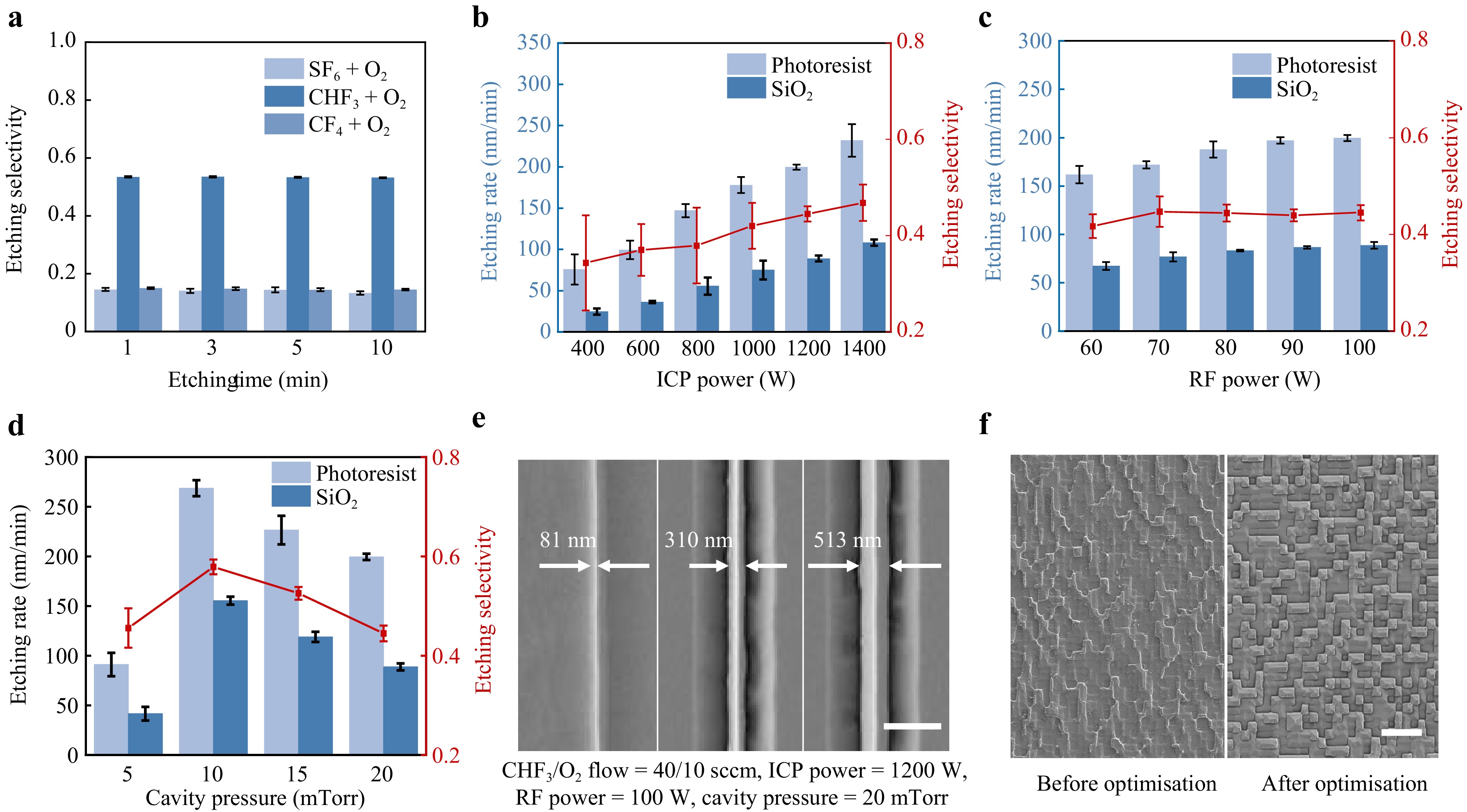
Fig. 2 Multiparameter optimisation of etching conditions for high-precision grayscale pattern transfer on quartz substrate. a Etching selectivity of quartz-to-photoresist as a function of etching time under different gas compositions. The total gas flow rate was maintained at 50 sccm, with SF6, CHF3, and CF4 each at 40 sccm and O2 at 10 sccm. b Etching rate and selectivity as a function of ICP power. c Etching rate and selectivity as a function of RF power. d Etching rate and selectivity as a function of chamber pressure. e SEM images showing different etched lateral line widths achieved using the optimized parameters. Scale bar: 1 μm. f Comparison of SEM images of diffractive surfaces before (using empirical SiO2 etching parameters: SF6/O2 = 40/10 sccm, ICP = 1000 W, RF = 90 W, pressure = 20 mTorr) and after parameter optimisation, demonstrating enhanced etching fidelity. Scale bar: 5 μm.
To achieve high-fidelity pattern transfer, it is critical to suppress lateral etching of the photoresist mask. The dry etching process employs inductively coupled plasma reactive ion etching (ICP-RIE), where chemically reactive species generated by gas ionisation react with the substrate, while ion bombardment induces physical reactions30. Therefore, the etching process involves both physical and chemical mechanisms.
Chemical etching, which is mainly governed by the gas composition, is typically isotropic and is primarily responsible for the lateral etching of the photoresist. Therefore, we investigated the effects of different etching gases—SF6, CHF3, and CF4—on the overall etching performance. Fig. 2a shows the etching selectivity between quartz and photoresist. The etching selectivity, R=Squartz/Sphotoresist, is defined as the ratio of the etching rate of quartz (Squartz) to that of the photoresist mask (Sphotoresist). The etching rates of the quartz and photoresist were obtained by measuring their respective etching depths over a specified period using a step profiler and then dividing by the etching time (Methods). Note that CHF3 exhibits a smaller error bar in the etching selectivity between quartz and photoresist, indicating improved etching rate stability. More importantly, CHF3 yields distinct etching selectivity, primarily because of its reduced photoresist etching rate. The measured photoresist etching rates were approximately 563 nmmin−1 (SF6 + O2), 165 nmmin−1 (CHF3 + O2), and 843 nmmin−1 (CF4 + O2). This lower etching rate is likely attributable to the reduced fluorine content of CHF331. Consequently, achieving the same substrate-etching depth as CHF3 requires a thinner photoresist mask, which helps reduce the lateral etching of the photoresist mask and enables finer pattern transfer. The error bars were determined by measurements taken at multiple positions across a 2.5 cm × 2.5 cm sample. Before each experiment, we performed equipment ambientization to maintain consistency across different runs. The addition of oxygen helps stabilise the photoresist etching process. The oxygen plasma participates in chemical etching, leading to a more uniform removal rate. In contrast, without oxygen, the photoresist is thinned mainly by physical ion bombardment, which can induce surface cross-linking32 and cause variations in the etching rate during processing. As shown in Fig. S1, the introduction of oxygen significantly improves the stability of the photoresist etching rate, resulting in a more consistent etching selectivity between quartz and photoresist.
In addition to gas composition, both the ICP and radio frequency (RF) powers significantly influence the stability and quality of the etching process (Fig. 2b, c). Within an optimal range, increasing both the ICP and RF powers enhances the etching rate and the etching rate stability. A higher etching rate helps shorten the total etching time, thereby minimising substrate heating, which can otherwise degrade speed stability33,34. An ICP power of 1200 W and an RF power of 100 W yielded the best results; beyond this, the performance declined owing to power instability. Moreover, more surface defects were observed at lower RF power (Fig. S2). The chamber pressure is another critical parameter. The patterns transferred after etching under low pressure had lower fidelity (Fig. S3). At a pressure of 20 mTorr, the etching process exhibited an improved etching rate stability (Fig. 2d) and yielded surfaces with minimal defects (Fig. S4). These findings highlight the necessity of coordinated multiparameter optimisation for stable and precise grayscale pattern transfer.
Following this optimisation, stable etching rates were achieved for both quartz substrates and photoresist masks, with a final etching selectivity of R = 0.43. The etching parameters were finally set as follows: SF6/O2 = 40/10 sccm, ICP power = 1200 W, RF power = 100 W, and chamber pressure = 20 mTorr. Using these optimised parameters, we achieved a minimum feature lateral linewidth of 81 nm on the quartz substrate (Fig. 2e), whereas the corresponding photoresist mask exhibited a linewidth of approximately 100 nm. The deviation between the mask and quartz linewidths primarily originates from lateral etching during the dry-etching process. As discussed earlier, the chemical reactions involved in plasma etching are typically isotropic and contribute to etching in all directions. Although this effect was suppressed through multiparameter optimisation, a certain degree of lateral etching remains, resulting in a reduced final linewidth compared to that of the photoresist mask. Because both the photoresist mask fabrication and dry-etching processes are isotropic in the x- and y-directions, the achieved lateral resolution of 81 nm applies equally along both axes. Fig. S5 shows the etching results for different values of lateral linewidth and line spacing.
For comparison, Fig. 2f presents scanning electron microscopy (SEM) images of grayscale patterns etched with a pixel size of 1 μm2 using unoptimised empirical parameters—originally developed for standard SiO2 films in our laboratory—and those obtained under optimised etching conditions. The results highlight a substantial improvement in pattern fidelity. Lateral etching persisted after optimisation, as evidenced by the tilted SEM images (Fig. S6). Nevertheless, by comparing the degree of lateral etching before and after optimisation, it can be seen that lateral etching was greatly reduced (Fig. S7).
Moreover, this technique is compatible with silicon wafers, as shown in Fig. S8. While our main focus is on quartz substrates for diffractive surface fabrication, we further investigated and optimised etching parameters on silicon to extend the scope of this approach. The results demonstrate that beyond diffractive optics, the method can be applied to silicon-based grayscale patterning, highlighting its potential for integrated photonic and electronic devices.
-
High-precision functional diffractive surfaces were fabricated on quartz substrates to demonstrate the versatility of the proposed technique. As a representative sample, an 8-level phase-modulated hologram (100 × 100 pixels with a pixel size of 1 μm2) was designed using the Gerchberg-Saxton algorithm35 to reconstruct the letters “IPC” (Institute of Photonic Chips). We selected 8-level phase modulation for two reasons. First, laser-printed masks employ a piezoelectric displacement stage for grayscale height control. Although the stage provides ±10 nm displacement accuracy—sufficient for higher-order grayscale masks—additional levels would substantially increase fabrication time. Second, as shown in Fig. 1f, 8-level phase modulation already achieves high diffraction efficiency for diffractive elements, meeting the requirements of holographic displays and representing a widely adopted standard in diffractive optics36–38. With this choice, the entire fabrication process, including both laser-nanoprinting and dry etching, was completed in less than 20 min, with the laser printing step requiring only approximately 2 min.
For a working wavelength of 532 nm, the required etching depths for each phase level were calculated using the equation φ(λ) = 2π(n − 1)h/λ5,7, where φ(λ) is the phase shift at wavelength λ, n is the refractive index of quartz (approximately 1.5), and h is the etching depth. These calculations were matched with the experimentally determined etching selectivity (R) to define the corresponding height of the photoresist mask. Fig. 3a illustrates the optical setup used for holographic testing. For comparison, a hologram with the same design was fabricated directly on the photoresist. Owing to the similar refractive indices of IP-Dip and quartz, the atomic force microscopy (AFM) measurements showed that the two structures exhibited comparable feature heights (Fig. S9). It should be noted that, owing to the principle of two-photon polymerization22, the effective exposure volume is confined to the focal region of the objective, producing an ellipsoidal solidified structure with intrinsically rounded edges. The AFM images reveal that the mask pixels possess smooth edge profiles.
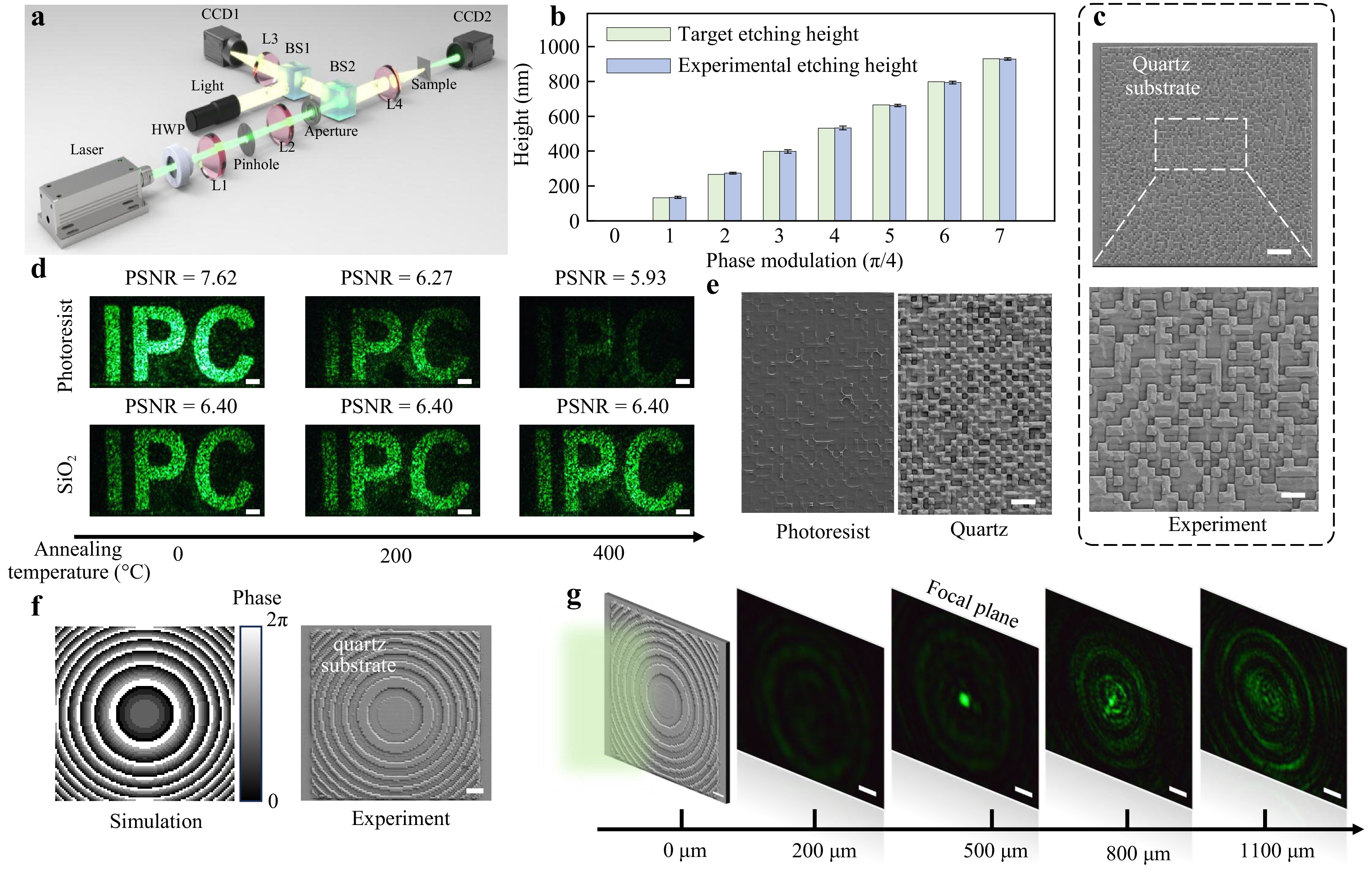
Fig. 3 Quartz-based high-precision diffractive surfaces for holography and lensing. a Optical setup for hologram testing. b Target grayscale etching depths and corresponding experimental results for an 8-level phase modulation diffractive surface working at 532 nm laser. c SEM images of the fabricated hologram at different magnifications. Scale bars: 5 μm (top), 2 μm (bottom). d Holographic images reconstructed from photoresist-based (top) and quartz-based (bottom) holograms after annealing at various temperatures for 30 min. Scale bar: 1 mm. e SEM images of the two holograms after annealing at 400 °C for 30 min. Scale bar: 5 μm. f Calculated phase distribution and corresponding SEM image of the diffractive surface designed for lensing. Scale bar: 10 μm. g Captured intensity profiles of the light field at different propagation distances after transmission through the diffractive lens. Scale bar: 0.1 mm.
Fig. 3b shows that the measured average step height between adjacent phase levels was approximately 132.53 nm, which confirms the agreement between measured and designed etching depths, supporting the accuracy of the fabrication process. Although lateral etching was effectively suppressed, minor surface nonuniformities were still observed; thus, the etching depth data in Fig. 3b were obtained primarily from the central regions of the pixels to ensure measurement consistency. The final morphology of the hologram is shown in Fig. 3c, demonstrating high structural fidelity.
The quartz-based diffractive surface exhibited superior stability under extreme environmental conditions. To assess thermal robustness, both the quartz and photoresist-based holograms were subjected to annealing. As shown in Fig. 3d, the initial display quality and peak signal-to-noise ratio (PSNR) were higher for the photoresist hologram. However, following thermal treatment at 400 °C, the photoresist hologram exhibited significant structural degradation, whereas the quartz-based structure remained intact. This observation was confirmed by the SEM images shown in Fig. 3e. The PSNR values of the holographic images before and after annealing were calculated (Fig. S10). In addition, the chemical resistance was evaluated via acid treatment, and the quartz-based hologram showed no apparent damage (Fig. S11), which further demonstrates its environmental durability.
A diffractive lens with a focal length of 500 μm was also fabricated to validate the general applicability of the technique. As shown in Fig. 3f, the fabricated phase profile closely matched the design target. Optical characterisation showed that the lens successfully focused incident light at the intended distance of approximately 500 μm, consistent with the theoretical predictions of lens performance (Fig. 3g). The diffraction efficiency measured using a beam profiler was approximately 71% (Fig. S12). This is slightly lower than the theoretical value of 86.08%, with the discrepancy primarily attributed to fabrication inaccuracies, namely the resolution limit of the laser-printed mask and lateral etching effects during the grayscale pattern transfer.
-
ONNs, which use light as an information carrier, have attracted significant research interest owing to their ultralow energy consumption and ultrahigh processing speed2,3. Among various ONN architectures, DNNs, a class of free-space ONNs, stand out for their high-throughput computational capabilities4,39,40. As illustrated in Fig. 4a, DNNs modulate light fields through phase-encoded neurons, whereas the weighted multiplication and summation operations between neurons are implemented via optical diffraction and coherent interference. Owing to their inherent 3D architecture, laser-nanoprinting has emerged as a widely used method for DNNs4,14,41. However, existing implementations based on photoresist structures have limitations in terms of their long-term reliability, particularly under thermal or chemical stress.
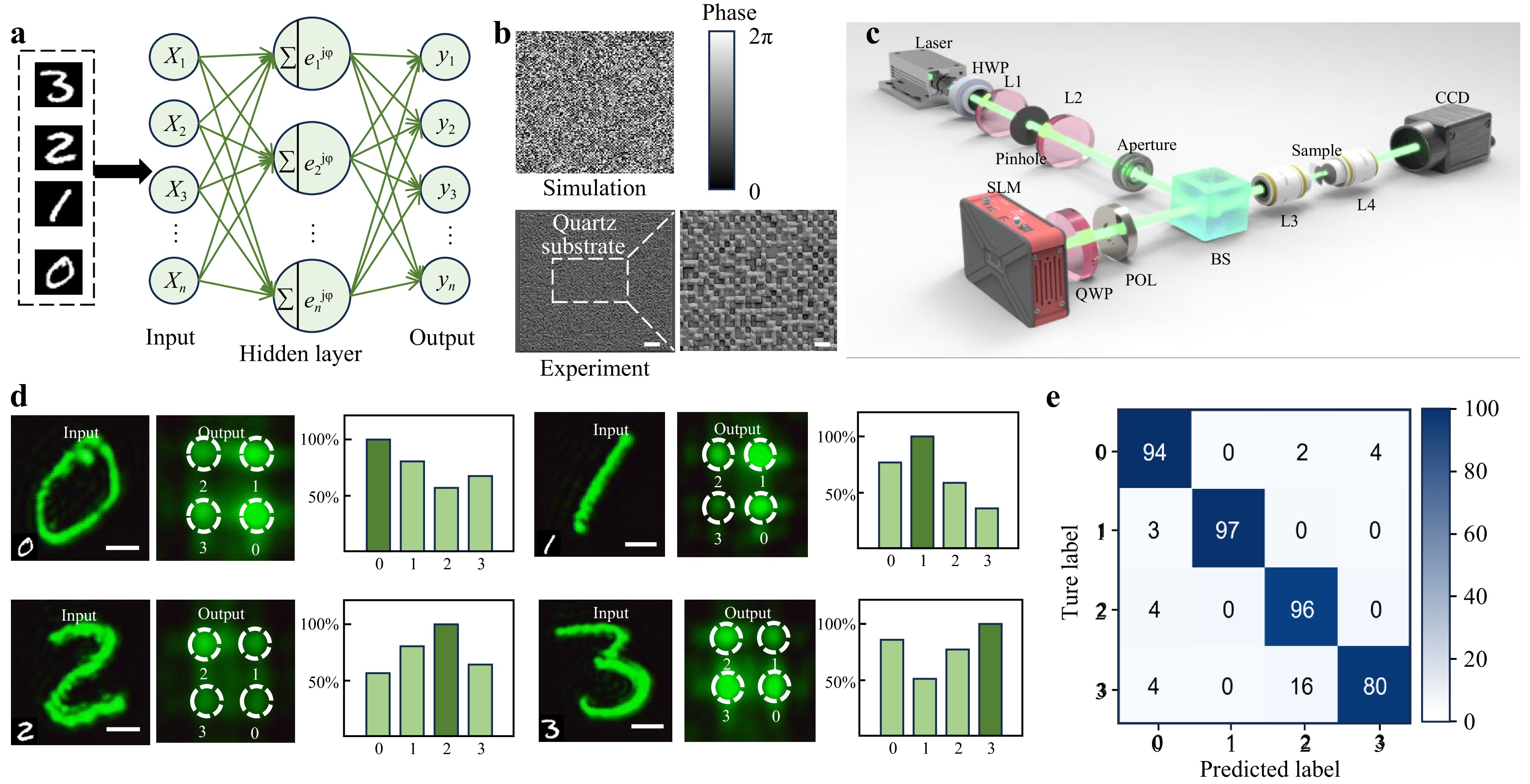
Fig. 4 Quartz-based high-precision diffractive surface for DNN application. a Schematic illustration of the mathematical operation flow of the diffractive neural network (DNN). b Phase distribution obtained after training and corresponding SEM images of the fabricated diffractive surface (scale bars: 10 μm and 3 μm). c Optical setup used for DNN testing. d Example input image, resulting output light field, and normalised output intensities corresponding to each detection region; scale bar: 0.1 mm. e Confusion matrix of the DNN for classification results over 400 test images.
In this study, we demonstrate the fabrication of a single-layer DNN (100 × 100 pixels with a pixel size of 1 μm2) directly on a quartz substrate using this technique. The DNN was trained on the MNIST dataset, which comprises 2,000 images (500 per class), using Google TensorFlow 2.6.0. The phase profile of the diffractive layer was optimised using back-propagation and gradient descent (Fig. S13a). To enhance performance, the propagation distance between the input and output layers was optimised based on the Fresnel number42, achieving a training accuracy of 96.6% (Fig. S13b). Fig. 4b presents the resulting phase distribution and fabricated DNN surface morphology. The optical setup is shown in Fig. 4c. Input patterns43 were encoded using a spatial light modulator (SLM), in combination with a quarter-wave plate (QWP) and a polariser. By appropriately selecting the fast-axis angle of the QWP, orientation of the polariser, and phase setting of the SLM, this configuration enables amplitude-based image encoding without introducing additional phase profiles (Fig. S14 and Note 1). Consequently, the potential phase noise in the input images is reduced, which has been demonstrated to negatively affect the recognition performance of DNNs44. The output patterns were captured using a charge-coupled device (CCD) camera placed downstream of the DNN and aligned in a 4f optical configuration. Representative input images and corresponding output results for handwritten digits are shown in Fig. 4d. For each input digit, the correct detection region among the four white dashed circles exhibited the highest intensity, indicating successful classification by the DNN. The DNN was evaluated using 400 test images (100 images from each category). The confusion matrix shown in Fig. 4e reveals that the DNN achieves a classification accuracy of 91.75%, thus confirming the effectiveness of the diffractive structure. It should be noted that the DNN can, in principle, support more classification categories, but its accuracy decreases significantly (Fig. S15a). Thus, in addition to increasing the number of diffractive layers, the simulations suggest that increasing the pixel count within each layer can provide notable performance gains (Fig. S15b). Increasing the number of pixels requires enlarging the printed etching-mask area. A practical approach is to divide a large etching mask into multiple subregions and print them sequentially.
In summary, we developed a laser-nanoprinting-based grayscale lithography technique combined with multiparameter etching optimisation to achieve high-precision pattern transfer onto a quartz substrate. This approach enabled the fabrication of multilevel diffractive surfaces with nanoscale resolution (~81 nm), supporting eight discrete phase levels within 1 μm2 pixels. Compared to conventional grayscale lithography, the proposed method overcomes critical resolution limitations and improves long-term material stability. Its effectiveness has been validated by the successful realisation of functional diffractive devices, including holograms and diffractive neural networks. The fabricated surfaces exhibit lateral dimensions down to 100 μm, high structural fidelity, and operational durability, thereby addressing key demands in the development of compact, reliable, and highly integrated photonic systems. To further improve the grayscale patterning resolution, future work may involve the adoption of two-beam laser writing techniques22,45,46, which offer enhanced spatial control and mask definition.
Compared with photoresists, quartz and silicon exhibit much higher mechanical strength and chemical stability, ensuring superior durability and reliability. Therefore, diffractive structures fabricated on these substrates can operate stably under diverse conditions, including extreme environments such as strong radiation, high temperatures, and deep-sea and deep-space settings. Consequently, the proposed method offers enhanced flexibility and broader practical potential than photoresist-based approaches.
In terms of specific applications, the demonstrated technique is particularly promising for integrated photonic systems, except for conventional diffractive elements such as holograms and lenses. The use of quartz or Si substrates offers enhanced structural robustness and integration compatibility. This enables monolithic integration of diffractive surfaces with a wide range of nano- and micro-scale optical components. For instance, they can be directly implemented on optical fibre end faces for beam modulation47 and in-fibre imaging6, or integrated with light sources such as vertical-cavity surface-emitting lasers for applications such as vortex beam generation21,48 and holography49. This level of compatibility facilitates the development of compact actively modulated photonic devices. To further broaden their applicability, we investigated and optimised the etching parameters for silicon wafers, thereby extending this technique to a wider set of platforms. Overall, the demonstrated technique provides a versatile platform for the fabrication of high-resolution diffractive structures with potential applications in integrated photonics, optical computing, and optoelectronic systems.
-
The fabrication process for diffractive surfaces on a quartz substrate is illustrated in Fig. 1b. First, the etching masks were printed using a commercial two-photon lithography system (Photonic Professional GT, Nanoscribe GmbH), equipped with a 780 nm, 80 MHz femtosecond laser. This system includes a high-numerical-aperture immersion objective (Plan-Apochromat 63×/1.40 oil phase contrast, Zeiss) in the galvanometer scanning mode. A two-photon photoresist (IP-Dip) was used as the printing material. Commercial 1-inch quartz substrates (thickness: 0.5 mm) were used. The diffractive phase plates were designed with a resolution of 100 × 100 pixels and a pixel area of 1 μm2. Based on the experimentally determined etching selectivity, the hatching distance was set to 0.05 μm, and the height gradient of the photoresist mask was set to 0.306 μm. After etching, this yielded diffractive surfaces with a height gradient of approximately 0.133 μm, corresponding to a phase modulation of ¼π at a working wavelength of 532 nm. The optimised laser power and scanning speed were 18 mW and 10,000 μm·s−1, respectively. After laser printing, the samples were developed in propylene glycol methyl ether acetate for 25 min, rinsed with isopropanol for 5 min, and then dried.
-
Grayscale pattern transfer onto the quartz substrate was achieved by fully etching the photoresist mask using an Oxford etching system (Plasmalab System 100, Oxford Instruments). To ensure process stability, a 6-inch Si wafer was initially placed in the etching chamber and cleaned with oxygen plasma for 30 min. A 15-min ambientization step was then performed to confirm the chamber cleanliness using the same parameters as those employed in the real etching process.
During etching, the quartz substrate was bonded to a Si wafer using thermal grease to prevent excessive heating. The etching parameters were as follows: CHF3 flow rate, 40 sccm; O2 flow rate, 10 sccm; ICP power, 1200 W; RF power, 100 W; and chamber pressure, 20 mTorr. After etching, the samples were ultrasonically cleaned with ethanol for 30 min.
When characterising the etching selectivity shown in Fig. 2, the etching rates of the quartz and photoresist were determined by measuring their etching depths over a specified time period using a step profiler and dividing the measured depth by the etching duration. First, the initial thickness of the photoresist mask (dphotoresist) was measured. After etching for a specified time t while a portion of the photoresist mask remained, the total height of the etched structure (d1) was measured. At this stage, d1 = dphotoresist′ + dquartz, where dphotoresist′ is the remaining photoresist thickness after etching, and dquartz is the etching depth of quartz. The photoresist was then removed and the quartz etching depth dquartz was directly measured using the step profiler. Accordingly, the quartz etching rate is Squartz = dquartz/t, and the photoresist etching rate is Sphotoresist = (dphotoresist − dphotoresist′)/t = (dphotoresist − d1 + dquartz)/t.
-
A 532 nm solid-state laser was used as the light source for all optical characterisations. A 4f optical system was used to control the beam diameter. For hologram testing, the laser beam was directed onto the hologram using an additional lens (L4 in Fig. 3a), which focused the beam and performed the Fourier transform. An auxiliary imaging path composed of an illumination source and lenses was incorporated to ensure precise spatial alignment between the incident beam and the hologram.
For DNN testing, an SLM (EXULUS-HD2, Thorlabs) was introduced into the optical path. This configuration enabled the generation of amplitude-modulated input signals in conjunction with a quarter-wave plate and polariser (Supplementary Note 1). The DNN sample was positioned between the two objective lenses (L3 and L4 in Fig. 4c), forming a 4f system for testing. All output signals were captured using a CCD camera.
For structural characterisation, SEM images were acquired using a ZEISS Sigma 300 microscope, and AFM measurements were performed using a Bruker Dimension Icon system.
-
DNN training was performed using TensorFlow 2.6.0. The input images from the MNIST dataset were resized to 100 × 100 pixels to match the network dimensions. The forward propagation of the optical field was simulated using the angular spectrum method to account for light diffraction50. A cross-entropy loss function was defined based on the predicted outputs and true labels. The phase distribution of the diffractive layer was iteratively optimised using backpropagation and gradient descent. To enhance performance, the distances from the input and output layers to the diffractive layer were optimised based on the Fresnel number, and set to 1900 μm and 6600 μm, respectively. The training was conducted during 300 epochs with a learning rate of 0.03.
-
The diffraction efficiency shown in Fig. 1f was calculated based on the Fourier theory (scalar diffraction theory)51, the core of which is to expand the transmission function of the periodic step structure of the element into a Fourier series and obtain the sub-efficiency of each diffraction level by squaring the coefficients. For blazed gratings, the n-order diffraction efficiency is given by
$$ {\eta }_{n}={\left[\frac{\sin \left({\text{π}} n/ N\right)}{{\text{π}} n/ N}\right]}^{2} $$ where N is the number of steps.
-
We acknowledge the support from the National Key Research and Development Program of China (2022YFB2804301), the Science and Technology Commission of Shanghai Municipality (Grant No. 21DZ1100500), the Shanghai Municipal Science and Technology Major Project, the Shanghai Frontiers Science Center Program (2021–2025 No. 20), and the Shanghai Sailing Program (23YF1429500).
Laser-nanoprinting-enabled multilevel nanoscale phase encoding on quartz for integrated optical diffractive devices
- Light: Advanced Manufacturing , Article number: 31 (2026)
- Received: 26 June 2025
- Revised: 22 January 2026
- Accepted: 03 February 2026 Published online: 23 March 2026
doi: https://doi.org/10.37188/lam.2026.031
Abstract: To overcome the resolution and stability limitations of conventional grayscale lithography, we present a laser-nanoprinting-assisted technique for multilevel nanoscale phase encoding on a quartz substrate. The proposed approach combines femtosecond laser-based grayscale mask fabrication with multiparameter dry etching optimisation to achieve precise phase modulation with subwavelength resolution approximately 81 nm) and pixel sizes as small as 1 μm2. Up to eight discrete phase levels are supported, enabling efficient diffraction control and device-level functionality. Using this method, various integrated diffractive devices, including lenses, holograms, and diffractive neural networks (DNNs), were realised on quartz substrates. The fabricated structures exhibit high pattern fidelity, mechanical and chemical robustness, and compatibility with standard photonic integration platforms. Notably, a single-layer quartz-based DNN achieved a classification accuracy of 91.75% across four classes of handwritten digits. This nanoprinting-enabled strategy provides a scalable and stable pathway for fabricating compact, multifunctional, and high-resolution diffractive photonic devices.
Research Summary
Grayscale lithography: Nanoscale Phase Encoding Technique
A high-resolution laser-nanoprinting technique combined with optimized dry etching enables the fabrication of durable, multilevel diffractive devices on quartz substrates. Haitao Luan et al. developed a grayscale lithography technique for quartz-based multilevel nanoscale phase encoding. It combines femtosecond laser grayscale masks and optimized dry etching, achieving ~81 nm resolution and 8 phase levels in 1 μm² pixels. The team fabricated robust lenses, holograms, and a diffractive neural network with 91.75% handwritten digit classification accuracy, advancing compact, high-performance photonic integration.
Rights and permissions
Open Access This article is licensed under a Creative Commons Attribution 4.0 International License, which permits use, sharing, adaptation, distribution and reproduction in any medium or format, as long as you give appropriate credit to the original author(s) and the source, provide a link to the Creative Commons license, and indicate if changes were made. The images or other third party material in this article are included in the article′s Creative Commons license, unless indicated otherwise in a credit line to the material. If material is not included in the article′s Creative Commons license and your intended use is not permitted by statutory regulation or exceeds the permitted use, you will need to obtain permission directly from the copyright holder. To view a copy of this license, visit http://creativecommons.org/licenses/by/4.0/.

 DownLoad: