


-
Integrated photonics offers significant opportunities for miniaturisation and scalability in both digital and analogue applications related to information processing and routing. Miniaturised high-speed receivers and transmitters1,2, optoelectronic signal generators with high phase stability3, optical sampling and routing for analogue-to-digital conversion4,5, and fibre-optic environmental sensors6 have emerged as key applications of integrated optical signal processing. Silicon photonics (SiPh) is particularly advantageous for achieving extremely compact designs. The high refractive index contrast of constituent materials, together with advanced CMOS fabrication technologies, enables high-performance components with dense integration7,8. Furthermore, the high thermo-optic coefficient facilitates broadband wavelength tuning and kHz-rate fast scanning functionality9.
Despite these advantages, the realisation of high-speed modulators on silicon platforms remains challenging. The most widely used silicon modulation approach relies on the inherently weak plasma dispersion effect in p–n junction regions10. This typically necessitates millimetre-scale Mach–Zehnder interferometers (MZIs), which convert electro-refraction into intensity modulation. Although resonant modulators can achieve smaller footprints, they require more complex stabilisation due to strong dispersion under resonant conditions11. In modern high-resolution signal processing systems, balanced detection—often essential—requires modulators capable of producing dual outputs with a π phase shift5,12,13. In conventional MZI-based systems, this phase difference between the dual-output signals is governed by the coupler design. However, such functionality is rarely realised in compact devices. Therefore, the development of a compact silicon intensity modulator with dual-output capability remains highly desirable.
Ultra-compact integrated electro-optical modulators based on transparent conductive oxides (TCOs), such as indium tin oxide (ITO)14,15, indium oxide16, aluminium zinc oxide17, and cadmium oxide18, have attracted considerable attention. These materials exhibit significant changes in refractive index when an applied electric field alters the electron distribution. Variations in both the real and imaginary components of the refractive index enable simultaneous refractive and absorptive modulation mechanisms.
Typically, modulation is achieved using a capacitor structure integrated directly onto a silicon waveguide, with the TCO layer serving as one of the capacitor electrodes. Changes in electron concentration are confined to a thin (~2 nm) accumulation layer (ACL)19 at the interface between the TCO and the insulating layer. Such hybrid plasmonic waveguides (HPWGs) enable efficient coupling between the silicon waveguide mode and the electro-optical capacitor20–23. Most reported HPWG modulators employ single-mode silicon waveguides. Significant progress has been made in TCO-based silicon modulators, with demonstrated modulation bandwidths exceeding 40 GHz for Si-ITO14 and Si-In2O316 devices. Extinction ratios (ERs) exceeding 20 dB in the DC regime have been reported for electro-absorptive modulators with lengths of approximately 20 µm24, and values above 8 dB for electro-refractive MZI-based modulators25. For hybrid modulation mechanisms combining absorption and refraction, ERs greater than 15 dB in the DC regime have been demonstrated using photonic crystal resonator structures26.
In most studies, DC ERs and modulation bandwidths are reported without explicitly addressing modulation depth at high frequencies. Standard S21 measurements may therefore lead to ambiguity in correlating DC and high-frequency performance, particularly regarding the achievable modulation depth. Evidence suggests the presence of two distinct effects in thin films: DC and AC responses. It has been reported27 that, following voltage application, changes in the reflection of planar ITO/HfO2/Al capacitors occur slowly, with the ER evolving over timescales of seconds to minutes.
According to Ref. 28, ITO may also exhibit an electrochromic response. Although ITO is not commonly used in electrochromic applications due to its relatively slow response compared with other TCO materials such as WO3. This behaviour suggests the coexistence of two electro-optical mechanisms in ITO-based modulators: a fast response associated with electronic transitions and a slower response potentially linked to electrochromism.
In this study, we demonstrate the advantages of multimode silicon waveguides for hybrid plasmonic modulator performance. The proposed Si-TCO plasmonic modulator incorporates a structure with inherently balanced output regions, enabling complementary signal routing within a single waveguide. Specifically, the multimode configuration of the ultra-compact modulator enables two spatially separated outputs with a π phase shift at a single grating coupler (GC). The simultaneous modulation of multiple modes within a single device provides enhanced flexibility in performance tuning. By controlling the mode distribution, both amplitude and phase modulation can be selectively achieved within the same structure. The proposed device exhibits a DC ER of up to 20.6 dB and maintains a modulation depth exceeding 1 dB at a frequency of 1 GHz. In this design, the multimode configuration increases the interaction area between the waveguide and plasmonic modes, thereby enhancing the ER. In contrast to our earlier Si-ITO modulator based on a single-mode TE waveguide14,29, the present work focuses on a multimode silicon modulator designed for TM modes.
-
The transverse magnetic (TM) mode of the waveguide enables strong coupling with the plasmonic mode over short propagation distances25. This configuration is relatively straightforward to fabricate and offers improved modulation efficiency. The structure itself is simple; however, effective operation requires a significant portion of the HPWG mode field to be concentrated within the electro-optical capacitor. In this context, a wide waveguide presents additional opportunities due to multimode interference. The multimode design introduces an electro-refractive contribution to the modulation ER, in addition to purely absorptive effects, and enables spatial modulation across the output coupler.
The proposed modulator is based on a silicon waveguide with a width of 7 µm and a thickness of 220 nm. The GC is also 7 µm wide. Such a waveguide supports multiple modes and is highly sensitive to the position of the input fibre probe. When light is launched at the centre of the grating, the fundamental mode is preferentially excited. In contrast, off-centre excitation favours higher-order modes. Similarly, displacement of the output probe alters the combination of modes collected by the output fibre via the GC30. Consequently, the modulation regime depends on both the excited and collected modes, as well as their interference at the photodetector (PD).
To illustrate intermodal modulation effects, consider the superposition of the TM0 and TM1 modes in the 7 µm-wide waveguide. The electric field distribution is given by Eq. (1), where $ {E}_{0} $ and $ {E}_{1} $ denote the modal amplitudes, and $ {\beta }_{0} $ and $ {\beta }_{1} $ represent the propagation constants. The initial phases of both modes are assumed to be zero. Progressive changes in phase or amplitude occur along the propagation direction due to variations in the real and imaginary parts of $ {\beta }_{0} $ and $ {\beta }_{1} $, thereby mimicking modulation effects in the presence of an integrated modulator.
$$ E\left(x,y,{\textit z}\right)={E}_{0}\left(x,y\right)\exp \left(i{\beta }_{0}{\textit z}\right)+{E}_{1}\left(x,y\right)\exp \left(i{\beta }_{1}{\textit z}\right) $$ (1) The input intensity profile shown in Fig.1 corresponds to an off-centre excitation condition. In the absence of an applied modulation voltage, the superposition of the two modes produces an output with two transverse intensity maxima, as illustrated in Fig. 1a. In Fig. 1b, an additional phase difference of ${{\text{π}} }/{2} $ between the modes, arising from propagation, results in a transverse shift of the interference maxima. Compared with Fig. 1a, the field amplitude decreases for negative x-values and increases for positive x-values. Notably, a near-zero intensity point appears at approximately x = −1.25 μm (Fig. 1b, inset), which can significantly enhance the ER. These observations indicate that intermodal interaction can enable compact spatial modulation, particularly through inverted interference effects. Fig. 1c illustrates attenuation resembling an electro-absorption effect, where both propagation constants acquire non-zero imaginary components, expressed as $ {\beta }_{0}=(1+j{a}_{0})\beta _{0}^{Passive} $ and $ {\beta }_{1}=(1+j{a}_{1})\beta _{1}^{Passive} $.
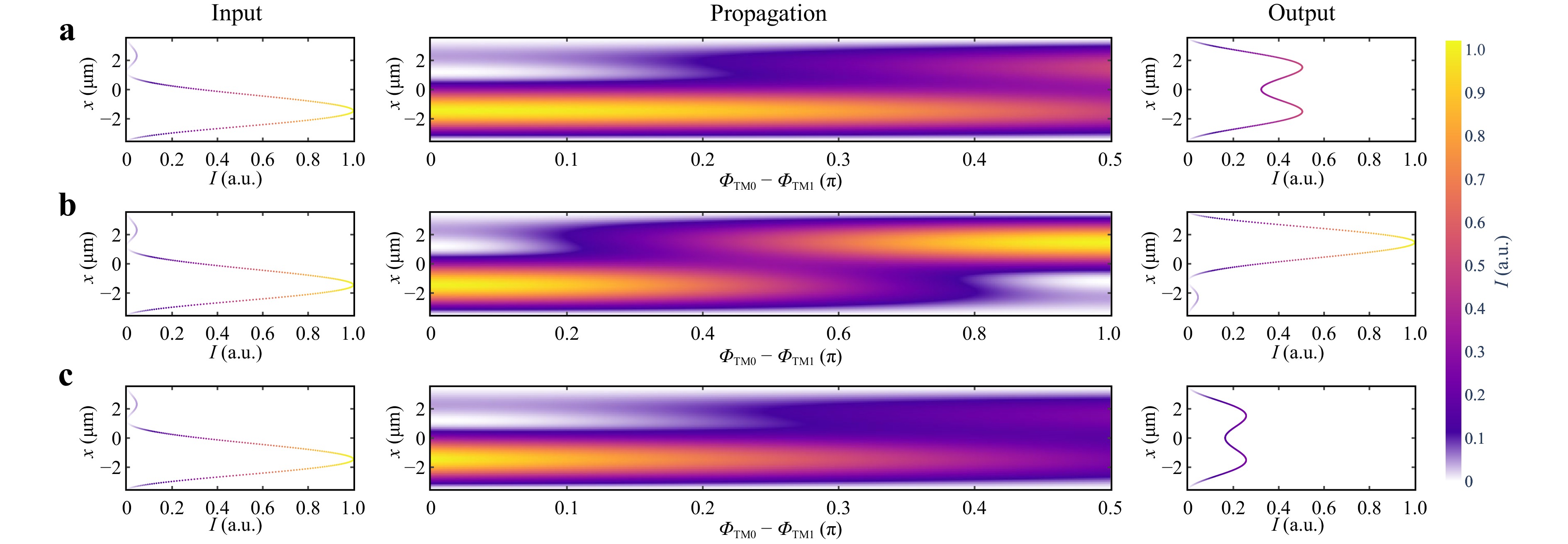
Fig. 1 Intensity distribution of simultaneous TM0 and TM1 mode propagation in a 7 µm-wide waveguide: a without modulation, b with an intermodal phase difference of π/2 due to the propagation, and c with equal attenuation applied to both modes.
In this example, the attenuation coefficients are $ {a}_{0}={a}_{1}=0.001 $. The propagation constants used in the calculations are as follows: for case (a) $ {\beta }_{0}=8100292\;{m}^{-1} $ and $ {\beta }_{1}=8062816\;{m}^{-1} $; for case (b) $ {\beta }_{0}=8139799\;{m}^{-1} $ and $ {\beta }_{1}=8062816\;{m}^{-1} $; and for case (c) $ {\beta }_{0}=8100292+ 8100j\;{m}^{-1} $ and $ {\beta }_{1}=8062816+8063j\;{m}^{-1} $. These cases illustrate three distinct intermodal interactions without considering any real modulators.
The modulator model must incorporate the properties of the ACL in the TCO material. Three approaches are commonly used to describe the ACL: a uniform electron distribution within the expected region, classical drift–diffusion equations, and the quantum moment method19. The modulation properties strongly depend on the ACL thickness. The quantum approach predicts an ACL thickness of approximately 2 nm19. In this study, the charged layer is assumed to have a uniform electron concentration and an effective thickness of 2 nm.
The ACL parameters were determined based on measurements of a 20 nm-thick ITO film using ellipsometry and Hall-effect techniques. The electron concentration in the ITO is approximately $ 2.64~\times {10}^{20} $ cm−3, which is below the epsilon-near-zero (ENZ) concentration of $ 6.45~\times {10}^{20} $ cm−3 at a wavelength of 1552 nm. The permittivity as a function of electron concentration was calculated using the Drude model Eq. 231.
$$ \epsilon \left(\omega \right)={\epsilon }_{\infty }-\frac{\omega _{p}^{2}}{{\omega }^{2}+{\gamma }^{2}}+i\frac{\gamma \omega _{p}^{2}}{\omega \left({\omega }^{2}+{\gamma }^{2}\right)} $$ (2) In Eq. 2 $ {\epsilon }_{\infty } $ is the high-frequency permittivity, $ {\omega }_{p} $ is the plasma frequency, and $ \gamma $ is the relaxation rate. These parameters are given by:
$$ {\omega }_{p}=\sqrt{\frac{N{e}^{2}}{{\epsilon }_{0}{m}^{*}}} ,\quad \gamma =\frac{e}{\mu {m}^{*}} $$ (3) In this work, the parameters $ {m}^{*}=0.35\;{m}_{e} $ and $ {\epsilon }_{\infty }=3.9 $ were used. The electron mobility $ \mu $ was measured to be approximately 38 cm2/(V · s). Substituting this value into Eq. (3) yields $ \gamma =1.62e+14\;{s}^{-1} $. The calculated permittivity changes from (2.304 + 0.220i) in the unbiased state to (0 + 0.538i) at the ENZ condition.
Fig. 2 presents the results of three-dimensional finite-difference time-domain (FDTD) simulations of the modulator structure (Fig. 3), considering excitation by the TM0 and TM1 modes. The simulations compare the passive state (without an ACL; blue curves) and the active state (with a 2 nm ENZ ACL; red curves). Fig. 2a, b show the amplitude distributions of the vertical electric field component Ey along the x-axis for TM0 and TM1 excitation, respectively. Fig. 2c, d present the corresponding phase distributions. A horizontal line monitor was positioned at the centre of the waveguide, 700 nm beyond the active modulation region. Both amplitude and phase modulation effects are observed, with distinct responses for different modes (Fig. 2). Consequently, similar output field distributions can be achieved by adjusting the input conditions through transverse displacement. The dependence of modulation behaviour on the excited mode is essential for achieving the desired inversion of modulation within a single waveguide.
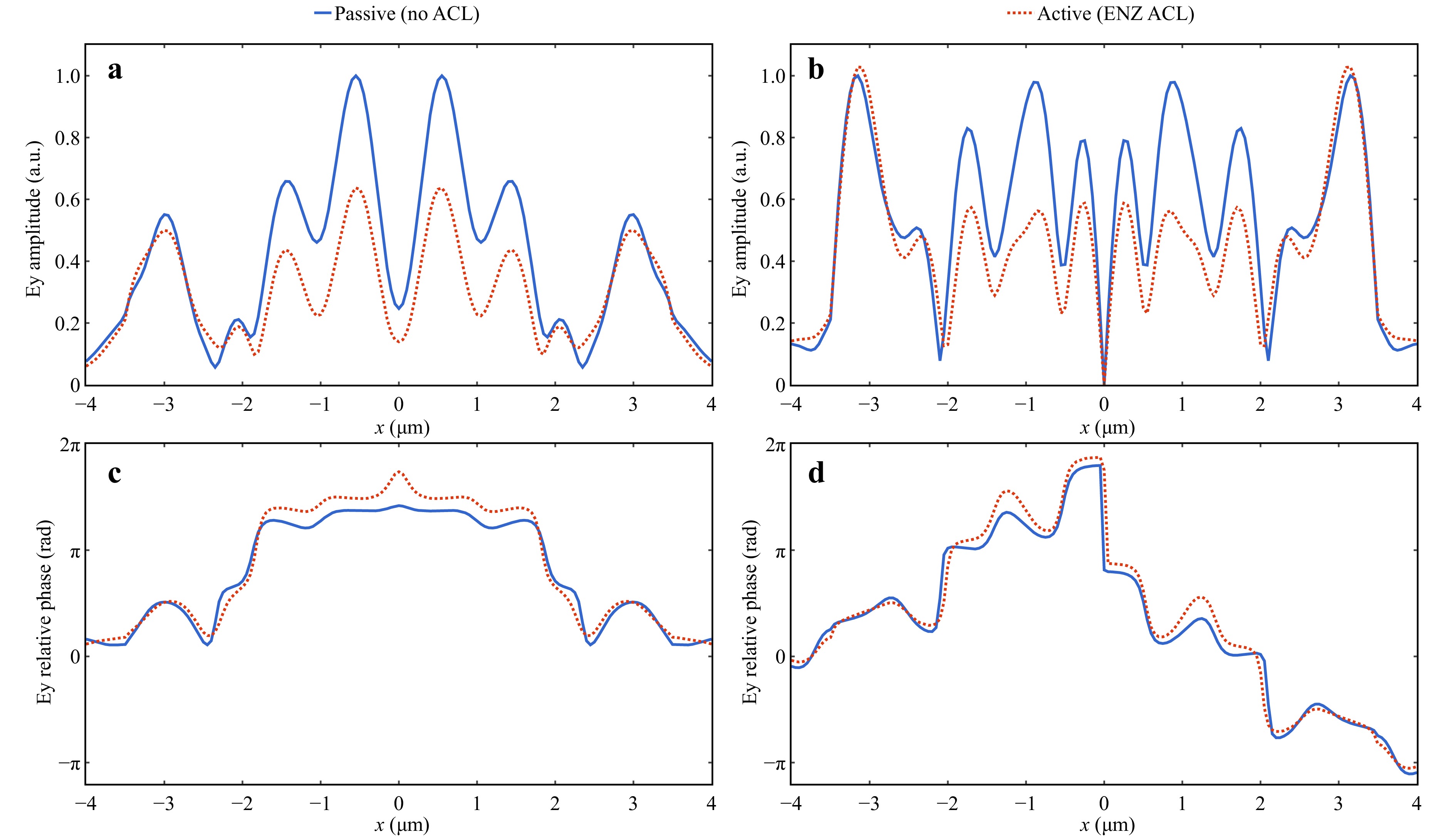
Fig. 2 FDTD simulation results for output fields with TM0 a, c and TM1 b, d excitation. Blue curves represent the passive regime no ACL, uniform electron concentration of 2.64 × 1020 cm−3, while red curves correspond to the active regime with a 2 nm ENZ ACL, with electron concentration of 6.45 × 1020 cm−3.
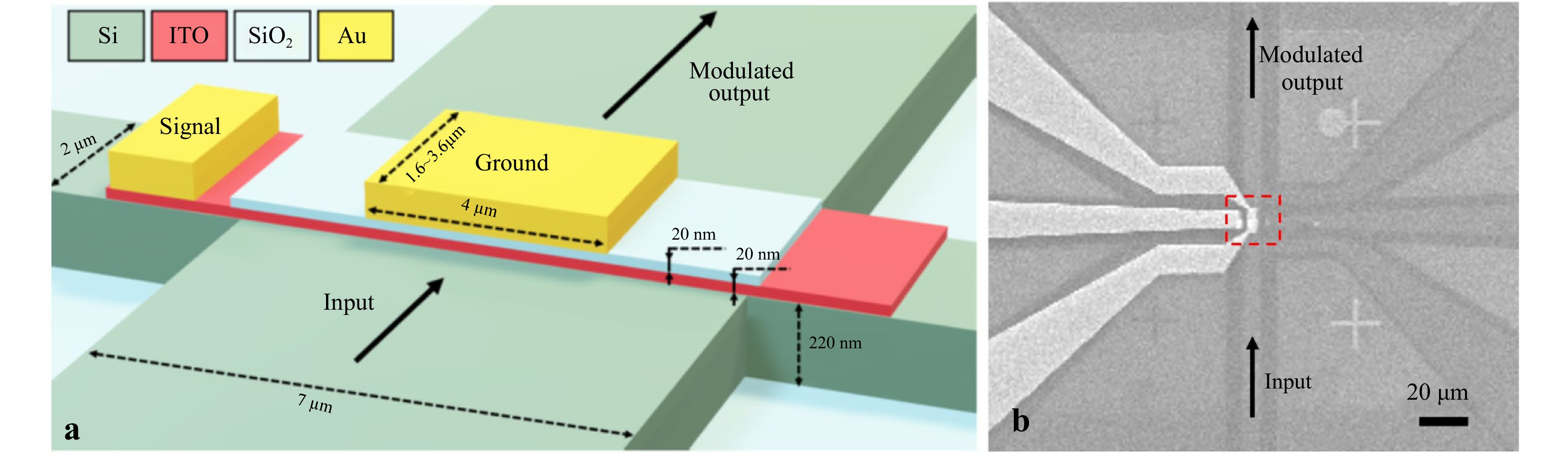
Fig. 3 a Schematic of the proposed modulator. b SEM image of the fabricated structure, with the modulation region highlighted.
-
A “crossroad” design was employed to connect the central contact of the ground-signal-ground (GSG) configuration to the modulator via an ITO film deposited on a planar silicon surface (Fig. 3). This approach eliminates the need for contact transitions across the Si/SiO2 interface trench.
The integrated multimode plasmonic modulators were fabricated on a silicon-on-insulator (SOI) wafer with a 220 nm-thick silicon layer and a 2 µm-thick buried oxide (BOX) layer. The fabrication process followed a standard flow, including electron-beam lithography, inductively coupled plasma (ICP) etching, and electron-beam deposition, all compatible with large-scale manufacturing. Electron-beam lithography was carried out using a scanning electron microscope (SEM; JEOL JSM-7200F) equipped with a Xenos XPG2 pattern generator. Selective plasma etching of the silicon layer was performed using a CSAR AR-P 6200 (Allresist) resist mask in a PlasmaPro 100 (Oxford Instruments) system with SF6 and CHF3 gases. Following waveguide etching, the surrounding regions were filled with SiO2 via electron-beam deposition using a NexDep Ångström vacuum deposition system. The ITO/SiO2/Au capacitor was then fabricated on the silicon waveguide using electron-beam lithography, deposition, and a lift-off process. Each capacitor layer was deposited using the same vacuum deposition system. The capacitor dimensions were 4 µm in width and either 1.6 µm or 3.6 µm in length. The ITO layer thickness was 20 nm, while the SiO2 layers were each 20 nm thick. Previous studies have demonstrated good performance for modulators employing 20 nm-thick ITO layers14,16,21. Additionally, a 30 nm ITO layer may offer improved material quality compared with thinner films. The following section presents measurement results primarily for structures with a 20 nm-thick ITO layer, with selected results for 30 nm also included. The TM-mode input and output GCs, fabricated with shallow etching, were defined on the silicon waveguides using electron-beam lithography and plasma etching. The etching depth of the TM GC was 85 nm, with a period of 1100 nm and a gap of 200 nm. The GC design followed the method described in32. In these experiments, the coupling efficiency of the TM GC was approximately −3 dB.
The measurement setup comprised an analogue optical link. Continuous-wave laser light (Thorlabs TLX1) at a wavelength of 1.55 µm was coupled into the input GC via a lensed optical fibre probe (FormFactor LWP) and collected at the output GC using a similar probe (Fig. 4). The sample was mounted on a FormFactor MPS150 probe station equipped with precision positioners, enabling controlled excitation of different waveguide modes and spatial sampling across the GC. The modulation signal was applied to the device via a 50 GHz GSG Z-probe. The modulated optical signal was amplified using an erbium-doped fibre amplifier (EDFA; Keopsys CEFA-C-HG). The optical link terminated at a PD (Finisar XPDV2150R) with a 50 GHz bandwidth and 0.53 A/W sensitivity. The optical power was adjusted to approach the maximum input level tolerated by the PD (+10 dBm), which remained an order of magnitude below the maximum EDFA output. Link characteristics were measured using a vector network analyser (VNA; Keysight N5224A). A high-resolution optical spectrum analyser (BOSA 440) was used to observe modulation sidebands. Due to the complex nature of the modulation, the output signal was also analysed using a Tektronix MDO3012 oscilloscope with a 200 MHz bandwidth and a sampling rate of 2.5 GSa/s. In addition, several experiments were conducted to measure the DC ER using the same laser source, a DC voltage supply, and a power meter (Thorlabs S155C).
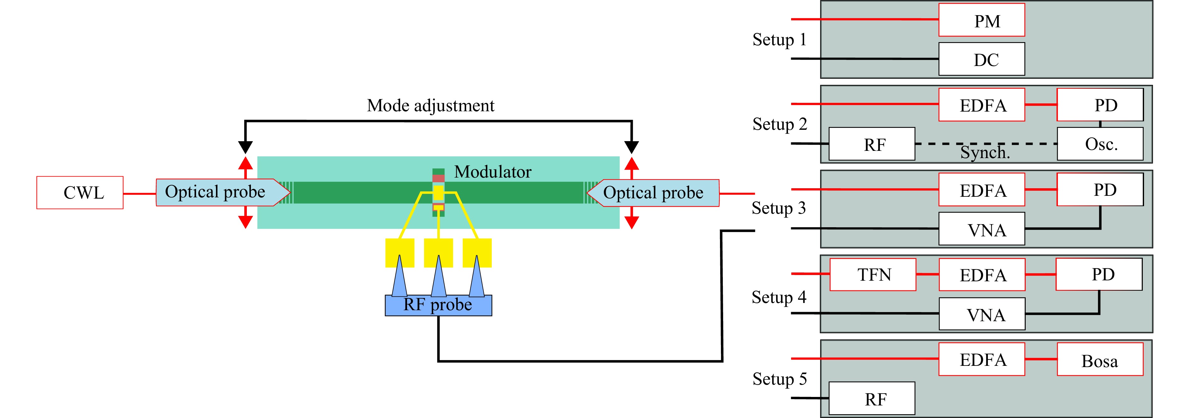
Fig. 4 Measurement configurations used to characterise the integrated modulator. Red lines indicate optical paths and black lines electrical connections. CWL: continuous-wave laser; TFN: tunable ultra-narrowband optical notch filter; EDFA: erbium-doped fibre amplifier; PD: photodetector; VNA: vector network analyser; PM: power meter; DC: DC source; RF: radio-frequency source; Osc: oscilloscope; BOSA: high-resolution optical spectrum analyser. Setup 1: DC extinction ratio measurement; Setup 2: time-domain analysis of the analogue optical link for phase verification and direct AC ER measurement; Setup 3: S21 characterisation of the optical link; Setup 4: verification of pure phase and pure amplitude modulation states; Setup 5: optical spectrum analysis of modulation sidebands.
-
The key characteristics of the proposed structure are presented in Fig. 5. Analysis of the multimode modulator revealed two distinct alignment regimes: one corresponding to maximum optical transmission and the other to maximum modulation extinction (Fig. 5a). These regimes are characterised, respectively, by high transmission with a low ER, and reduced transmission with a high ER. Both regimes were achieved by adjusting the positions of the optical fibre probes across the GC. High-frequency measurements were performed using a VNA with Setups 3 and 4 (Fig. 4). Initially, the S21 parameter was measured with the probes aligned for maximum optical transmission. Under these conditions, the transmission of the structures reached approximately −3.5 dB, while the corresponding S21 value was about −55 dB.
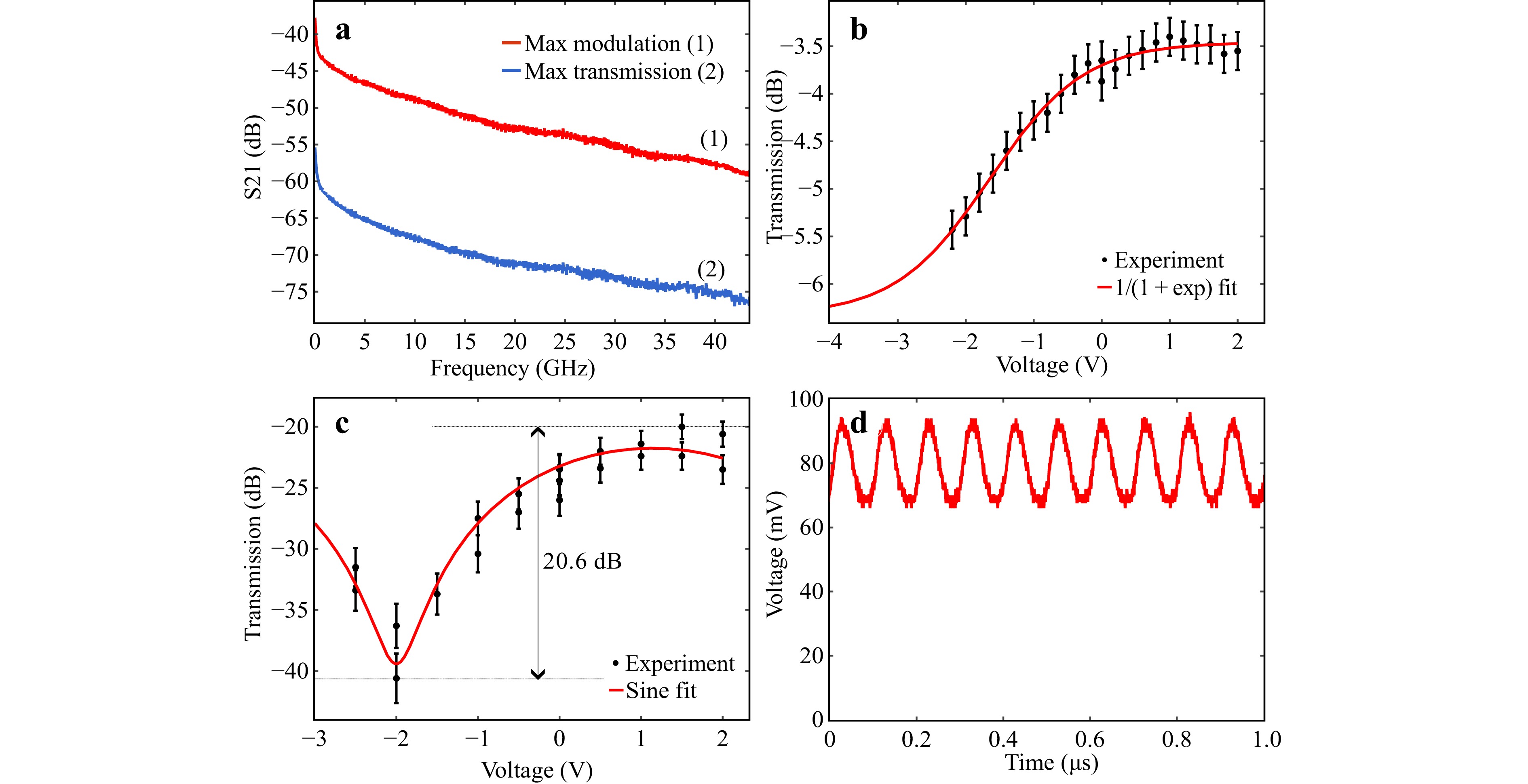
Fig. 5 a S21 response of the analogue optical link with a 3.6 µm-long modulator (20 nm ITO) for two alignment regimes: maximum modulation (red curve) and maximum transmission (blue curve); b measured (points) and sinusoidally fitted (red curve) DC ER for the 1.6 µm-long modulator in the maximum transmission regime (ER > 2 dB); c measured (points) and exponentially fitted (red curve) DC ER for the 1.6 µm-long modulator in the maximum modulation regime (ER = 20.6 dB); d output waveform of the analogue optical link with the 3.6 µm-long modulator in the maximum modulation regime at 10 MHz under +16 dBm RF input.
Subsequently, optimisation based on the S21 response rather than transmission resulted in a significant improvement, with S21 increasing to approximately −38 dB. Each probe exhibited two positions corresponding to local maxima in S21; however, one position consistently provided values a few decibels higher than the other, in agreement with oscilloscope measurements. The S21 response for the 3.6 µm-long structure is shown in Fig. 5a, comparing probe positions corresponding to maximum transmission (blue curve) and maximum S21 (red curve).
Following S21 characterisation, the ER was measured in both DC and AC regimes. As expected, the DC ER differed significantly between the maximum transmission and maximum modulation states. DC measurements were performed using Setup 1 (Fig. 4). For the 1.6 µm-long device, the ER exceeded 2 dB in the maximum transmission regime (Fig. 5b) and reached over 20 dB in the maximum modulation regime (Fig. 5c). Notably, both measurements required several minutes to stabilise.
To investigate high-speed modulation performance, time-domain measurements were conducted at 10 MHz using an oscilloscope (Setup 2, Fig. 4). Fig. 5d shows the output waveform of the analogue optical link for the 3.6 µm-long modulator operating in the maximum modulation regime under a +16 dBm RF input signal. The spontaneous emission from the EDFA was evaluated using an optical spectrum analyser and a power meter by subtracting the optical carrier power from the total amplified signal power during modulation. The total measured optical power was 6.6 mW, comprising approximately 3.6 mW from the laser carrier and 3 mW from spontaneous emission. The measured ER at 10 MHz was approximately 1.33 dB (Fig. 5d). After correcting for spontaneous emission, the ER increased to 2.46 dB, representing the intrinsic modulation performance of the device.
The S21 parameter is related to the ER as well as other system parameters; therefore, the ER can be derived from measured S21 values. The S21 parameter and ER are defined as:
$$ S_{21}=\frac{{P}_{RFout}}{{P}_{RFin}} $$ (4) $$ ER=\frac{{P}_{OPTmax}}{{P}_{OPTmin}} $$ (5) Here, PRFin and PRFout denote the input and detected RF powers at a given frequency, respectively, whereas POPTmax and POPTmin represent the maximum and minimum optical powers during modulation. Assuming a quadratic response of the PD, the output RF power can be expressed as33:
$$ {P}_{RFout}={Z\left(S\frac{{P}_{OPTmax}-{P}_{OPTmin}}{2\sqrt{2}}\right)}^{2} $$ (6) where Z = 50 Ω is the load impedance and S = 0.53 A/W is the PD responsivity. The difference POPTmax − POPTmin can be expressed in terms of the average output optical power POPT and ER:
$$ {P}_{OPTmax}-{P}_{OPTmin}=2{P}_{OPT}\frac{ER-1}{ER+1} $$ (7) Therefore, the output RF power can be expressed as:
$$ {P}_{RFout}={0.5Z\left(S{{P}_{OPT}}\frac{ER-1}{ER+1}\right)}^{2} $$ (8) For an ER of 2.46 dB and a useful optical power of 3.6 mW (excluding spontaneous emission), the calculated RF output power is PRFout = −21.6 dBm. This is consistent with the experimentally measured S21 value of −37.8 dB at 10 MHz for an input RF power of PRFin = +16 dBm. Knowing the parameters of the system and rearranging the above expressions allows the ER to be calculated directly from the measured S21:
$$ ER=\frac{S {P}_{OPT}\sqrt{Z}+\sqrt{2{P}_{RFin}{S}_{21}}}{S {P}_{OPT}\sqrt{Z}-\sqrt{2{P}_{RFin}{S}_{21}}} $$ (9) Using this relation, the ER at 1 GHz is calculated to be approximately 1.25 dB.
As probe displacement across the GC results in different modulation regimes, additional measurements were performed at intermediate probe positions. The ER was evaluated in the time domain using an oscilloscope (Setup 2, Fig. 4) for various optical probe positions across the GC. These positions correspond to different combinations of TM waveguide modes. The resulting oscillograms are presented in Fig. 6a. These measurements confirm the existence of two positions corresponding to maximum modulation extinction. These positions approximately correspond to the simultaneous excitation of the TM0 and TM1 modes with comparable power. The waveforms measured at these two positions exhibit a phase shift of π with high accuracy. The two π-shifted positions are spatially separated by approximately 2.5 µm, as determined through numerical analysis of optical microscope images. This observation is consistent with the results obtained for the 1.6 µm-long structure with a 20 nm ITO layer. During these measurements, synchronisation from the VNA was used to trigger the oscilloscope. Therefore, it was necessary to verify the phase behaviour independently of any artificial temporal alignment.
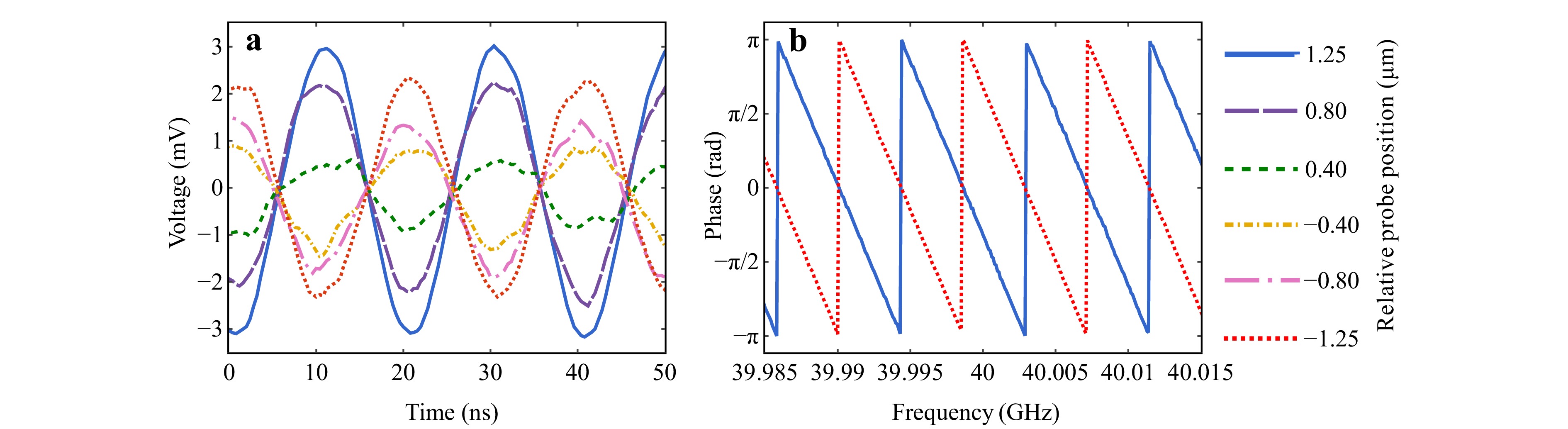
Fig. 6 a Output waveforms of the analogue optical link with a 3.6 µm-long modulator for different output fibre probe positions across the GC; b phase–frequency response of the same system for two probe positions corresponding to maximum modulation. Different colours represent different probe positions across the GC, with values indicating displacement from the waveguide centre.
Using the VNA, the π phase shift between signals at opposite GC positions was also confirmed at high modulation frequencies. An example at 40 GHz is shown in Fig. 6b. The phase–frequency response demonstrates that signal inversion persists across the entire measurable frequency range, up to 43 GHz.
The −3 dB S21 bandwidth of modulators with a 20 nm ITO layer is relatively limited, whereas devices with a 30 nm ITO layer exhibit improved bandwidth uniformity (Fig. 7a). The 30 nm ITO structure demonstrates a −3 dB bandwidth of approximately 13.4 GHz; however, its maximum S21 value is lower than that of the 20 nm ITO modulator. The measured DC ER for the 30 nm device is approximately 1 dB, and an ER of 0.26 dB at 1 GHz is extracted from the S21 response. Overall, the performance of modulators with a 30 nm ITO layer is inferior across the measured frequency range up to 43 GHz. This degradation is attributed to increased optical losses associated with the thicker ITO layer. Specifically, the measured electron concentration in the 30 nm ITO film is approximately twice that of the 20 nm film. The higher initial carrier concentration leads to increased insertion loss and reduced ER, as the ACL thickness does not significantly depend on the total ITO thickness.
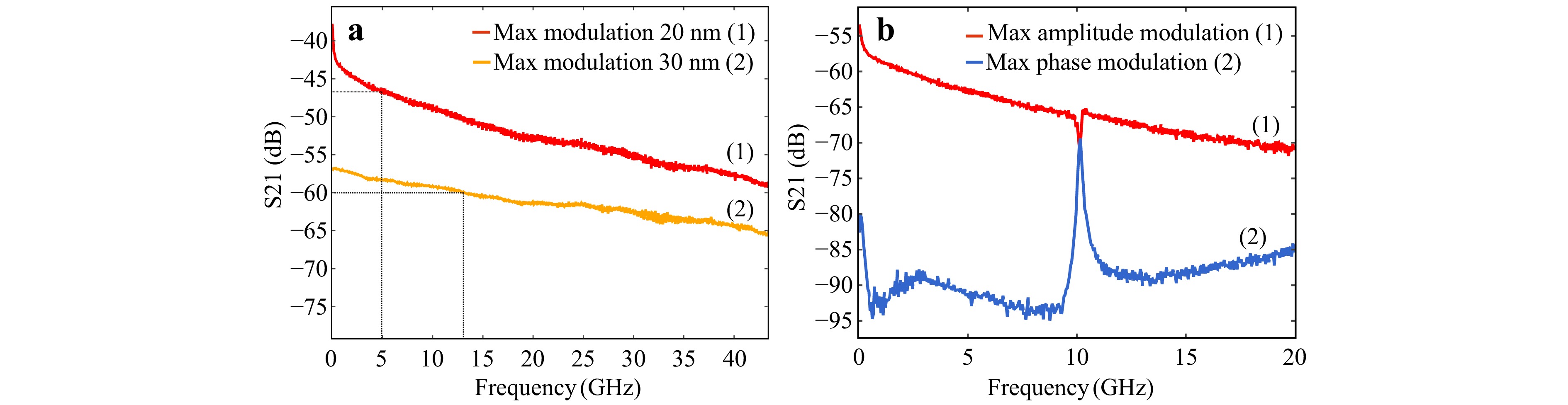
Fig. 7 a S21 response of the analogue optical link with a 1.6 µm-long modulator for 20 nm (red) and 30 nm (yellow) ITO layers; the dashed line indicates the −3 dB bandwidth (5 GHz for the structure with a 20 nm ITO layer and 13.4 GHz for the structure with a 30 nm ITO layer); b S21 response of the 3.6 µm-long modulator (20 nm ITO) with a notch filter inserted. The red curve corresponds to maximum amplitude modulation, and the blue curve to maximum phase modulation.
The analysis of modulation behaviour (Fig. 2) suggests that certain spatial positions favour either phase or amplitude modulation. In general, aside from interactions between even and odd modes, amplitude modulation is expected to dominate at the output. However, when only a single mode is excited, electro-refractive effects may result in predominantly phase modulation. Fig. 7b presents the S21 response of the analogue optical link with a Teraxion TFN ultra-narrowband optical notch filter (bandwidth ~100 MHz) inserted between the integrated modulator and the EDFA (Setup 4, Fig. 4). The conversion of phase modulation to amplitude modulation through selective suppression of modulation sidebands in the optical domain is well established34. This effect has also been utilised in tunable optoelectronic oscillators based on phase modulators35. When amplitude modulation dominates, the notch filter introduces a small dip in the S21 spectrum by suppressing one sideband. In contrast, when the modulation is mostly phase-based, suppression of a harmonic leads to phase-to-amplitude conversion, resulting in a peak at the frequency corresponding to the difference between the laser carrier and the notch filter. Achieving these distinct modulation regimes requires precise adjustment of the probe positions.
Finally, the optical spectrum of the integrated Si–ITO HPWG modulator, including modulation sidebands, was measured and is reported here for the first time (Fig. 8). These measurements were obtained near the probe position corresponding to maximum modulation. The amplitudes of the modulation sidebands are in good agreement with the frequency-domain ER measurements, although they exhibit only weak correlation with the DC ER values.
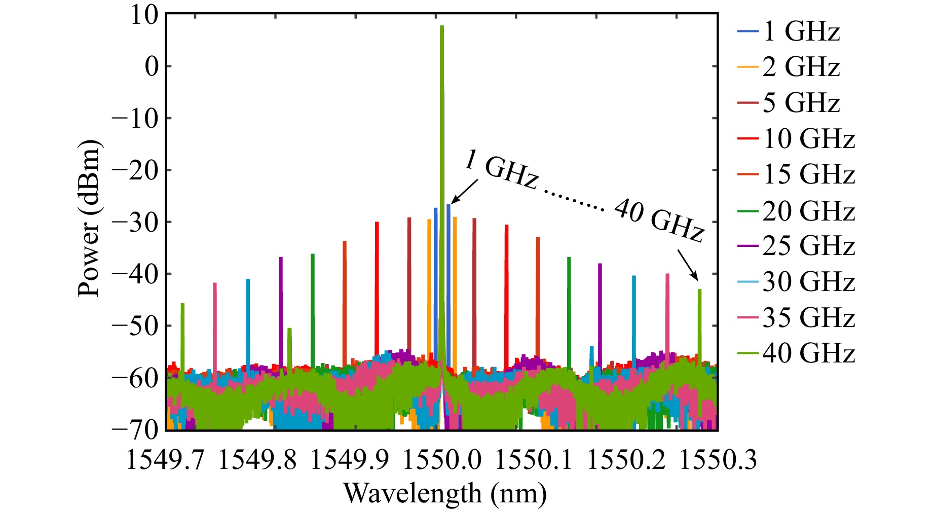
Fig. 8 Optical spectrum of the integrated modulator showing modulation sidebands.
-
In addition to its robust design, the multimode modulator exhibits complex behaviour that reveals novel modulation mechanisms in plasmonic structures based on TCOs. Maximum modulation extinction is observed when both input and output probes are displaced from the centre of the waveguide by approximately 1.25 µm. Excitation of the dominant TM1 mode requires a larger off-centre displacement of approximately 1.75 µm, whereas the fundamental TM0 mode is preferentially excited when the probes are aligned with the waveguide centre. These observations indicate that maximising the modulation effect relies primarily on multimode interference, alongside other contributing mechanisms. Furthermore, the experimentally observed π phase shift is consistent with interference between the symmetric TM0 mode and the antisymmetric TM1 mode.
The numerical results presented in Fig. 1a, b demonstrate that the position of the zero-intensity point at the output shifts due to differential phase modulation of the TM0 and TM1 modes. Exceptionally high ERs can therefore be achieved by carefully controlling the relative modal contributions at the input. This behaviour explains the high DC ER observed experimentally. In previously proposed designs, such as photonic crystals36, MZIs22, and ring resonator37 structures, achieving low output intensity at the modulation minimum requires precise control and compensation of optical losses in the modulator structure. A passive ballast on the MZI arm may even be required. Fabrication tolerances further complicate these approaches. In contrast, the present structure enables post-fabrication tuning of the modal composition through fibre probe positioning, allowing exceptionally high ER per unit length.
A key application of the proposed multimode modulator is in photonic integrated circuits employing balanced detection. Fig. 9 presents oscillograms of inverted output signals (red and blue traces) obtained from the integrated modulator. These measurements were performed using Setup 2 (Fig. 4), with a filter applied to suppress a significant portion of the amplified spontaneous emission. In Fig. 9a, the probe positions were adjusted to maximise the AC modulation depth, whereas in Fig. 9b, they were configured to equalise the DC components of the signals while maintaining a finite ER.
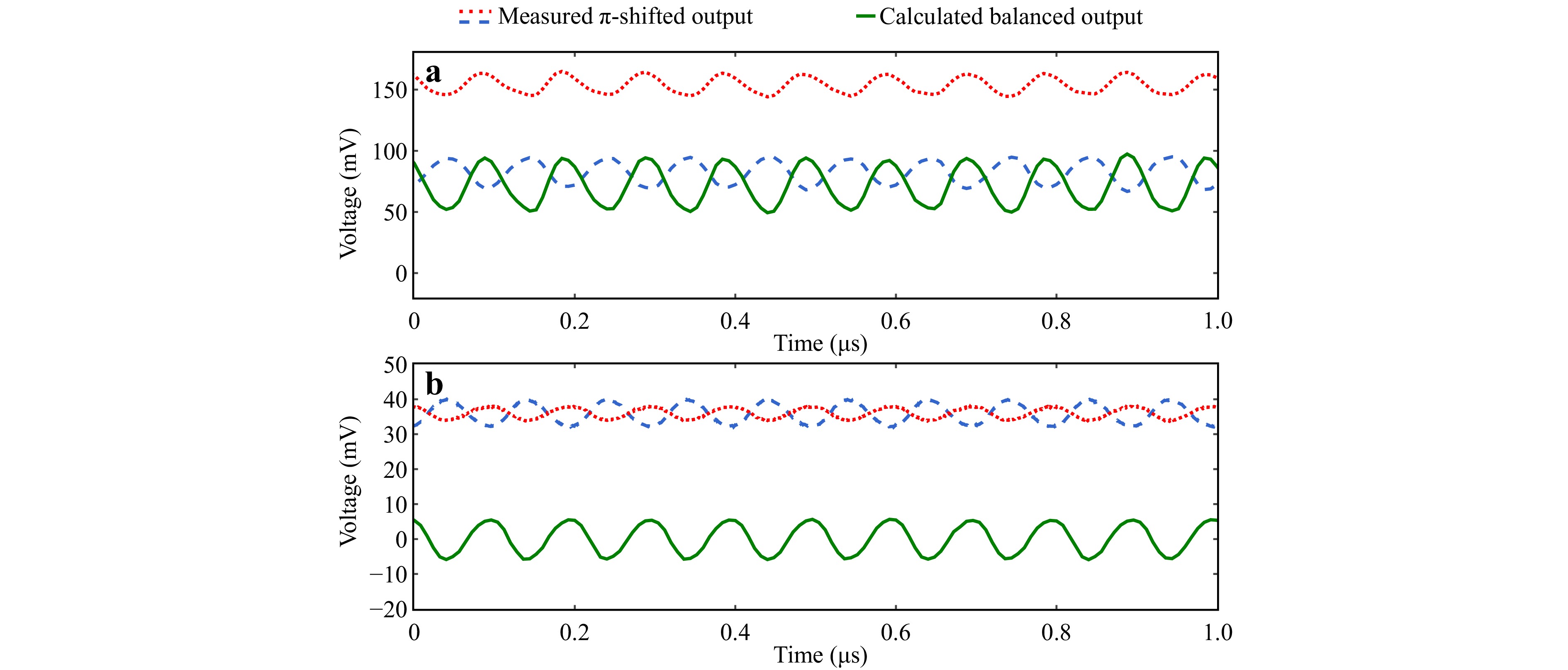
Fig. 9 Output π-shifted signals (red dots and blue dashed lines) of the ITO-based plasmonic multimode modulator measured at two positions on the GC, and their calculated difference (green solid line), representing balanced detection: a maximum modulation depth; b equalised DC offset.
During the experiment, the oscilloscope was triggered by the rising edge of a 10 MHz reference signal from the generator, and the trigger settings were kept constant throughout. In Fig. 9a, the input probe remained fixed, while the output probe was positioned at two locations corresponding to displacements of ±1.25 µm from the GC centre. In Fig. 9b, the input probe position was unchanged, while the output probe was shifted away from the optimal modulation positions to achieve equal DC levels. The recorded traces are presented without temporal alignment or amplitude normalisation, reflecting the raw measurement data.
The green trace in Fig. 9 represents the difference between the two signals (i.e. their mathematical subtraction), simulating the response of balanced detection if implemented in our link. In Fig. 9a, the resulting differential signal exhibits a modulation depth of 47 mV, approximately equal to the sum of the individual signal amplitudes. However, due to modal interference effects, the DC levels differ, resulting in a residual DC offset in the differential signal. The tunability of the modulator enables operation at conditions where the DC components are equalised while preserving the phase difference. Accordingly, in Fig. 9b, the DC component of the differential signal is significantly suppressed, while the amplitude of the balanced signal is increased.
The modulator exhibits a notable difference between DC and AC extinction characteristics. While ER is traditionally determined from DC measurements, this approach is not fully applicable to plasmonic ITO-based modulators , as also noted in Ref. 27. Although structures with bandwidths exceeding 13 GHz, and even above 40 GHz14, have been demonstrated, they typically show significantly higher ER in DC measurements, particularly when evaluated after prolonged voltage application. The DC extinction of over 20 dB observed in this work cannot be directly correlated with the AC extinction. Specifically, the 1.6 µm device exhibits a DC ER of 20.6 dB, corresponding to a record value of 12.8 dB/µm. However, direct AC measurements yield 2.46 dB at 10 MHz and 1.25 dB at 1 GHz. These results indicate that DC ER values cannot be directly extrapolated to high-frequency operation in ITO-based devices.
It is likely that the DC and high-speed modulation mechanisms differ. The high-speed response is associated with modulation of free electron concentration in the ACL, whereas the DC behaviour may involve additional effects. Two mechanisms are therefore expected: a fast response related to electron dynamics, typical of TCO-based modulators, and a slower process, possibly associated with ion migration and electrochromic effects28,38. This suggests that ER measurements without frequency dependence may not fully characterise device performance.
Accurate measurement of RF extinction enables direct comparison with other high-frequency metrics, such as the S21 response of the analogue optical link. In previous studies, S21 is often normalised to 0 dB at DC. In the present multimode design, the interaction area between the optical field and the accumulation layer is increased, enhancing the ER. As a result, modulation sidebands are clearly observable in the optical spectrum, and their amplitudes are consistent with the ER obtained from frequency-domain measurements. Furthermore, calculations based on the optical spectrum and photodetector characteristics yield S21 values that agree with experimental results within approximately 1 dB, confirming the consistency of the RF measurements.
-
This study demonstrates the advantages of the proposed multimode design for a Si-TCO hybrid plasmonic modulator. Multimode interference introduces an electro-refractive modulation mechanism in addition to the absorptive contribution, with the electro-refractive effect identified as the dominant mechanism. The intermodal phase difference generates an interference pattern at the output GC, featuring two spatially separated points with a frequency-independent π phase shift. These points are separated by approximately 2.5 µm within a single waveguide structure, eliminating the need for a bulky MZI configuration. This behaviour enables the generation of complementary signals suitable for balanced routing. In balanced detection schemes, such signals can significantly enhance extinction contrast. By varying the relative contributions of different waveguide modes, the modulation characteristics can be continuously tuned. In particular, both amplitude and phase modulation depths can be adjusted at spatially distinct locations on the output GC. The 1.6 µm-long modulator achieves a DC ER exceeding 20 dB at the optimal modulation position. However, the build-up of the DC ER occurs over relatively long timescales. In contrast, the measured AC ER is 2.46 dB at 10 MHz and 1.25 dB at 1 GHz. These results indicate that DC and AC modulation regimes in ITO-based devices cannot be directly correlated. To the best of our knowledge, prior studies on integrated ITO- or In2O3-based modulators have not provided sufficient data to enable even approximate estimation of AC ERs. Furthermore, the optical spectra of the Si-ITO HPWG modulator clearly exhibit modulation sidebands. These spectral features are in excellent agreement with both calculated and experimentally measured frequency-domain characteristics of the device.
-
This work was supported by the Russian Science Foundation (grant #25-72-31023).
Advantages of multimode Si-ITO electro-optical modulators for balanced signal routing
- Light: Advanced Manufacturing , Article number: 67 (2026)
- Received: 24 November 2025
- Revised: 13 April 2026
- Accepted: 14 April 2026 Published online: 21 May 2026
doi: https://doi.org/10.37188/lam.2026.067
Abstract: An ultra-compact silicon photonic solution based on a multimode plasmonic modulator is proposed for signal processing with complementary routing. The Si-ITO-SiO2-Au structure investigated in this study reveals previously unexplored mechanisms for signal management. In this modulator, both intensity and phase modulation can be selectively achieved. By controlling mode excitation, electro-refraction can be effectively converted into variations in multimode interference. As a result, a single-output grating coupler exhibits two spatially separated regions with inverted intensity modulation. Moreover, the modulation depth at these locations can be readily tuned. The measured DC extinction ratio over a voltage range of −2 to 1.5 V reaches 20.6 dB for a 1.6 µm-long modulator, corresponding to a record-high value of 12.8 dB/µm. The directly measured AC extinction ratio is 2.48 dB at a modulation frequency of 10 MHz, decreasing to 1.25 dB at 1 GHz over a voltage range of −2 to 2 V for a 3.6 µm-long modulator. These results demonstrate a significant step towards the integration of compact, high-speed, and reconfigurable analogue optical links for advanced signal processing.
Rights and permissions
Open Access This article is licensed under a Creative Commons Attribution 4.0 International License, which permits use, sharing, adaptation, distribution and reproduction in any medium or format, as long as you give appropriate credit to the original author(s) and the source, provide a link to the Creative Commons license, and indicate if changes were made. The images or other third party material in this article are included in the article′s Creative Commons license, unless indicated otherwise in a credit line to the material. If material is not included in the article′s Creative Commons license and your intended use is not permitted by statutory regulation or exceeds the permitted use, you will need to obtain permission directly from the copyright holder. To view a copy of this license, visit http://creativecommons.org/licenses/by/4.0/.

 DownLoad: