




-
Encryption plays an important role in mobile communication networks, the Internet of things, and other modern communication systems because information security is indispensable for safely transmitting large amounts of data every day1,2. This imposes a higher demand on the devices in terms of both security and performance. Optical encryption has emerged as a promising strategy3–5. However, conventional optical-encryption technologies remain limited in terms of flexibility and adaptability at the hardware level. Silicon-based encryption devices still struggle to achieve high sensitivity6, low power consumption7, and dynamic encryption capability8. In particular, binary-state operations restrict the modulation diversity and limit the implementation of adaptive encryption schemes9,10. These challenges have motivated the exploration of alternative device platforms capable of multi-state operation.
Owing to their high carrier mobility and strong electrical tunability, two-dimensional van der Waals (vdW) heterostructures provide a versatile platform for advanced optoelectronic devices11–13. This enables the dynamic control of the photo-response. Simultaneously, weak interlayer coupling facilitates heterogeneous integration with CMOS-compatible circuits14,15. Band alignment engineering further allows the effective suppression of the dark current, improving both the on-off ratio and signal-to-noise performance. Because of these advantages, various modulation strategies have been explored. These strategies include gate voltage control16, polarisation-sensitive response17, and multi-wavelength excitation18, as well as multi-state photodetectors based on stacked structures or interfacial engineering. However, several of these approaches rely on complex external components or multiple light sources, whereas others require a relatively high operating bias. Such requirements increase the system complexity and limit the scalability. Consequently, achieving a compact, low-power, and intrinsically reconfigurable device that supports multi-state operations and secure optical encoding remains a significant challenge.
Yu et al. have recently demonstrated a dual-mode vdW phototransistor based on a PtTe2/WS2 heterostructure19. The schematic of the PtTe2/WS2 vdW device is shown in Fig. 1a, in which the optical response can be reconfigured by tuning the bias. This bias-controlled operation enables the transition between the photoconductive (PC) and photovoltaic (PV) modes within a single device. In the PC regime, carrier trapping prolongs carrier lifetime and leads to a large photo-gain, yielding a responsivity of up to 1.37 A·W−1. In contrast, the PV regime is governed by a widened depletion region that suppresses dark current and promotes fast carrier separation, resulting in a high specific detectivity of 9.42 × 10¹⁴ Jones and a response time on the order of tens of microseconds (rise time ~26.3 μs, fall time ~22.6 μs). The ability to switch between these two mechanisms allows the device to combine high sensitivity and fast operation20.
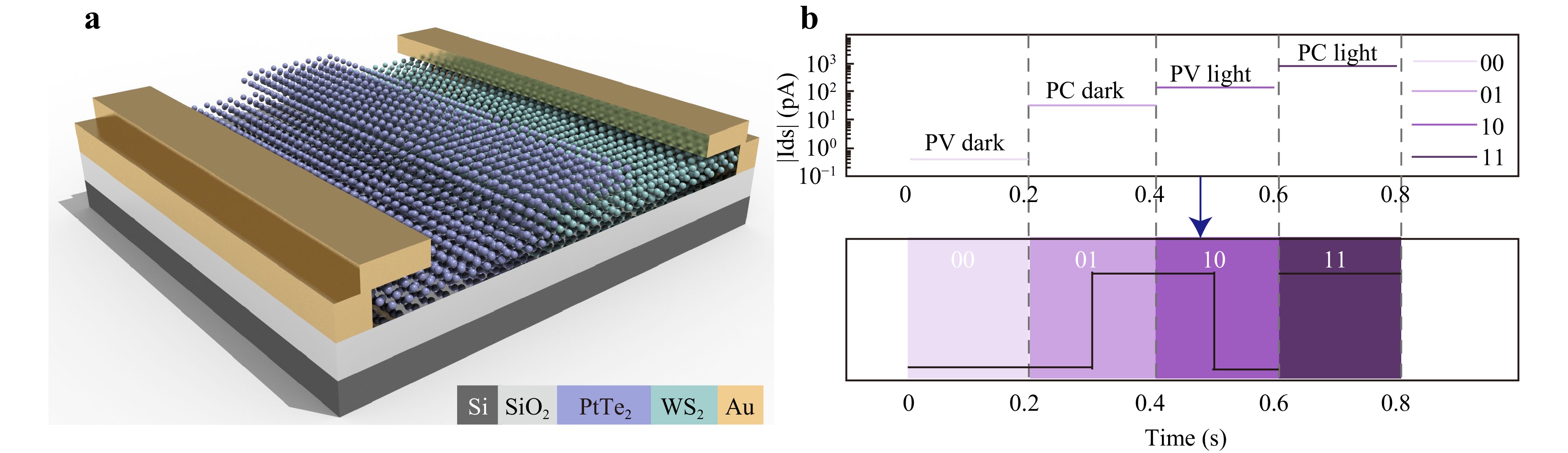
Fig. 1 a Schematic of PtTe2/WS2 dual-mode switchable vdW phototransistor. b Different current levels generated by dual-mode phototransistor and the corresponding quaternary numbers. “00” and “10” represent the dark and source–drain currents under light illumination in the PV mode, whereas “01” and “11” indicate the dark and source–drain currents under light illumination in the PC mode19.
Beyond the performance metrics, a key advancement in this study lies in the generation of four current states from a single device. By using light illumination and bias polarity as independent inputs, the phototransistor moves beyond conventional binary operation and enables multi-level signal encoding with an on-off ratio approaching 105. As illustrated in Fig. 1b, these four states can be mapped to the binary pairs 00, 01, 10, and 11. This mechanism allows the direct translation of image information into sequences of electrical signals through controlled light modulation and bias switching. The resulting sequences can be reconfigured into encrypted outputs according to predefined rules, thereby providing a hardware-level route for multi-state image encryption. This approach highlights how simple physical inputs can be leveraged to achieve complex information-processing functionalities within a single photonic device.
This multi-state functionality enables the implementation of optical logic operations, including XNOR, XOR, and NOR, by directly linking physical inputs to logical outputs. Thus, the device bridges optoelectronic response and information processing within a unified platform. The availability of multiple current levels also improves the robustness of signal discrimination compared with conventional binary systems. Consequently, the device could perform multi-state image encryption with an average adjacent-pixel correlation coefficient as low as 0.03, demonstrating enhanced security and reduced data redundancy at the hardware level.
This study highlights a broad direction for optical encryption and integrated photonic systems. Instead of relying on external modulation schemes or complex system architectures, functional diversity can be achieved through intrinsic device physics and reconfigurable operations. The reported energy consumption at the femtojoule level further underscores the potential for low-power applications21. This demonstration of multi-state reconfigurable photonic encryption represents an important step towards developing more versatile, energy-efficient, and secure optical communication technologies.
Reconfigurable multi-state photonic encryption
- Light: Advanced Manufacturing , Article number: 85 (2026)
- Received: 09 May 2026
- Revised: 14 May 2026
- Accepted: 19 May 2026 Published online: 20 July 2026
doi: https://doi.org/10.37188/lam.2026.085
Abstract: A bias-switchable van der Waals phototransistor demonstrates reconfigurable transitions between photovoltaic and photoconductive modes, generating four current states within a single device. This multi-state functionality advances on-chip optical logic and image encryption. It offers a promising route towards secure, low-power, and highly integrated photonic communication systems.
Rights and permissions
Open Access This article is licensed under a Creative Commons Attribution 4.0 International License, which permits use, sharing, adaptation, distribution and reproduction in any medium or format, as long as you give appropriate credit to the original author(s) and the source, provide a link to the Creative Commons license, and indicate if changes were made. The images or other third party material in this article are included in the article′s Creative Commons license, unless indicated otherwise in a credit line to the material. If material is not included in the article′s Creative Commons license and your intended use is not permitted by statutory regulation or exceeds the permitted use, you will need to obtain permission directly from the copyright holder. To view a copy of this license, visit http://creativecommons.org/licenses/by/4.0/.

 DownLoad: