






-
Terahertz (THz) waves possess potential applications in security imaging, radar stealth, biomedicine, and 6G communications1−6. Meanwhile, the development of flexible, broadband, low-cost, and large-area components in optical systems has gained importance with the rapid development of functional THz devices. To meet these requirements, various polymer substrates have been explored for flexible THz devices, such as polyethylene terephthalate (PET), polydimethylsiloxane, and polyimide7−10. Among them, PET offers a practical balance among optical transparency, low cost, moisture resistance, dimensional stability, and roll-to-roll compatibility, which are favourable for flexible THz optoelectronic devices11,12. The elastic deformability of flexible PET substrates make these THz devices suitable for irregularly shaped surfaces and complex measurement situations that require embedding in curved surfaces, thereby enabling applications in wearable photonic healthcare devices, flexible photodetectors, and chemical and biological sensors7−13.
However, flexible all-optical THz modulators face significant challenges in achieving both high performance and mechanical robustness. In practical scenarios, most existing flexible devices undergo structural changes induced by mechanical deformation14−21, and fail to meet the stability requirements of communication or imaging applications under arbitrary bending conditions. From the material perspective, current flexible all-optical THz modulators based on two-dimensional (2D) nanofilms face a trade-off between modulation depth and speed19−26. Therefore, a novel material with superior photoresponse and mechanical stability is urgently required. As a narrow direct band gap semiconductor, tellurium (Te) nanofilms have attracted extensive interest owing to their excellent optical properties, high carrier mobility, and good ambient stability27−29. Notably, Te is consists of atomic chains in a triangular helix, which are stacked together via van der Waals forces in a hexagonal array and possess a one-dimensional (1D) crystal structure28,30. Owing to this unique helical chain configuration, Te nanofilms exhibit exceptional mechanical flexibility and high strain tolerance and withstand structural deformation without fracture. Hence, Te nanofilms integrated with flexible substrates are ideal candidates for realising flexible high-performance devices with excellent mechanical robustness.
In this study, we present an all-optical THz modulator based on Te/PET films, which exhibits good flexibility and bending stability. Time-resolved THz spectroscopy measurements revealed that the Te-based device with broadband and low insertion loss achieved a high modulation depth of 50% on the picosecond timescale and an ultrasensitive response under low pump excitation. In addition, the proposed THz modulator exhibited high tolerance to bending deformation, and the transient photoresponse remained almost unchanged even after 1,000 bending cycles or at a bending radius of 3 mm. Furthermore, an artificial neural network (ANN) was constructed for static image processing. The recognition rate based on the Modified National Institute of Standards and Technology (MNIST) handwritten database reached 95%, and the variation range under different bending conditions was only 2%, which was nearly the same order of magnitude as the fluctuation caused by the neural network during the training process. This study provides the foundation for the development of flexible THz-functional devices and offers a promising strategy for establishing next-generation intelligent optoelectronic systems.
-
High-quality and large-area Te nanofilms were deposited by the electron beam evaporation method on PET substrates with thickness of 15 µm. To further confirm the crystal structures of the different domains, high-resolution transmission electron microscopy (HRTEM) was performed (Fig. 1a), which directly illustrated the crystalline state of the Te layer with a thickness of approximately 100 nm. In the bottom of Fig. 1a, the HRTEM images of a cross-section along the c-axis reveal a clear atomic matrix with three-fold symmetry, where each atomic triangle represents a single helical chain. Moreover, the lattice spacing is 0.32 nm from the (101) plane. The Raman spectra are shown in Fig. 1b. The prominent peaks located at 93, 122, and 141 cm−1 are attributed to the E1, A1, and E2 vibration modes, which originate from asymmetric bond-stretching along c-axis and are assigned to bond-bending, chain expansion, and bond-stretching types, respectively28. As shown in Fig. 1c, the X-ray photoelectron spectroscopy (XPS) spectrum of the Te nanofilm exhibits two obvious peaks with the binding energies of 573.5 and 583.8 eV, which are assigned to Te 3d5/2 and Te 3d3/2, respectively29−31. Fig. 1d illustrates the schematic of the experiment, which uses optical pump-THz probe (OPTP) technology to investigate the active modulation response and mechanical features of Te-based THz devices.
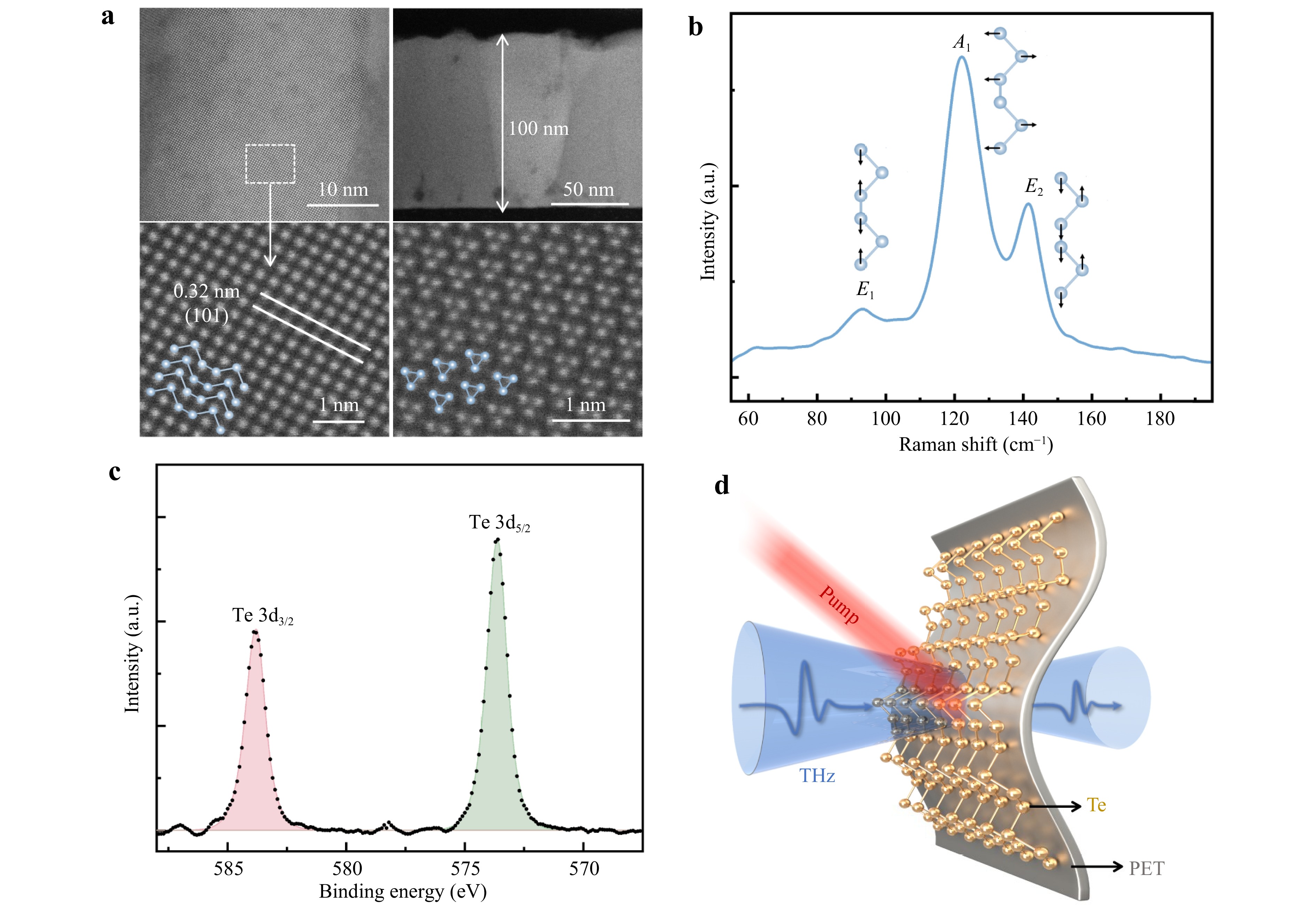
Fig. 1 Material preparation and characterization. a HRTEM images, b Raman spectrum, and c XPS spectrum of Te nanofilms. d Schematic of the THz measurement scheme.
-
The measured transient THz dynamics for Te/PET with 800 nm pump excitation are shown in Fig. 2a. The transient THz dynamics of the bare PET substrate exhibit no modulation after photoexcitation, demonstrating that the THz modulation observed in this study originates solely from the Te nanofilm. The relative change is quantified by the modulation depth MD, which is defined as a function of the pump delay time t: MD(t) = −ΔT/T0 = −(T − T0) /T0, where T0 and T represent the peak THz amplitude before and after the photoexcitation, respectively. The device exhibits a rapid rise in MD, reaching its maximum within several picoseconds upon photoexcitation, which is attributed to the generation of hot carriers32,33. The subsequent relaxation processes under different pump fluences are satisfactorily fitted by biexponential functions, and the extracted relaxation times τ1 and τ2 are displayed in Fig. 2b. The fitting function $ y={A}_{1}{e}^{-\frac{x-{x}_{0}}{{\tau }_{1}}}+{A}_{2}{e}^{-\frac{x-{x}_{0}}{{\tau }_{2}}} $ is used, where τ1 and τ2 are the time constants, while A1 and A2 are the corresponding amplitudes, respectively. The fitting parameters were determined based on the physical timescales of the observed decay processes. The decay consists of two stages with distinct timescales. The fast decay τ1 is due to the energy relaxation of the carriers, while the slow decay τ2 depicts the lifetime of the carriers34. Fast recovery occurs within 2.5 ps, which represents the energy relaxation of the carriers. This pump-independent trend of τ1 is attributed to electron-phonon scattering35. The slow recovery that lasts for approximately 8.5 ps depicts the carrier lifetime, and its independence of pump fluence suggests that synergistic interactions between the Auger effect and defect trapping dominate the photocarrier dynamics of Te nanofilms29,35. The recombination centres formed by impurities and defects promote recombination and shorten the carrier lifetime, whereas the formation of the trap centre prolongs the lifetime. This feature aids in attaining unperturbed modulation speed in optical active devices because the carrier lifetime usually deteriorates with increased pump intensity. The MD(t = 0) of Te is 5.5%, even at an extremely low power of 1 mW, and reaches 50.8% at 100 mW, while the corresponding transmission spectra at a pump delay time of 0 ps exhibit fluence-dependent, but frequency-independent broadband features (Supplementary Fig. S1). The high transmission of this material (approximately 96.1% without the pump) leads to a very low insertion loss of −0.35 dB calculated by 20lg (Esam/Esub), where Esam and Esub are the THz amplitudes for the sample and substrate, respectively. Fig. 2c presents a comprehensive performance comparison between the Te/PET device and other flexible THz modulators based on 2D nanomaterials (see Table S1 for details)14−26. For instance, VO2-based devices exhibit high MD within milliseconds. Conversely, modulators with graphene (Gr) or Ge, which exhibit ultrafast picosecond responses, possess limited modulation efficiencies. The Te/PET device presented in this work successfully attained optimal indices with a high MD of 50.8% and an ultrafast picosecond response in current flexible nanofilm components, suggesting a potential modulation speed of tens of GHz range. These parameters are relevant to communication and imaging applications. Specifically, high modulation ensures reliable amplitude encoding; picosecond response time corresponds to potential high-speed modulation capability; while low insertion loss and broadband response guarantee efficient signal transmission with minimal distortion.
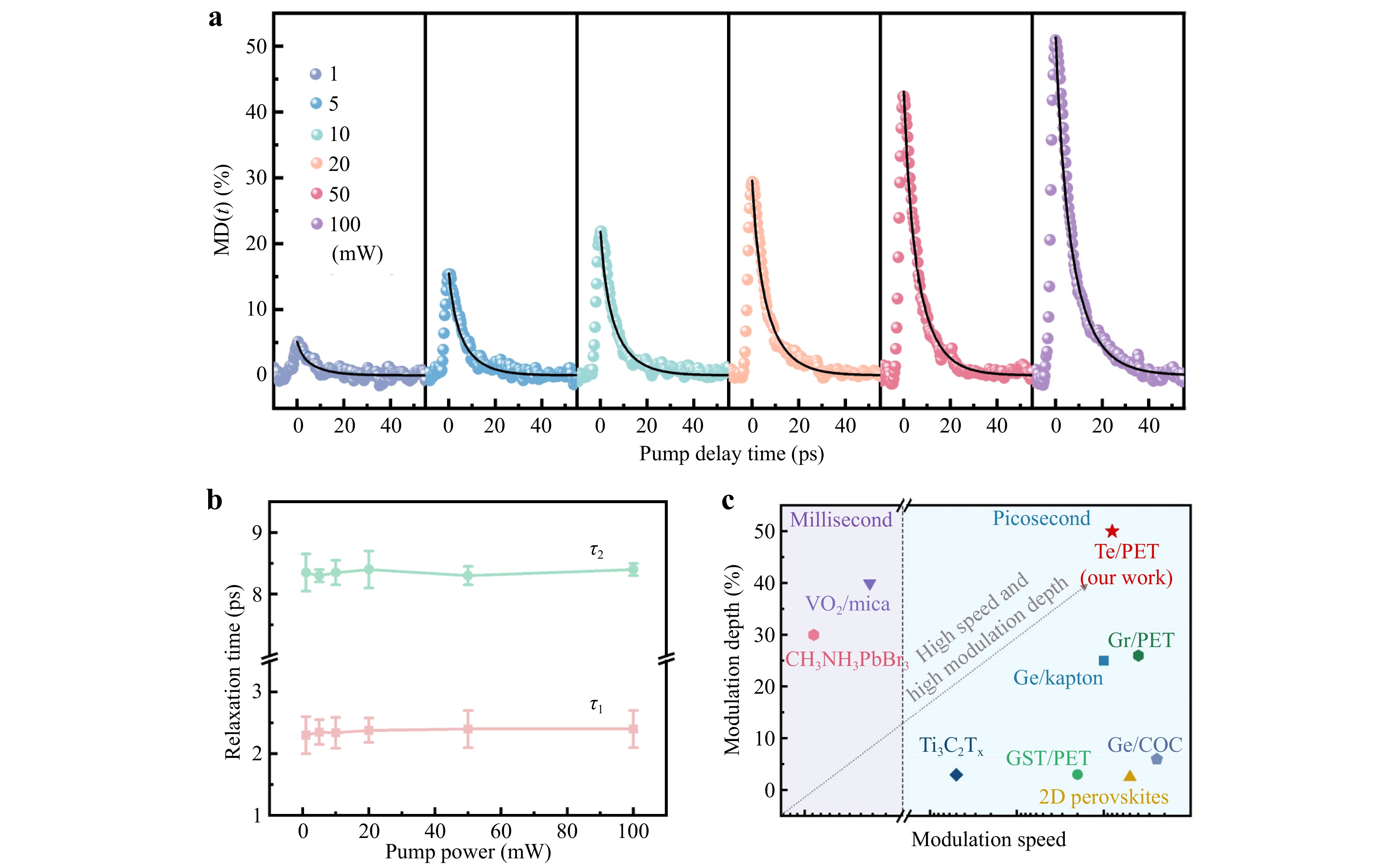
Fig. 2 Transient dynamics properties of Te/PET. a Transient THz dynamics of Te/PET under different pump powers at an excitation wavelength of 800 nm. The black solid lines represent the biexponential fitting curves. b Pump power dependence of the fitted relaxation times. c Performance comparison of optical flexible THz modulators among the 2D nanofilms.
-
As shown in Fig. 3a, we first examined the photoresponse stability of the device in the flat state after 1000 illumination cycles (on/off = 1/1s) at a pump power of 20 mW and delay time of 0 ps. MD remains constant without degradation, indicating excellent durability and reproducibility. These results reflect the operational stability of the device performance under repeated optical excitation and can serve as a baseline test for communication or imaging systems. In this mapping, the optically controlled off and on states correspond to digital 0 and 1 in THz communication or low- and high-intensity pixels in imaging applications. The unchanged THz modulation depth after 1,000 on/off cycles indicates excellent robustness and demonstrates that the device operates stably under both high-frequency and long-term working conditions. In addition, the Te/PET films exhibited excellent spatial uniformity and long-term ambient stability, ensuring the robustness of the device (Supplementary Figs. S2, S3). We further studied the transient THz dynamic properties of the flexible Te nanofilms under various bending conditions at the same pump power. During these measurements, the flexible Te/PET device was fixed on a copper bar and bent to any state. Fig. 3b presents the experimental results under bending deformation with radii of 8, 5, and 3 mm. We then examined the bending cyclability for 100, 500, and 1,000 times with a bending radius of 6 mm, as shown in Fig. 3c. The transient THz dynamics curves of the Te nanofilm do not exhibit obvious variations under different bending radii and cycles compared to those in a flat state. The modulation performance remained stable even after 10,000 bending cycles (Supplementary Fig. S4). This excellent mechanical robustness can be attributed to the unique quasi-1D crystal structure of Te27,28. Unlike isotropic bulk crystals, the trigonal Te lattice comprises stacked helical atomic chains spiralling along the c-axis, which are stacked together via weak van der Waals interactions. Under bending deformation, these weak interchain forces allow stress relaxation through slight chain reorientation or sliding to prevent structural fracture27. In addition, the Raman spectra were utilised to investigate the effect of bending states on the lattice structure (Supplementary Fig. S5). The three characteristic vibrational peaks exhibited no obvious shifts, indicating that the Te nanofilm maintained its high structural integrity and original crystalline state without significant lattice distortion during the bending process. The robustness of the Te/PET device was further proved by the small tensile strain of 0.25%, which was considerably less than the strain limit because the tensile strain is the ratio of the whole sample thickness (15.1 µm) to the bending radius (3 mm)36−39. The bending durability is particularly important for flexible devices and is a primary index of device degradation. Therefore, we performed mechanical measurements on the device under different bending radii (8, 5, and 3 mm), as shown in Fig. 3d-f. After 1,000 cycles, the transient photoresponse properties at t = 0 fluctuate negligibly for all bending radii. Furthermore, these key metrics remain nearly unchanged under different bending radii and after repeated bending cycles, indicating that the device maintains stable modulation output even under mechanical deformation and complex physical environments. This robustness against mechanical fatigue further confirms that Te/PET devices are ideal for practical applications.
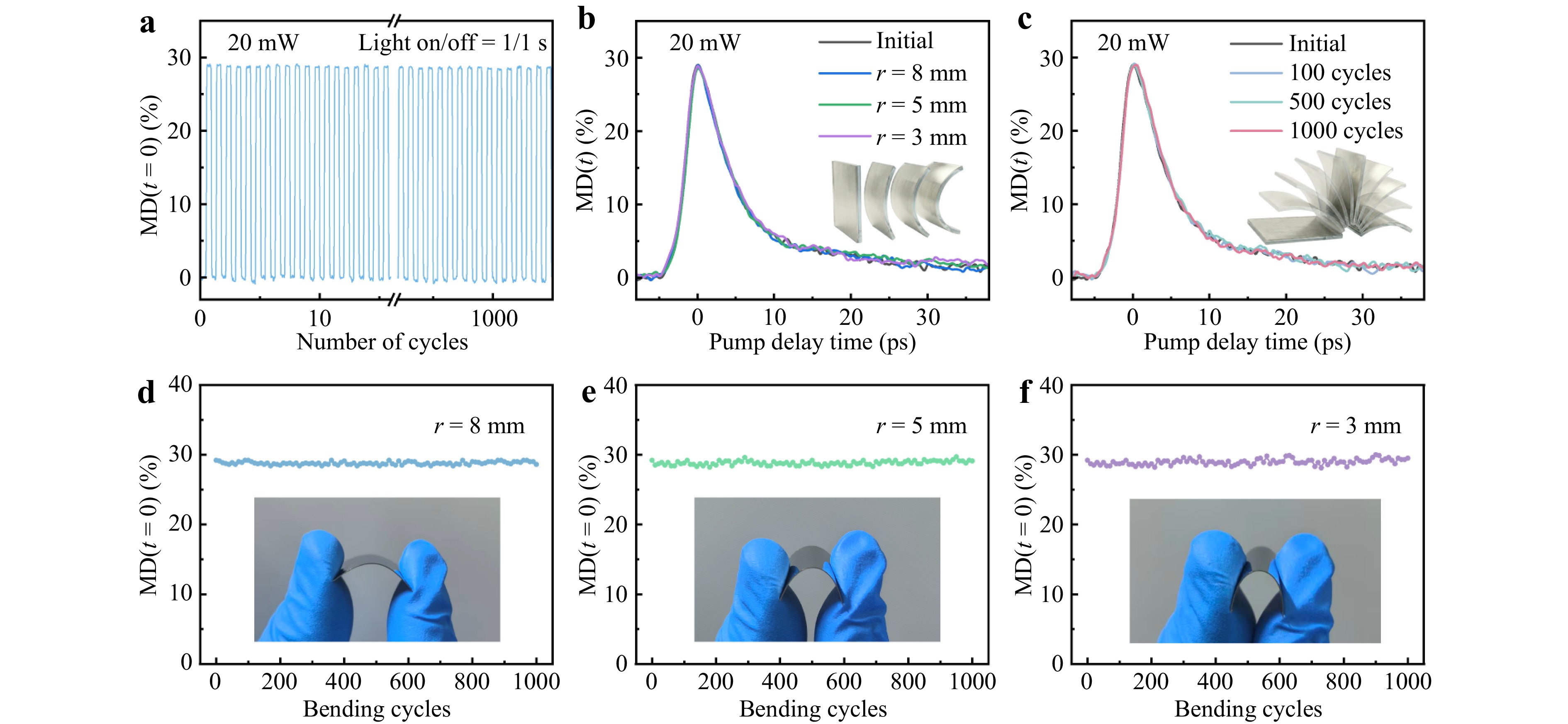
Fig. 3 Mechanical flexibility and durability of device. a Optical switching stability measurement under initial state over 1,000 illumination cycles at pump delay time t = 0. b Transient THz dynamics curves of Te nanofilm under different bending radii (8, 5, and 3 mm) and c for different bending cycles (100, 500, 1,000) at a bending radius of 6 mm. d-f Transient photoresponse properties (t = 0) for 1,000 bending cycles under different bending radii. The insets display photographs of the bending equipment.
-
Unlike conventional devices that often suffer from signal interruption or destruction under mechanical deformation, the proposed device maintains robust information transmission capabilities, as illustrated in Fig. 4a. Fig. 4b shows the potentiation and depression behaviours with incremental light pulses of 3–100 mW under the flat and bending states. The MDs of the devices change regularly with the number of applied pulses. The device states can be reversibly programmed between high and low conductance levels by actively controlling the optical input. The results demonstrate that the device presents a continuously adjustable MD regardless of bending deformation. The photoresponse behaviours in the six bending states are consistent with those in the flat state, confirming the good bending tolerance of the device. In addition, ensuring stable information fidelity under mechanical deformation conditions is essential. The extracted response profiles of the initial and bent states at 5 mm indicated that all the devices maintained an ultrafast response time of approximately 8 ps and preserved symmetric and linear photoresponse features without distortion (Fig. 4c). These characteristics are crucial for the recognition accuracy of simulations. To explore the feasibility of the proposed devices for neuromorphic computing, a typical ANN was established to test the MNIST database. The grey value (0–255) of each pixel in a handwritten digit image was linearly mapped to the THz pump power (0–100 mW), and 784 sensory neurons were used to sense the stimuli and encode them into different MDs. The mapping relationship between the THz pump power and encoded MD is shown in Fig. S6. The input information, MD, was then read as the modulated THz amplitude by the probe pulse and fed into a three-layer ANN consisting of 784 input, 300 hidden, and 10 output neurons for processing. The stimuli images were classified into 10 different categories after training the network. Fig. 4d, e show the evolution of the test accuracy during the training process for the three bending radii and cycles, respectively. The recognition accuracy remains stable at approximately 95% with a variation range of only 2% under the bending conditions after 30 training epochs, which is similar to the fluctuation caused by the neural network itself during training. Fig. 4f shows the confusion matrix of the classification results for 10,000 test images after 30 epochs at a bending radius of 3 mm. The columns designate the actual labels of the stimuli images; the rows represent the inferred results; and the colour bars indicate the number of instances. The confusion matrix for the other bending conditions is shown in Fig. S7. The results verified that the mechanical robustness of the device was effectively translated into high-performance pattern recognition. The conceptual demonstration of pattern classification suggests the proposed flexible device can be used for object recognition, indicating its great potential for use in intelligent optoelectronic devices.
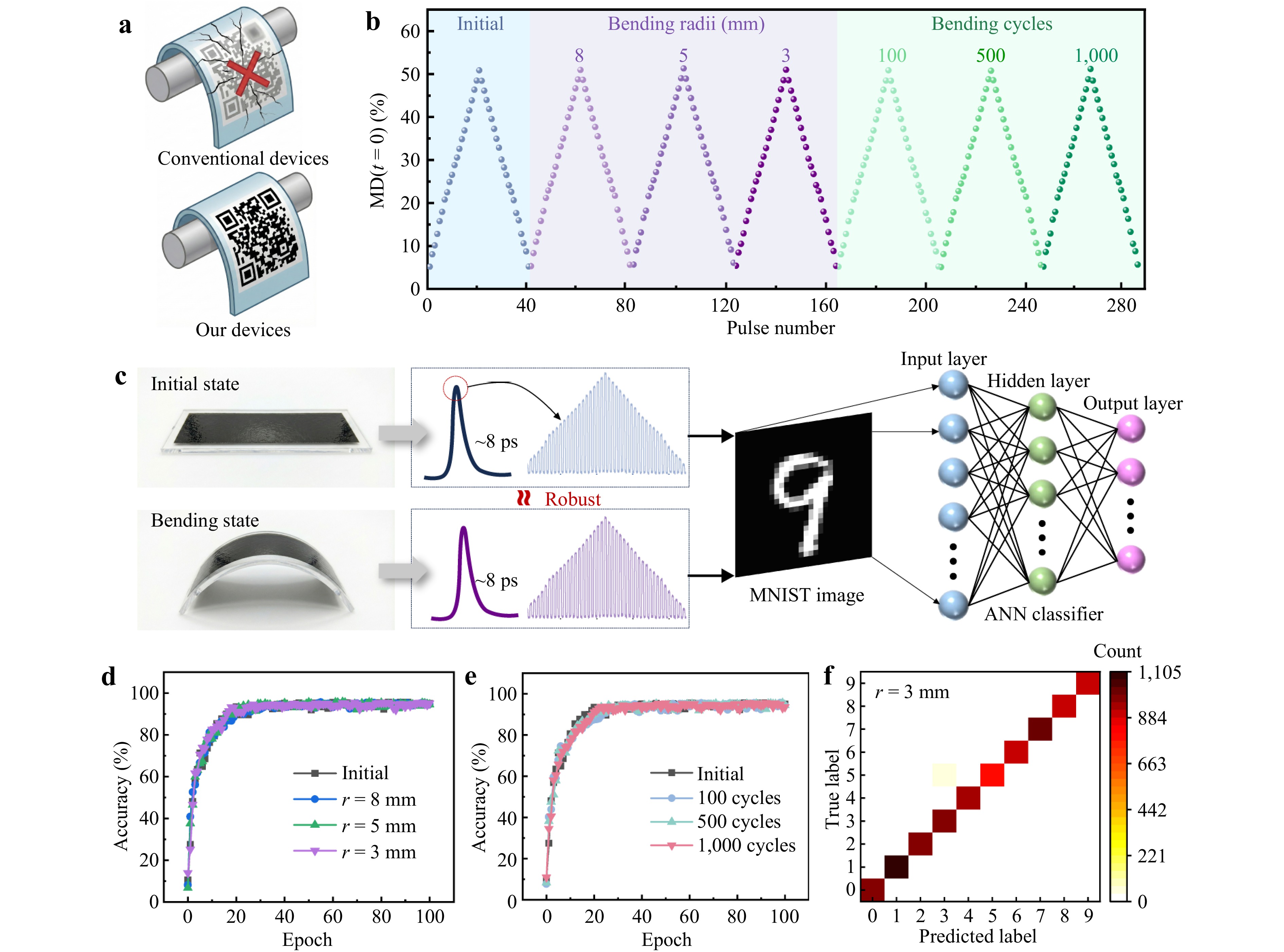
Fig. 4 Application of the flexible Te/PET modulator in neuromorphic computing. a Schematic comparison of the mechanical durability of conventional devices and the proposed Te/PET device. b Measured MD with incremental light pulse under different conditions. c Schematic of the ANN-based image recognition simulation. d Recognition accuracy of the ANN classifier under different bending radii and e after different bending cycles. f Confusion matrix of the classification results of the test dataset after 30 epochs at a bending radius of 3 mm.
-
In summary, we used Te nanofilms on a PET substrate to demonstrate a high-performance flexible and mechanically robust THz modulator. This device achieved optimal indices with a high modulation efficiency (50% MD) and picosecond-level ultrafast speed (8 ps) in existing flexible 2D material systems. Notably, the modulation performance remained unchanged under bending deformation even at a bending radius of 3 mm and 1,000 bending cycles. Furthermore, we constructed an ANN consisting of the proposed devices for static image processing and successfully achieved a recognition function in the THz band. The recognition accuracy of the MNIST handwritten database reached 95%, and the variation range under different bending conditions was only 2%, further demonstrating that the proposed device possessed excellent mechanical stability. Such mechanically robust Te-based THz devices offer a promising solution for efficient pattern-recognition systems and lay the foundation for the development of flexible intelligent optoelectronic devices with neuromorphic functions.
-
The Te nanofilms were grown on PET substrates in an electron-beam evaporator (VZS 600 Pro) with an in situ thickness meter. Before deposition, the PET substrates were cleaned via ultrasonication in acetone for 10 min and rinsed with isopropyl alcohol and deionised water. Te deposition was initiated from a 99.999% pure Te source in a boron nitride crucible at a rate of 0.1 nm·s−1 under 10−4 Pa pressure. Annealing was performed in a tube furnace at 373 K under 100 sccm Ar atmosphere for 0.5 h.
-
HRTEM was performed using a Cs-corrected JEOL JEMARM200CF NEOARM instrument operated at 200 kV with a CEOS Cs corrector (CEOS GmbH, Heidelberg, Germany). Raman spectra were analysed using an alpha300 R microscope under 532 nm laser excitation. XPS measurements were performed on ThermoFisher Scientific ESCALAB 250X under monochromatic Al Kα radiation with energy of 1486.6 eV.
-
The 800 nm source beam with a 100 fs duration and 1 kHz repetition rate delivered by a Spectra Physics regenerative amplifier was divided into three paths to generate THz waves, probe the THz signal, and pump the samples. First, the transmitted THz signals were measured by blocking the pump beam. A 1D pump curve was then obtained by scanning the pump delay line with the THz generation delay line at a fixed position at the peak of the THz pulse. The spot size of the pump beam was approximately 0.3 cm2. In our OPTP measurements, the zero point of the pump delay time was defined as the maximum MD, corresponding to the greatest pump-induced change in the peak THz amplitude. This point represents the time at which the optical pump and THz probe pulses encounter each other in the sample.
-
The ANN combined with a Te-based THz device consisted of an input layer, a hidden layer, and an output layer with 784, 300, and 10 nodes, respectively. The backpropagation algorithm was used for the training process, and the weight update rule was defined using the experimental potentiation and depression data shown in Fig. 4b. The activation functions of the hidden and output layers are Sigmoid and Softmax, respectively.
-
We thank Prof. Cheng-Wei Qiu for the discussions and comments. This study was supported by the National Key R&D Program of China (No. 2024YFA1409500), Postdoctoral Fellowship Program of CPSF (GZC20252257), Beijing Natural Science Foundation (Nos. 4264139 and 4262076), China Postdoctoral Science Foundation (2025M783418), Beijing Postdoctoral Science Foundation (pc-2025-06), National Natural Science Foundation of China (Nos. 62075142 and 12222414), and Youth Innovation Promotion Association of CAS (No. Y2022003).
Flexible and robust Te/PET films for ultrafast all-optical terahertz modulators
- Light: Advanced Manufacturing , (2026)
- Received: 29 December 2025
- Revised: 19 May 2026
- Accepted: 21 May 2026 Published online: 24 July 2026
doi: https://doi.org/10.37188/lam.2026.086
Abstract: Flexible terahertz (THz) devices are fundamental components of wearable photonics and intelligent communication systems. However, conventional THz devices are affected by information loss or signal interruption due to mechanical deformation, which degrade their information fidelity. Here, we introduce tellurium (Te) nanofilms grown on polyethylene terephthalate (PET) substrates as a new class of mechanically robust THz modulators that can successfully improve device performances to optimal levels among existing flexible broadband modulators. The ultrafast transient THz photoresponses of two-dimensional Te films remained unchanged even after 1000 bending cycles or at a small bending radius of 3 mm, exhibiting high tolerance to bending deformation. Furthermore, the variations in the pattern recognition accuracy remained within 2% under different bending conditions, indicating its adaptability to various deformation conditions. This prototype lays the foundation for developing intelligent perception elements that operate stably under complex mechanical deformations.
Research Summary
Flexible and robust tellurium-based terahertz modulators
Flexible tellurium nanofilms enable ultrafast terahertz modulation while maintaining stable performance under mechanical bending. Qingli Zhou from Capital Normal University, Chen Ge from Chinese Academy of Sciences and colleagues now report an all-optical terahertz modulator by growing tellurium nanofilms on polyethylene terephthalate. The device could achieve a high modulation depth of 50% on the picosecond timescale and an ultrasensitive response under low pump excitation. In addition, the proposed THz modulator exhibited high tolerance to bending deformation, and the transient photoresponse remained almost unchanged even after 1000 bending cycles or at a bending radius of 3 mm. Furthermore, pattern-recognition accuracy varied by less than 2% under different bending conditions, indicating its adaptability to various deformation conditions. This prototype lays the foundation for developing intelligent perception elements that operate stably under complex mechanical deformations.
Rights and permissions
Open Access This article is licensed under a Creative Commons Attribution 4.0 International License, which permits use, sharing, adaptation, distribution and reproduction in any medium or format, as long as you give appropriate credit to the original author(s) and the source, provide a link to the Creative Commons license, and indicate if changes were made. The images or other third party material in this article are included in the article′s Creative Commons license, unless indicated otherwise in a credit line to the material. If material is not included in the article′s Creative Commons license and your intended use is not permitted by statutory regulation or exceeds the permitted use, you will need to obtain permission directly from the copyright holder. To view a copy of this license, visit http://creativecommons.org/licenses/by/4.0/.

 DownLoad: