






-
In recent decades, carbon nanotubes (CNTs) have been considered as one of the most studied nanomaterials1. A broad range of properties of CNTs2,3 inspired a variety of diverse applications, starting from electronic nanodevices to bulky composite details and from nanometer-sized sorbents to space elevator cables4. Driven by their potential performance, the scientific and industrial communities invested tremendous resources to gain control over the atomic structure of individual CNTs and their macroscopic assemblies in the form of yarns, films, aerogels, forests, etc. These resulted in the concept of multi-level engineering of carbon nanotube products starting from atomic features and propagating to the macro level5,6.
The formation of CNT patterns can be achieved in situ (during the assembly formation process) or ex situ (i.e., afterwards). For CNT films and forests, laser cutting7, CNC (computer numerical control) milling8, or lithography with subsequent plasma etching9,10 have been proposed. Though the lithography is the only method to reach submicron resolution, the ex situ methods suffer from CNT losses (up to 99%)9 and deterioration of their intrinsic properties, limiting the wide range of potential applications. On the contrary, in situ methods of patterning allow efficient use of CNTs, often preserving their unique properties. For example, inkjet printing, selective vacuum filtration, and spray deposition facilitate the fabrication of patterned electrodes with a resolution of tens of micrometers, though heavily relying on the quality of CNT suspensions and suffering from the presence of surfactant on the surface of CNTs11. Moreover, current advances in the fabrication of CNT suspensions mostly deal with vigorous ultrasound individualization, resulting in the CNT shortening/damage, in turn, limiting the performance of the patterned films.
Alternative dry in situ patterning can be realized either by (1) a spatially tailored catalyst deposition for the further synthesis of forests or individual nanotubes/sub-percolating networks12, or by (2) a controlled film deposition of synthesized aerosol CNTs. For the latter, a membrane for the aerosol filtration can be covered with a resist13, a metal layer14, or a polymer15,16 stencil. Though this facilitated significant progress in transparent electronics15,17 and THz optics18, the materials used for the membrane coverage limit the performance by the thickness, patterning resolution (due to adhesion of the CNTs to the stencil), and by the harsh conditions (e.g., in the presence of NO219).
In the present paper, we combine aerosol CVD synthesis of single-walled CNTs (SWCNTs) with a modified membrane to directly form patterned films in a single step, without the need for additional processing. Unlike other filter modification techniques, our approach does not embed extra material into the filter matrix; instead, it locally alters the membrane structure by pressing specific areas, thereby changing pore density and selectively blocking aerosol flow paths during deposition, enabling SWCNTs to be collected only on the desired regions of the surface. Our approach comes in two modes: a stencil-free variant, where the stencil is removed after the imprinting, allowing for versatile pattern designs, and the stencil-supported variant, where the stencil remains attached to the membrane, enhancing flow blockage at lower imprinting pressures. As a demonstration, we showcase the single-step fabrication of strain sensors and stretchable THz spiral zone plates (SZP). The latter was characterized through direct intensity measurements and correlated with numerical modelling. Fabricated strain sensors in turn match or surpass the performance of existing mechanical sensors based on SWCNTs.
-
SWCNTs were produced using the aerosol CVD method20 (Fig. S1). Ferrocene, which plays the role of precursor for Fe-based catalyst particles, was fed to the quartz tube inside the oven with an isothermal zone length of ca. 700 mm in the atmosphere of carbon monoxide (CO, 99.999%) as described elsewhere21–23. The Boudouard reaction (CO disproportionation; 854 °C) on the catalyst surface results in the release of carbon atoms and subsequent SWCNT nucleation and growth. 1.2 vol% of CO2 was additionally introduced to tune the diameter, length, and defectiveness of the SWCNTs24. At the outlet of the reactor, an aerosol of SWCNTs with a concentration of ca. 106 cm−3 is obtained. Here, we produce exclusively single-walled carbon nanotubes with a low degree of bundling (Fig. S1a) with high quality (Fig. S1b IG/ID ratio=38.4), and an average diameter of 1.5 nm (based on S11 position of UV-vis-spectrum; Fig. S1c). The SWCNTs have a mixed chirality (roughly 67% of semiconducting and 33% metallic; Fig. S1c). When deposited, SWCNTs form randomly oriented uniform networks (thin films, Fig. S1d). For the SWCNT aerosol deposition, Merck Millipore HAWP filter membranes with 0.45 µm pore size were used. The material of membranes, characterized by low adhesion to CNTs, enabled the dry transfer of the collected SWCNT films. The dry transfer technique25 is a powerful tool for fabrication of CNT film deposited on any demanded substrate allowing the films to be suitable stretchable electrodes for various devices: LEDs26, memristors27, sensors28, etc.29,30 The key advantage of the method is the robustness, absence of liquids and any other treatment.
The proposed approach comprises stencil preparation and imprinting (Fig. 1). The imprinting was performed with a Collin p300 p/m machine with a 296 × 296 mm2 area and 300 kN maximum force at 250 bar in a pneumatic cylinder. For the filter preparation, two different approaches were performed. The approach with the stencil removed from the membrane (stencil-free) comprises engraving a pattern in a stainless-steel AISI 304 metal plate of 2 mm thickness with subsequent imprinting (Fig. 1a1-c1). For imprinting, based on area of pressing and applied force, range of pressure for patterning resolution investigation is from 79 to 397 MPa. Engraving was performed by pulsed laser ablation using an IPG ytterbium fiber laser operating at a wavelength of 1,060–1,070 nm (pulse duration of 100 ns, repetition rate of 20 kHz, and pulse energy of about 1 mJ). For the stencil-free approach, the desired pattern is engraved in a metal plate to form a deepening. As a result, the inverse pattern is imprinted on the nitrocellulose filter to leave the area of the pattern without deformation. Parameters of the stencil engraving process were chosen to obtain a minimum 150 μm depth of exposed areas. It was achieved by multiple exposures to minimize the roughness of the bottom surface that occurred with high laser power. Depth lower than 150 μm resulted in partial imprinting of the bottom landscape on the nitrocellulose filter, leading to uneven deposition of SWCNT in the desired areas. After imprinting, the cellulose membrane is detached from the stencil and ready to be used for SWCNT collection. Due to pressure applied to the filter, pores are compressed in particular areas defined by the surface of the metal stencil not being exposed to laser engraving. Compressed areas are completely clogged, which makes aerosol flow avoid these areas even after the metal stencil is detached from the stencil. Thus, SWCNTs are completely absent in compressed areas of the filter, and there is no need to additionally process the SWCNT film before dry transfer.
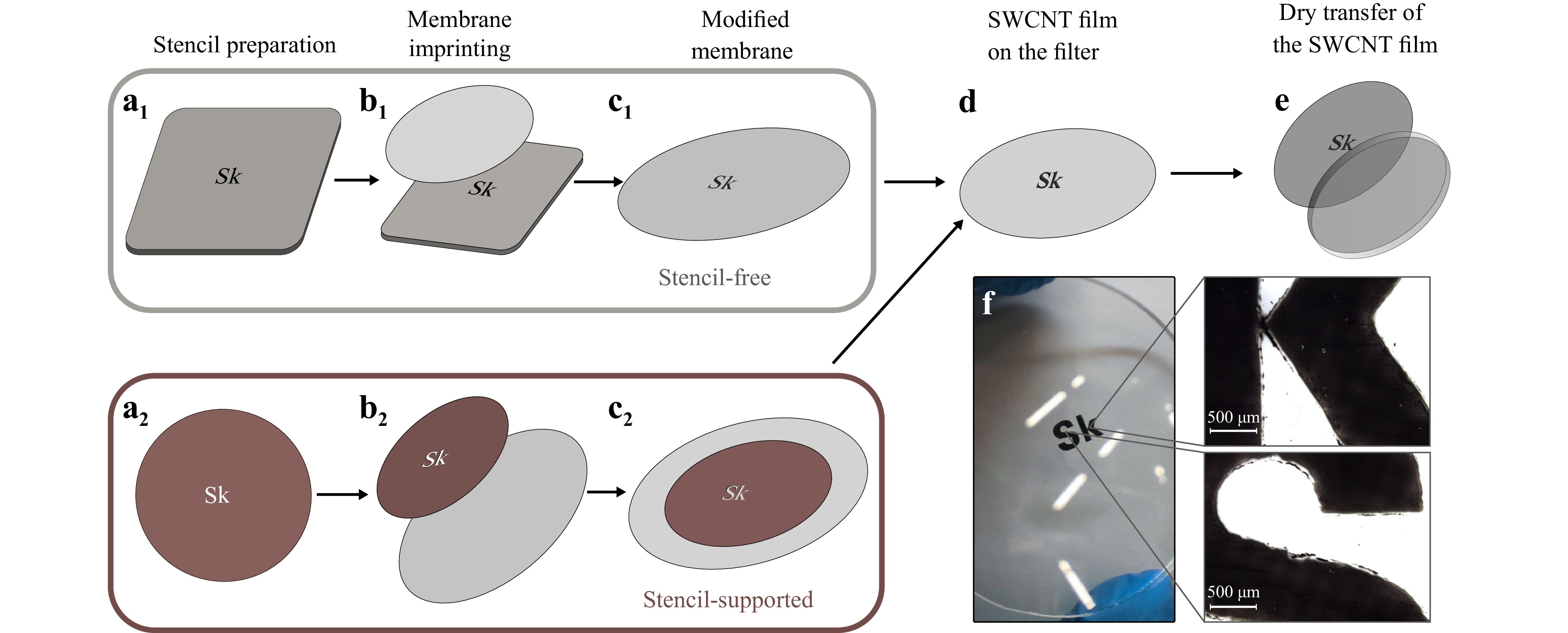
Fig. 1 Schematic presentation of the proposed approach embodied in two patterning modes: Stencil-free variant: a1 A stainless steel plate is engraved with a pattern by laser ablation. Engraving is repeated several times to deepen the pattern for more than 200 µm. b1 Imprinting of the membrane with subsequent detachment of the stencil. c1 The imprinted membrane has an initial thickness at the area of the engraved pattern, while the other regions are thinned due to compressed pores. SWCNT collection is performed on the side, which was not in contact with the stencil during imprinting, to ensure a higher quality of edges. Stencil-supported variant: a2 Laser cutting of copper foil with subsequent PVP coating to increase adhesion for imprinting. b2 Imprinting of cellulose filter, stencil is attached. c2 Stencil-supported membrane. Improvement in pattern reproduction quality for this approach is achieved by a combination of stencil and pressed pores for blocking aerosol paths. For SWCNT collection, the membrane is placed with the stencil attached underneath, on the opposite side with respect to the incoming aerosol. d Collected SWCNT film on the filter. e Dry transfer of the collected SWCNT film on the required substrate. f A photo of a patterned SWCNT film, dry transferred to polymer glass with detailed images of elements obtained by optical microscopy (inset).
The other approach (stencil-supported) is to use 50 µm copper foil ASTM B152, and the pattern is cut right through the whole depth of the foil using Argus SFS30 Fiber Laser Scribing Machine operating at 1,064 nm with 150 kHz frequency and power of 60% (Fig. 1a2). In that case, the stencil is coated with an alcohol solution of polyvinyl pyrrolidone to enhance adhesion to cellulose membrane, and, after imprinting, is not detached (Fig. 1b2, c2). Thus, the SWCNT collection aerosol path flows are blocked not only by the membrane clogging but also by the copper stencil itself. Due to combination of stencil with compressed pores, efficiency of this patterning approach is higher and range of pressure for imprinting was shifted to lower values from 7 to 73 MPa, comparing with stencil-free approach. SWCNTs were collected on the side of the membrane, which had not been in contact with the stencil, for both approaches (Fig. 1d). The surface of the side opposite to the stencil can be considered relatively flat, facilitating the transfer even of tenuous SWCNT films (Fig. 1e). Collecting SWCNTs on the imprinted side of the stencil-free membrane shows a lower quality of the pattern edges due to deposition of nanotubes on the slope between the undeformed and pressed regions. Stencil-supported membranes provide possibility to collect SWCNT films on both sides, however side with attached stencil is restricted for dry transfer thin films.
For testing the resolution of the proposed patterning approach, several designs were prepared with minor differences for stencil-free and stencil-supported variants (Fig. S2a, b). Calibration masks were imprinted with different pressure values in a nitrocellulose membrane, and, after SWCNT collection, the patterned films were then dry transferred on a PET substrate for further assessment of resolution. For the electrical application of the patterned films, a design of pairs of square elements with a gap of different widths between each other was prepared (Fig. S2c). Local thinning of metal stencil in the regions containing gaps <200 µm was observed in optical microscope, that can be attributed to proximity to laser beam size and partial ablation of areas near cutting path. Thinned metal of gaps caused uneven pressure applied during imprinting and led to inefficient deformation of pores with weakened patterning effect. To mitigate above mentioned issue. the mask area for imprinting was decreased for more uniform pressure distribution and higher values of force applied to the unit of area to achieve a significant change in pore size. Thus, both patterning modes were investigated in the pressure range of imprinting from 17 to 453 MPa. The dependence of resistance on pressure value was measured for different pairs of squares.
-
Analysis of pattern resolution was conducted using a Leica DM4500 P LED optical microscope with a camera module. Optical microscopy was used to analyze prepared masks to assess a deviation from predetermined dimensions of drawings for resolution and percolation test (Figs. S2, S3, and S4a). Deviation of the element size on the mask and in initial drawings of the pattern is explained by the presence of dross after the laser cutting and by the laser resolution itself, defined by a beam of approximately 70−100 µm size (depending on focus caused by surface roughness). For the resolution dependence on pressure applied during imprinting, the line width and the gap between them were assessed. Each dimension was measured at least five times, then the value was averaged, and the standard deviation was calculated. For image analysis, ImageJ 1.54g software was used.
-
The patterned SWCNT films of the resolution test were additionally investigated for transmittance in undesired areas (i.e., where no nanotube should appear according to the pattern design). Transmittance of the space between the elements of the pattern was analyzed with a two-beam spectrophotometer, Perkin-Elmer Lambda 1050, set at the middle of the visible range, 550 nm wavelength. By dependence of transmittance on imprinting pressure value, the improvement of blocking flow paths was roughly assessed.
-
The presence of a thin layer of nanotubes between elements of the pattern in undesired areas was assessed by measurement of resistance between squares of the percolation test design. For this purpose, a MPI TS150 probe station modified with automatic movement control was used. The electrical characteristics between squares were measured with Keysight B15000A semiconductor device analyzer with a limit of resistance measurement of 100 GΩ. The obtained values were normalized by reference resistance between two squares without any gap. To properly assess the dependence of blocking efficiency on the pressure applied, the real gap sizes for fabricated SWCNT films were analyzed and compared with the nominal value, initially predetermined in drawing (Fig. S5b, Table S1).
-
Analysis of the patterned SWCNT thin film morphology and edge quality was carried out using a Quattro S (Thermo Fisher Scientific, the Netherlands) Scanning Electron Microscope (SEM). The acceleration voltage and operating current used were 7 kV and 0.28 nA, respectively, for all samples. The sample with the line pattern was measured at atilt angle of 45° to assess the film density (or thickness) and surface roughness (Fig. S6). The ImageJ program was used for image processing.
-
To display the versatility of the technique for multifunctional applications, mechanical strain sensors were also fabricated using the stated method. The design of the strain sensors was based on traditional metal foil strain gauges used standardly (Fig. S2e)31, and a design from a recent publication was used as a reference8. The pattern was prepared with different dimensions of elements (Fig. S7) to highlight the scalability of the technique, its versatility in geometrical design sizes, and to assess the differences these may cause to sensitivity. To fabricate these sensors, the SWCNTs were collected on a modified membrane film. The pattern was then dry transferred onto a thermoset epoxy substrate. The epoxy used for substrate production was a bisphenol A epoxy produced by Axson Sika (Baar, CH), tradename CR-82 with hardener CH 80-2. The two components of the substrate were independently degassed using a vacuum chamber prior to mixing for 30 minutes, after which they were hand mixed in the recommended volume ratio and vacuum degassed once again for 5 minutes. The mixture was then poured into silicon molds conforming to ASTM 638 and allowed to cure at room temperature for 24 hours. For tensile strain sensing, the substrates were mechanically loaded in a uniaxial tensile regime with a crosshead speed of 2 mm/min (corresponding to ASTM 638). Electrical measurements were simultaneously carried out using a Keysight 34410 A digital multimeter. Strain was measured using a physical extensometer, the readings from which were correlated to electrical resistance change to determine gauge factor (sensitivity factor).
-
For the application of the patterning method in THz optics, a spiral zone plate32 was designed (Fig. S2d), fabricated, and examined. Fabricated SZP pattern was transferred on elastomer Elastosil® FILM 2030 250/100 100 µm thickness. Experimental verification of the manufactured optical element was performed using a home-made THz radiation visualization system29,33. A backward-wave oscillator34 with a radiation frequency of 327 GHz was used as a radiation source. A Golay cell mounted on movable platforms was used as a detector. Pixel-by-pixel scanning of the THz field behind the sample was performed with a step of 0.25 mm at the focus of the studied four-charge SZP. The sample was reliably fixed in an electronically controlled iris (Fig. S8) of a stretching device, allowing the sample to be stretched without changing its position relative to other components of the setup. The experimental results were supported by numerical simulations performed with a custom MATLAB code implementing the angular spectrum of plane waves method. Details on the model parameters are provided in Supplementary Materials, Section 2. OAM characterization was performed according to the following procedure29.
-
The proposed solution for patterning SWCNT films is addressed to aerosol CVD synthesis of carbon nanotubes. This synthesis approach implies deposition of carbon nanotubes on porous membranes through the filtration of aerosol. This particular method of nanotube deposition is limited to the usage of only thin porous membranes for further transfer of CNT films to any demanded substrate. Thus, our approach is targeting the modification of membranes to collect a CNT film of predetermined geometry without the necessity for additional processing steps. Direct deposition of carbon nanotubes on a particular material after synthesis without an intermediate substrate can be realized by electrophoresis or thermophoresis; in both cases, deposition on a polymer substrate seems unachievable. Nevertheless, the membrane approach allows further dry transfer from the porous membrane onto almost any substrate, including elastic ones. Thus, the approach, indeed, allows obtaining stretchable SWCNT films on elastic substrates, opening the way for direct writing of the electrode schemes in a single step.
Initially, we assessed two types of membranes suitable for the dry transfer of SWCNT films: Merck Millipore HAWP (mixed nitrocellulose esters, 0.45 µm pore size, 79% porosity) and Merck Millipore GVWP (Polyvinylidene fluoride, 0.22 µm pore size, 70% porosity). Polyvinylidene Fluoride-based filters (GVWP by Merk Millipore) are also applicable for the dry transfer, because of their molecular structure and mechanical properties; this type of filter was not suitable for a substrate-free patterning approach and was excluded from further investigation. Nitrocellulose (HAWP) and PVDF (GVWP) respond very differently to pressing because of fundamental differences in their molecular structure, thermal–mechanical properties, and deformation mechanisms. Nitrocellulose is a rigid, highly substituted cellulose derivative. The nitrate groups strongly restrict the rotation of the glucose backbone. The chains are stiff and have limited ability to slide past each other. PVDF (polyvinylidene fluoride) is a semi-crystalline thermoplastic with flexible carbon–carbon backbones. Its chains can reorient, uncoil, and slide under stress. The main issue with GVWP occurred during stencil detachment from the filter by stretching and deforming the filter. Though we have not used other materials, like polycarbonate or nylon as filters, we assume that they will behave similarly to the GVWP filter. Both materials tend to stretch under pressure and are not as rigid as nitrocellulose. Though dry nylon can be suitable, we are not familiar with commercially available filter types with low adhesion to CNTs. And as for the stencil-supported approach, all filter types with low adhesion to CNTs are suitable due to the absence of a stencil detachment step. We also increased the temperature during the imprinting procedure for the GVWP membranes to improve pore pressing efficiency. However, polyvinylidene fluoride, even at room temperature, showed a significant level of membrane deformation during the imprinting, thereby inhibiting the proper reproduction of the stencil pattern. Compared to the GVWP, the HAWP membranes do not have a specific melting point. We observed no positive effect of heating on the imprinting procedure for the nitrocellulose membranes. Moreover, an increased temperature led only to the destruction of the nitrocellulose fibers, causing the membrane to become brittle. Thus, we further use only HAWP nitrocellulose membranes at room temperature.
We start the discussion with a resolution test. For this, we modified a pattern, commonly used for optical systems, the 1951 USAF resolution test chart35, featuring line/space gratings elements. We also employed the standard elements for photolithography quality assessment, like star pattern (Siemens Star), contact hole arrays, and general scalebar (Fig. 2a). Thus, the pattern consists of an ensemble of various objects to check the peculiarities of the final SWCNT films.
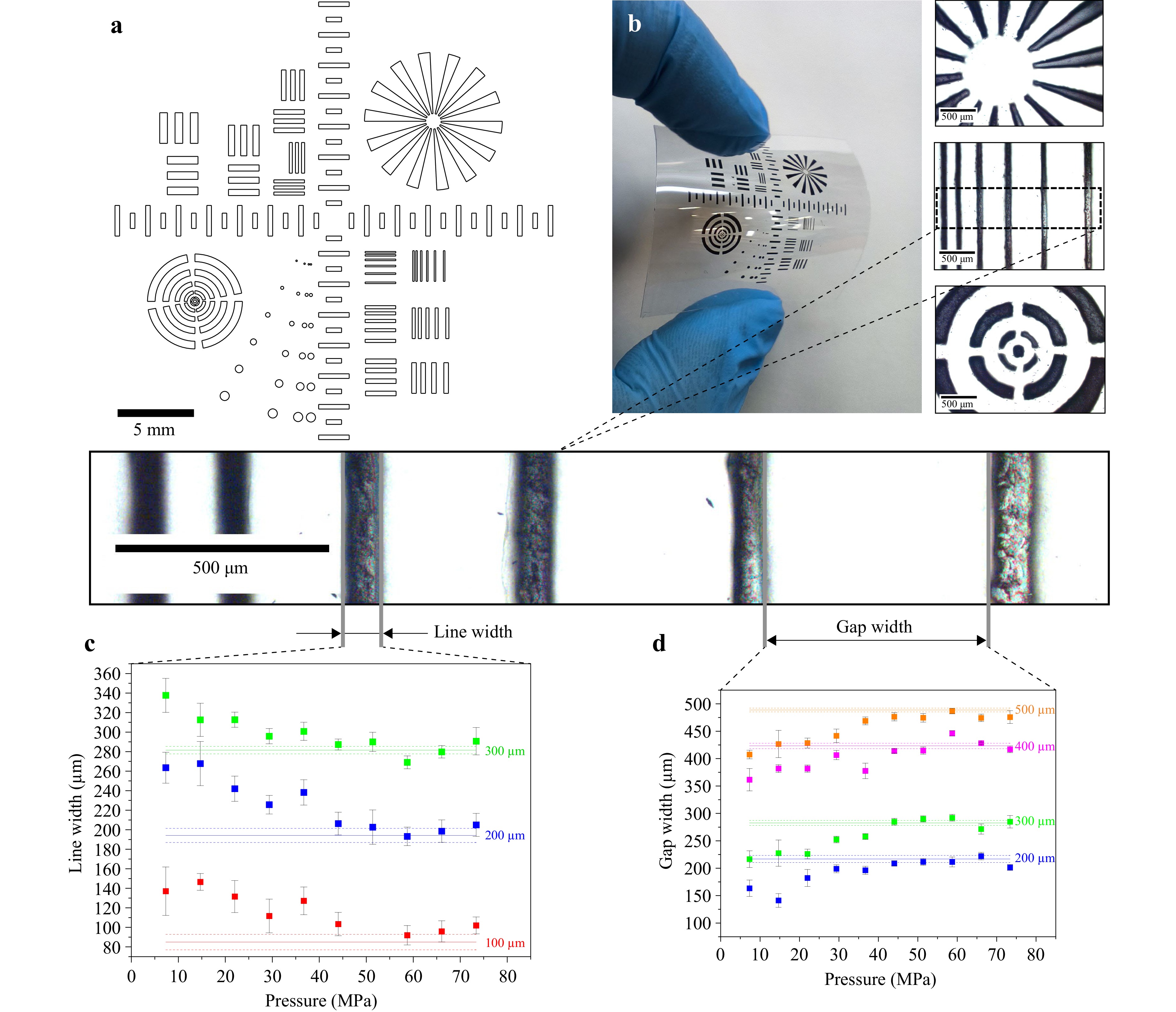
Fig. 2 The resolution test for the SWCNT film deposited on the stencil-supported membrane. a The stencil design for cutting out a copper foil. b Fabricated, using 73 MPa imprinting pressure, SWCNT film of resolution test pattern transferred on PET substrate, inserts: elements of pattern observed with optical microscopy, high resolution, and visual absence of nanotubes between elements were achieved. c Dependence of line width on imprinting pressure applied, continuous lines define the line width measured on the stencil. At pressure higher than 50 MPa, high-level reproduction of initial stencil dimensions was achieved. d Dependence of gap size between line elements on pressure applied during imprinting.
First, the stencil-supported approach was tested, as it helps to benchmarks the minimal pressures needed for the general stencil-free approach. Here, all the pattern elements are isolated to prevent a possible shift due to a poor connection to the entire stencil frame, as well as due to limitations in stencil preparation (as all the elements of the inverse pattern should be connected for this method). Fig. 2b illustrates the SWCNT film (transferred on a polyethylene terephthalate (PET)) with a corresponding pattern (Fig. S9). We qualitatively observe a full transfer of the original pattern to the shape of the SWCNT film. To quantitatively assess the pattern transfer, we analyze the width of thin lines (Fig. 2c; 100, 200, and 300 μm) and the distance between them (Fig. 2d; 200, 300, 400, and 500 μm). We observe the reproduction of the stencil pattern dimensions at pressures higher than 50 MPa. High pressure values can lead to deformation of the stencil itself that may become an issue for good reproducibility of the initially designed pattern. Interestingly, we register no difference in the pressure dependence for different line widths and gap distances. Also, investigation of the space between elements shows almost 100% transmittance with minor deviations defined by the spectrometer resolution, even for the lowest imprinting pressure value applied (Fig. S10).
The optimal pressure of imprinting for a high-resolution pattern is relatively low owing to the combined effect of both the patterned membrane and the stencil supporting it. Indeed, the observed widths of lines are defined by leakages at the edges of the patterned membrane. During the SWCNT collection, a pressure drop induced by the filter leads to partial and reversible membrane deformation. In that case, the highest tension is applied to the edges of the pattern on the mask, increasing the effect of blocking aerosol path flows around the open regions and, in turn, improving the quality of edges in the SWCNT film.
For the stencil-free imprinted membranes, we observe much higher pressures (>150 MPa) required for performance similar to the stencil-supported membranes (Fig. 3). For example, a simple analysis of the transmittance of the SWCNT films, where no nanotubes should appear according to the pattern, shows no nanotube-induced absorbance at pressure values higher than 200 MPa (Fig. 3b). Moreover, the patterned SWCNT films obtained with the stencil-free membranes are characterized by higher roughness of element borders, possibly due to the lower quality of edges on this type of mask, caused by dross from multiple engravings for sufficient depth of pattern, and the presence of an ultrathin film of nanotubes between elements. Also, significant roughness of pattern borders is caused by the necessity for removal of metal from inner element regions of stencil, which is performed by laser movement not parallel to element edges (Fig. S11). Thus, the edges of the pattern were blurred and gradually transitioned to a thin SWCNT film between the lines, complicating the proper formation of the borders. Also, should be mentioned that higher pressure values cause difficulties in detaching the membrane from the stencil without damage because of a higher level of impregnation of the membrane into any roughness of the metal stencil. Thus, higher pressures can indirectly cause issues with pattern quality and its transfer availability. Nevertheless, compared with the stencil-supported mask, the stencil-free approach has no requirement for all elements on stencil to be connected owing to the rigidity of the stencil metal plate. To test the quality of elements, which is impossible to fabricate by cutting through, the star pattern was replaced with meshes (Fig. S11c) of different widths and periods.
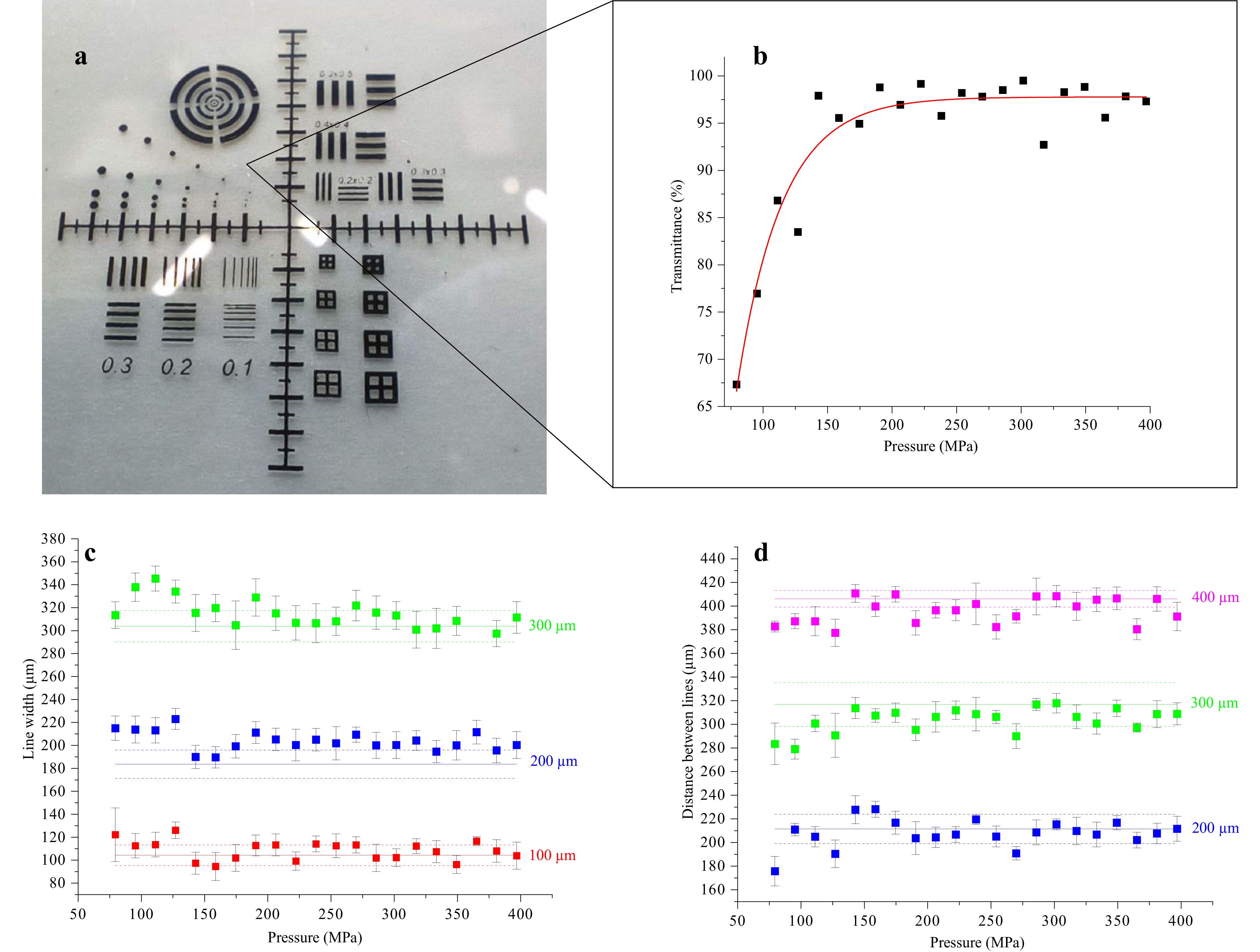
Fig. 3 The resolution test for the SWCNT film deposited on a stencil-free imprinted membrane. a Photo of the patterned SWCNT film on PET. b Transparency at different imprinting pressures for areas undesired for CNT deposition, transparency higher than 95% was achieved at 150 MPa. c Dependence of line width on imprinting pressure applied, continuous lines define the width of the element measured on the stencil. At pressure higher than 200 MPa, high-level reproduction of initial stencil dimensions was achieved. d Dependence of the gap size between the line elements on the pressure applied during imprinting.
To address the possible formation of ultrathin and fully-transparent (i.e., undetectable by an optical spectrometer) SWCNT films between the elements of the pattern, we performed a percolation test for both approaches. The test comprised resistance measurements between two film parts separated by a specific gap with normalization to the reference film without any gap (Fig. 4a). SWCNT films fabricated with the stencil-supported approach performed at 100 MPa imprinting pressure were examined with SEM (Fig. 4). Complete absence of SWCNT film in undesired regions was observed. High quality of element edges without gradual thinning of the SWCNT film at borders was achieved. Also, the film surface shows a uniform distribution of SWCNTs without any traces of patterning effect being transmitted to these regions. For the stencil-free approach, the pressure values of 300 MPa were sufficient to almost completely avoid the percolation between elements with a gap wider than 200 µm (Fig. 4c). At the same time, for the gaps of under 200 µm, sufficient pressure values were higher than 400 MPa, which can be explained by the size of the elements (close to the resolution of the laser used for stencil preparation). The percolation test for SWCNT film collected on a stencil-supported filter showed considerable improvement even for pressures ca. 100 MPa (Fig. 4d). We attribute almost complete absence of percolation to the combined effect of the stencil and the membrane with the clogged pores.
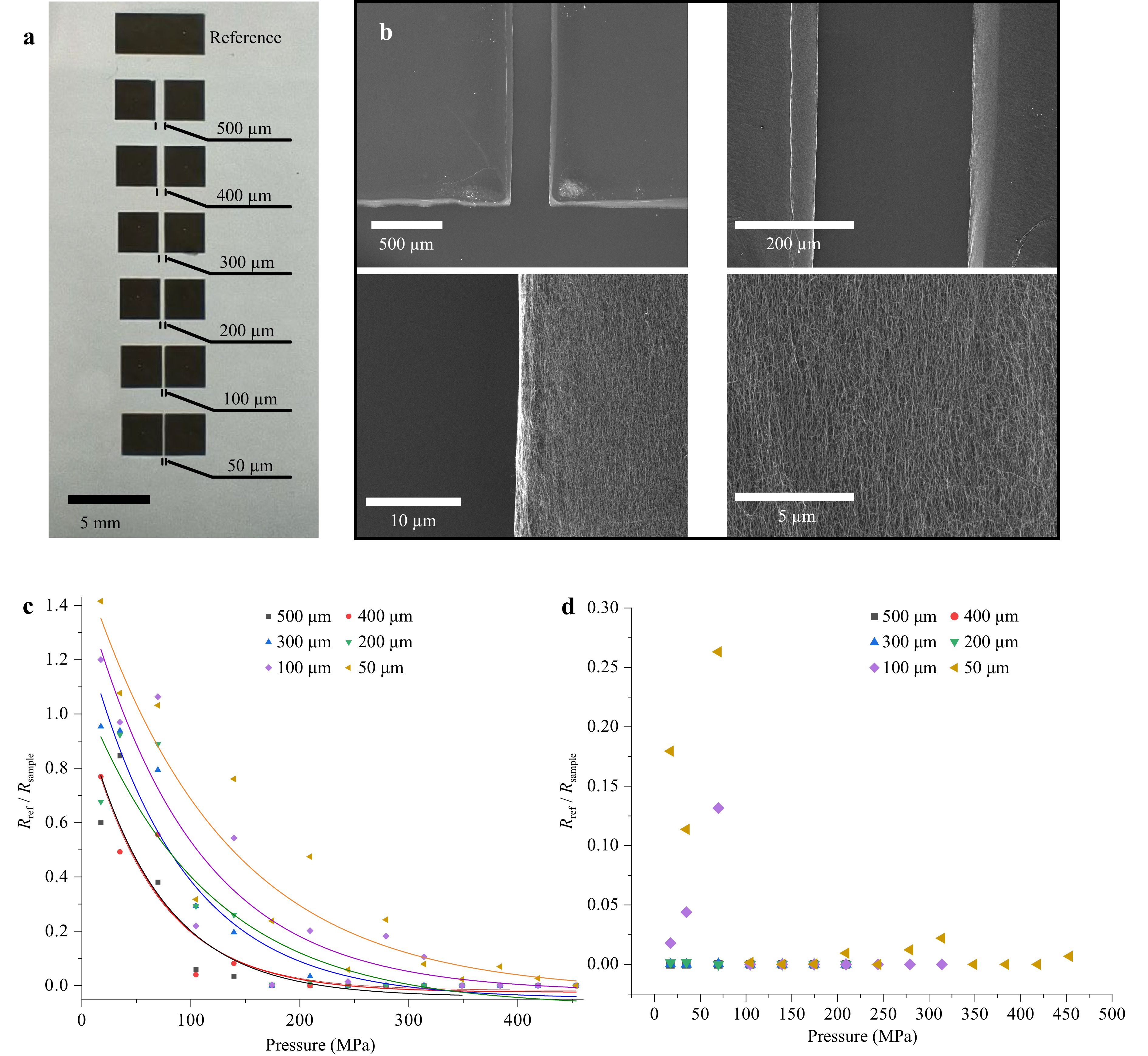
Fig. 4 Percolation test for patterned SWCNT films. a Photo SWCNT film with percolation test pattern on PET. The percolation test pattern consists of pairs of square elements with different sizes of gap between them (50, 100, 200, 300, 400, 500 µm) and a reference without any gap. b SEM images of square element edges and SWCNT film surface for stencil-supported patterning approach performed at 100 MPa imprinting pressure. A complete absence of any nanotubes was registered between elements in undesired areas. Edges of elements are sharp with a steep slope. Image of film surface shows uniform distribution of SWCNTs without any traces of patterning effect being transmitted to these regions. c Percolation test of stencil-free approach patterning fabricated at different imprinting pressures. d Percolation test of stencil-supported approach patterning fabricated at different imprinting pressures. The graphs show resistance between square elements with a different gap size normalized by the reference resistance value.
Our approach was focused on high resolution patterning technique with accurate understanding of influence of such parameters like pressure value of imprinting. Thus, this technique was restricted to small area patterns due to limitations of press equipment maximum force (300 kN). Stencil-supported approach requires less pressure comparing with stencil-free method, however quality requirement for stencil and press plates become much higher. Our assumption was that for large scale membrane modification rollers with pressure adjustment are more suitable than press, but due to access only to simple manual rollers it was decided to conduct all experiments on pressure tunable press. For showing future potential of developed patterning technique to be implemented for large scale CNT films, simple stencil of 8 × 10 cm2 (compatible with manual rollers) was fabricated. After imprinting CNT film was deposited and 13 squares from different regions of membrane (Fig. S12) were dry-transferred for uniformity assessment using optical spectroscopy. For reference 10 × 10 cm2 uniform film was collected and was divided onto 13 regions roughly coincided with patterned CNT film. Absorbance of 13 regions of uniform film was measured and standard deviation was compared with patterned film absorbance. Absorbance deviation of patterned CNT film is 6.2% which is slightly higher than for reference of uniform film 4.0% and is explained by not optimized geometry of scaled filter holder where flow configuration is not consistent. Though after optimization of all components of synthesis and membrane modification we expect high compatibility of developed technique for large scale production of patterned CNT films.
Developed patterning approach allows one to deposit CNT films with a predetermined geometry directly after the synthesis without any extra material or stencil attached to the filter. The previously reported (in situ) methods with extra material being deposited on the filter change the flow distribution of aerosol only in the vicinity of the surface, leading to a significant drop in the film resolution if collection is performed on the side opposite to the clogged surface. At the same time, the high-resolution deposition on the clogged side results in limited film transfer.
Another limitation of the previously reported methods is the requirement to use a specific filter with a particular density of pores for efficient clogging. In the case of the stencil-supported technique, there is no limitation that restricts total throughput during the collection process. For the stencil-free approach, despite being incompatible with the filters showing elastic deformation, no limitations for pore density are observed.
All the post-growth (ex situ) patterning methods usually come with excessive losses of CNTs (which is not the cheapest material in a device as a rule). Such methods as CNC milling or laser ablation of CNT film to form a pattern are characterized by a low-quality edge profile, the presence of individual nanotubes/bundles and carbon residuals in undesired areas8,36. The most proficient in terms of the pattern quality and resolution ex situ method (lithography) is complicated, requires expensive equipment, and has a multistep nature. Different chemicals used during lithography/etching steps, as a rule, contaminate/functionalize the CNTs, diminishing further performance in advanced applications. Also, not all the substrates are compatible with the lithography process as well, while, in the present work, the robust method of the dry-transfer is suitable for most of the substrates.
Our proposed patterning technique is suitable for various advanced applications with strict requirements for resolution and purity of CNT films. The current patterning approach is based on filter imprinting with a metal stencil made using laser ablation. Laser ablation is an affordable and simple method with a resolution limit of approximately 100 μm defined by the beam size, though burning, as a rule, a significant fraction of nanotubes if applied directly to CNT film patterning during post-growth processing. Our patterning approach shows a high reproducibility of stencil geometry with resolution coincident with the laser engraving system. Thus, the resolution achieved is similar to or higher than most of the previously reported methods, excluding approaches with lithography involved. Isolated or poorly connected elements of inverse pattern (grid pattern for transparent electrode, spiral zone plate) become challenging for most of the in-situ patterning methods due to difficulties encountered during stencil fabrication. The necessity of a through cut in the stencil causes displacement issues of pattern elements with low or complete absence of connection to the rigid frame. Stencil-free method allows one to fabricate any desired pattern due to the rigidity of the stencil without a through cut. Regarding filter type suitable for our approach, only the stencil-free case possesses a preference for materials without a tendency for elastic deformations. The stencil-supported approach is applicable for any type of filter due to the absence of a detachment step. All requirements and limitations of the current stage of this new patterning approach are listed in a scheme, which helps to adjust parameters of imprinting for a particular application Fig. 5.
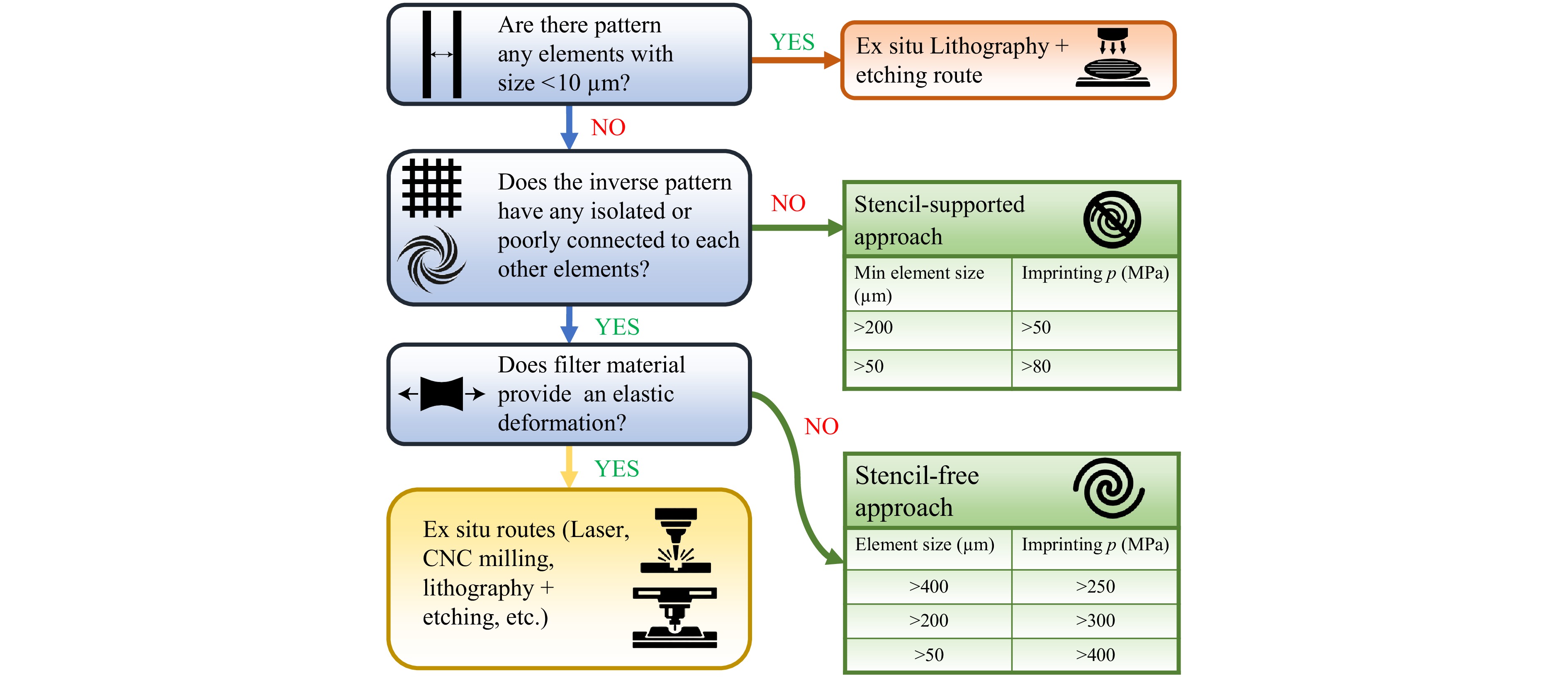
Fig. 5 Block-scheme for choosing the patterning strategy for SWCNT thin films.
We have tested modified membranes in long-term use to assess reproducibility of patterns and stability of quality. Synthesis parameters, collection time and flow were fixed for all samples. Modified membrane with strain sensor patterns was used for SWCNT deposition ten times with dry transfer after each. Collected samples were investigated with optical microscopy and optical spectroscopy. Absorbance measured at 550 nm shows high reproducibility in the range of 3% for different samples. At the same time images obtained using optical microscopy proves preservation of initial geometrical features of patterns after long term usage of modified membrane.
Both patterning approaches were dedicated to be used in combination with laser cutting or engraving for stencil fabrication. Our goal was to introduce a simple method for CNT film patterning using rather cheap and affordable equipment, like laser cutters. In our study, one of the goals was to define the limit of resolution possible to achieve using the proposed CNT patterning method and assess the dependence of pattern quality on the pressure applied during the imprinting of the membrane. For stencil-free and stencil-supported approaches, imprinting pressures higher than 200 MPa and 50 MPa, respectively, CNT films showed high reproducibility of the pattern’s dimensions, which coincides with the stencil. The minimum size of the pattern of the two patterning methods is limited by the resolution of the laser cutting equipment for stencil preparation. In our case, we were restricted by the size of the laser beam, which was approximately 100 μm (depending on focus quality). For small-area patterns, this can be achieved by fine-tuning the laser focus to improve engraving resolution. However, for large area exposure due to surface roughness, the average 100 μm laser beam size limits overall resolution.
Nevertheless, we assume that overall resolution can be significantly improved to tens of microns by a stencil fabrication via optical lithography with subsequent etching of exposed areas to form a deepening of predetermined geometry for membrane imprinting.
As the question of pattern quality directly relates to the edge quality, we assess it with various methods throughout the text:
• the resolution test based on optical microscopy (i.e., pattern size and a gap width in the design versus experimental values (Fig. 2c, d and Fig. 3c, d; quantitative);
• optical transparency of the regions without intentional nanotube coverage (Fig. 3b; quantitative);
• SEM analysis of the edges (Fig. 4b; Fig. S5; qualitative);
• the percolation test (Fig. 4c, d; quantitative).
Though being the most illustrative, the SEM analysis is the only qualitative method here. We agree that the parametrization via “edge roughness or transition width extracted from optical/SEM line profiles” is achievable. Nevertheless, SEM and optical microscopy are limited in sensitivity with respect to electrical studies. Indeed, optical microscopy fails and SEM struggles to observe individual single-walled carbon nanotubes or their small bundles. On the contrary, those could still be easily detected electrically at the lowest levels above the percolation threshold (approximately 7-10 nanotubes per µm2)37. The comparison of optical (Fig. 3b) and electrical (Fig. 4c) data supports the statement. Thus, we believe the percolation test to be the most suitable descriptor. However, apart from optics and sensorics described in the paper, the patterned nanotube films are suitable for various applications (transparent conductors, bioelectrodes, thermoelectrics, heating grids, etc.). This is why we present all the other assessment methods, as they might be more suitable during a specific fabrication stage.
To further highlight the broad applicability of the produced thin films, we employ two prominent applications of the patterned structures: THz optical elements38–40 and strain sensors. We employ the stencil-supported variant for strain sensors (as a single non-interrupted object) and the stencil-free one for the THz devices.
-
SWCNT films are a highly prospective material for next-generation strain gauges because of outstanding mechanical properties, high piezoresistive response, and compatibility with flexible substrates41,42. Demonstrations to date show that the gauge factors of SWCNT films can be much higher than metal foil gauges (but are highly process-dependent)43,44. CNTs have previously been shown to be highly efficient mechanical sensors, not only when dispersed in bulk materials45,46, but also when employed as bucky paper47,48, thin films49,50, or when combined with other structural materials51. Previously, strain sensor designs and scaling were investigated in various studies8,52,53. However, most of the techniques rely on the wet-dispersion of CNTs, which are then patterned through masking or through the physical removal of deposited material to attain the required patterns. These techniques increase the processing steps required both before and after deposition, and are limited in resolution due to the limitations of the abovementioned techniques.
Interestingly, when the fabricated sensors are compared to the best performing design from another study8 (Fig. S7 Reference), the reference specimen in this study (Fig. 6b) displayed a ~10 times greater gauge factor for strain levels until 0.5%, and a ~4 times higher than the maximum achieved gauge factor in the linear deformation range (Table 1). As the reference specimen is scaled down (Fig. 6a), the gauge factor further increases from ~3.0 to ~3.7, highlighting the role of geometry and patterning resolution. Further optimizing the patterning of the films with thinner lines and increased length led to gauge factors of ~4.3 and ~6, respectively, essentially doubling the sensitivity for the last case. It should be noted that although higher calculated gauge factors are possible when the entire deformation range is considered, here, we only calculated for the elastic strain values to ensure reliability.
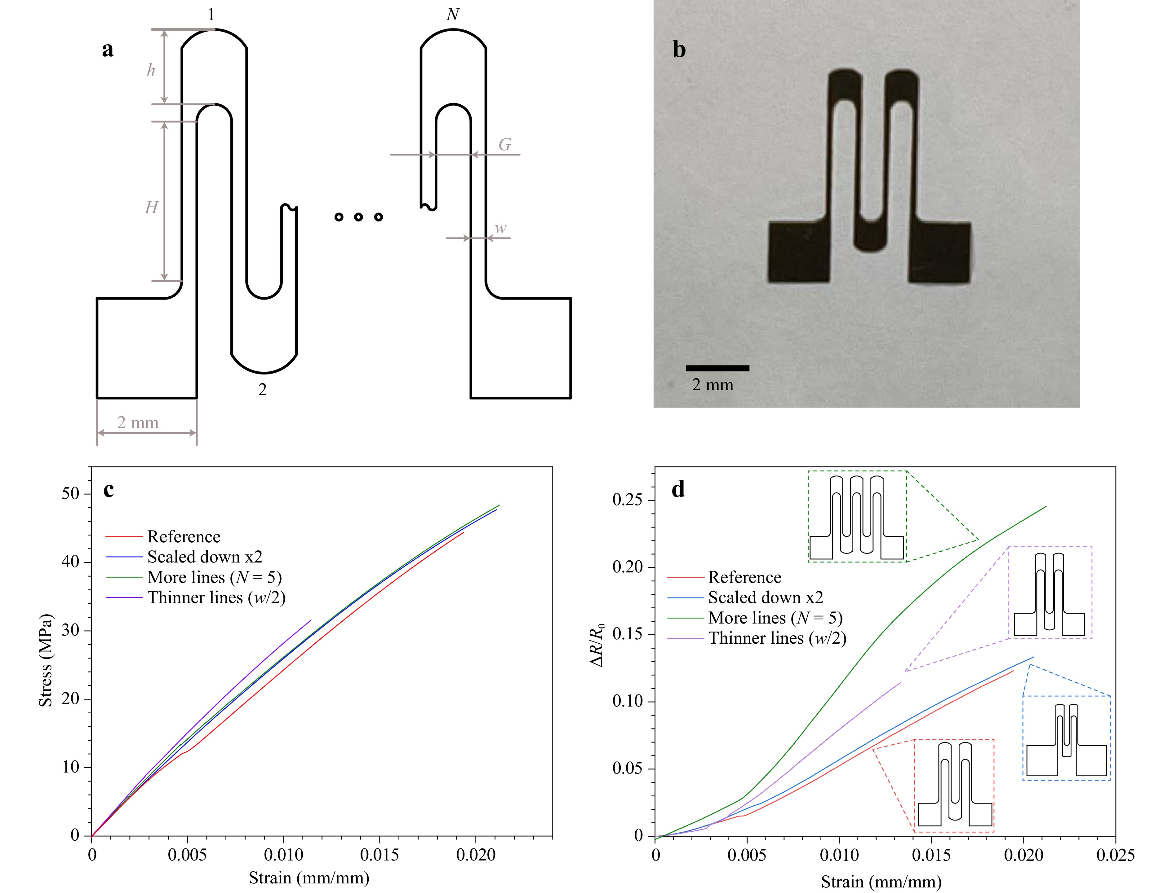
Fig. 6 Strain-sensing test of patterned SWCNT films. a General scheme of patterns used for strain sensor testing, where H is the length of the line, w is the line width, G is the gap width between lines, h is the height of the bridge between lines, and N is the number of loops. b Photo of strain sensor with geometry used as reference. A patterned SWCNT film is dry transferred onto a PET substrate (the PET, in turn, is on a paper sheet). c Dependence of stress in substrate on strain d Piezoresistive response dependence on strain.
Fig. 6d displays the piezoresistive response (∆R/R0) vs. strain of the various patterns investigated, whereas Fig. 6c shows the tensile stress-strain curves of the substrates. Fig. 6a schematically illustrates the various sensors and dimensions. All the parameters of investigated configurations for strain sensing application of patterned SWCNT film are listed in Table 1.
Geometry Name H, mm h, mm G, mm w, mm N GF Reference Reference geometry 3.2 1.5 0.7 0.2 3 0.75 Arana et al.8 Reference geometry 3.2 1.5 0.7 0.2 3 2.7 This work Scaled down x2 1.6 0.75 0.35 0.1 3 2.7 This work More lines (N=5) 3.2 1.5 0.7 0.2 5 5.1 This work Thinner lines (w/2) 3.2 1.5 0.7 0.1 3 2.1 This work Table 1. Parameters of pattern for strain sensor testing (Fig. 6a; H is the length of the line, w is the line width, G is the gap width between lines, h is the height of the bridge between lines, and N is the number of loops). The bold values highlight the difference from the reference geometry; GF is the gauge factor for the elastic deformation regime.
Fig. 6d highlights that the strain gauges follow a relatively linear pattern, where an increase in strain results in a simultaneous increase in piezoresistive response. This behavior changes to a more non-linear response at strain levels of 0.3%−0.5%, which corresponds to the onset of plastic deformation in the substrates (Fig. 6c). The sensors are able to provide strain readings until the fracture of the specimens, indicating that they behave similarly to typical strain gauges.
The piezoresistive sensors designed in this work follow the same principles as conventional metallic foil strain gauges54. Since the patterned SWCNT films are conductors, changes in their physical dimensions (length and cross-sectional area) result in a change in the measured resistance. Considering that the cross-sectional area reduction in caused by the strain the substrate experiences, strain gauges with a longer serpentine length result in a greater value of resistance change, and hence a higher sensitivity55. Thus, by designing the strain sensors with maximum length and optimal cross-sectional areas where the relative change in physical dimensions in maximum, higher gauge factors can be obtained. Further examination and determination of the optimum physical dimensions for the showcased materials is necessary to obtain ultra-high sensitivity strain sensors.
To ensure the reliability of the sensors, the best performing design was subjected to cyclic mechanical characterization for 3,000 cycles, the details of which are included in the Supplementary Section 1 and Figs. S13 (1st-1,000th cycle) and S14 (2,000th -3,000th cycle). To ensure that the strain sensor performs similarly even after 3,000 cycles, the same sensor was used for another round of testing. Here, the stress limit was increased to 8 MPa (border region of the elastic-plastic deformation zone of the substrate), with a strain limitation of 0.003. Strain was measured using digital image correlation (DIC) to determine the gauge factor of the sensors and to identify whether extension drift was taking place. The maximally loaded holding time was also further was increased to 1 minute, whereas all other testing conditions were the same as previously used (supplementary information). The findings are compiled in Fig. 7.
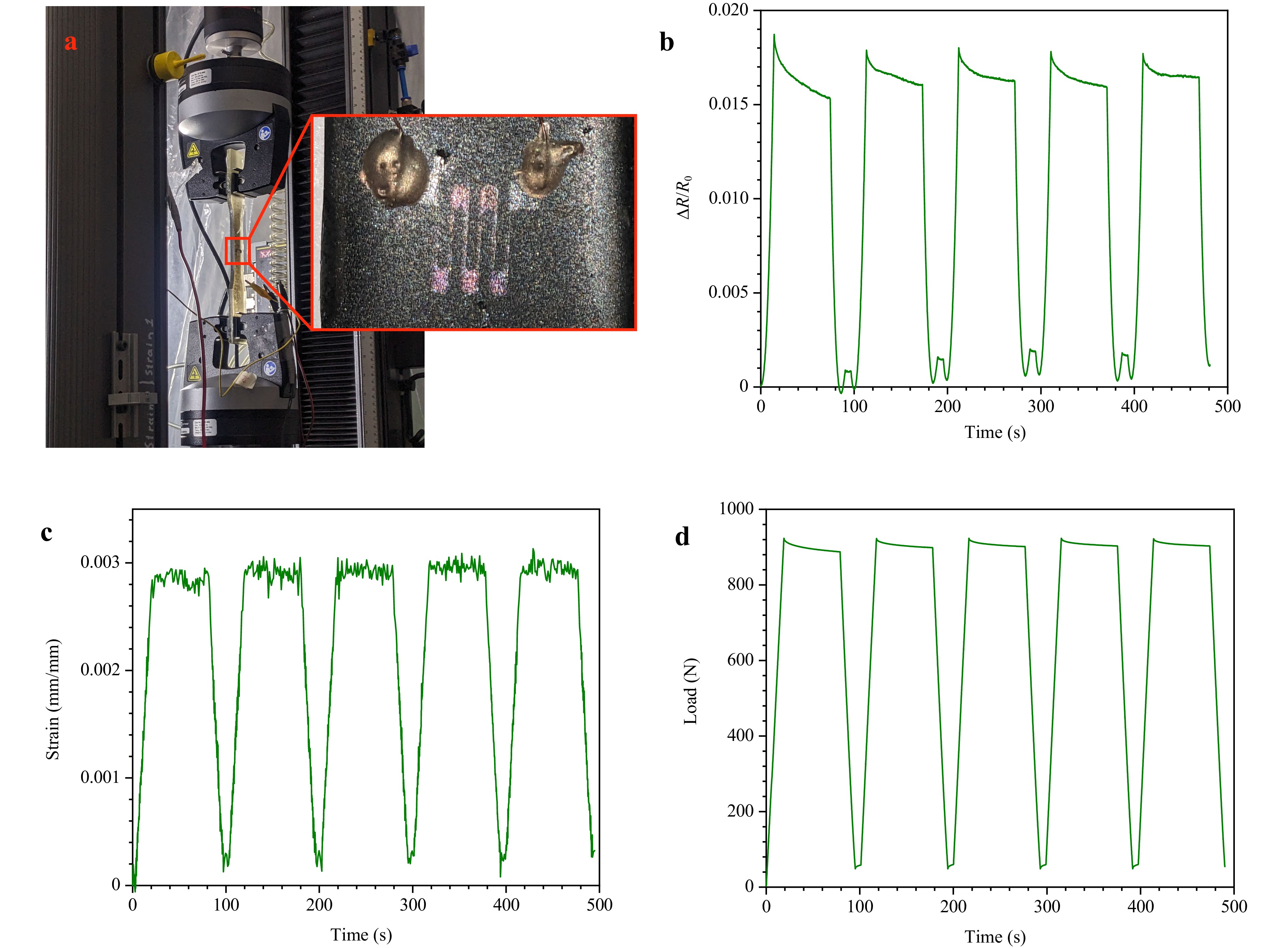
Fig. 7 a A photo of a specimen in the universal testing machine with the inset showing the SWCNT-based strain gauge attached, b The piezoresistive response, and the measured c strain and d load of the substrate.
The characterization after enduring 3,000 cycles confirmed the findings regarding the response and measurement accuracy of the sensor. The piezoresistive response of the sensor indicates the mechanical loading and unloading portions without lag (Fig. 7b), accurately captures the plateaus at the holding times and shows minimum differences between cycles even at higher loading combined with hold time. As shown in Fig. 7c, the DIC strain measurement shows high variance at the maximum mechanically loaded plateau, whereas the load-time graph in (Fig. 7d) depicts a decrease in mechanical loading at the same plateau. This indicates that there is indeed specimen or device-based extension deviation which causes the load to decrease, which is accurately represented by a decrease in piezoresistive response but is not captured by the DIC. This is the same behavior which was noted in the cyclic testing (3,000 cycles), confirming that the accuracy of the sensor is higher than that of commercial techniques. When the strain is used to calculate the gauge factor, values of between ~5−6.6 are obtained, which are in strong correlation with the previous tensile testing conducted (and present in the manuscript). Hence, it is shown that these sensors are highly reliable and can withstand above 3,000 cycles as tensile strain sensors. Furthermore, it is also shown that they display this behavior under both static and dynamic-static conditions, and can be employed with higher sensitivity that commercial techniques such as DIC. The authors believe that further optimization will lead to even greater accuracy and precision, but requires a separate dedicated study.
-
Spiral zone plates (SZPs) represent a highly promising and practical approach for generating and controlling terahertz (THz) vortex beams, functioning effectively as standalone elements56 or within array configurations29. By modulating the intensity, phase, and orbital angular momentum of a THz beam, SZPs enable novel modalities in THz imaging57, communications, and sensing58. To verify the applicability of patterning for designing THz optical elements, we fabricated, modeled, and characterized a four-charge vortex beam generator based on thin SWCNT films patterned as an SZP (Fig. S2d). The evolution of the optical response of the SZP under radial stretching (0% to 12%) is summarized in Fig. 8. It begins with the structural transformations of the SZP itself, shown in Fig. 8a. Fig. 8b then presents the simulated longitudinal intensity distributions, predicting a shift in the focal point. This prediction is tested in Fig. 8c, which directly compares the simulated and experimentally measured 2D intensity distributions at the focal plane, revealing a gradual focal shift with strain that aligns qualitatively with the simulations, despite slight differences in the exact focal lengths. Concurrently, a reduction in the maximum intensity at the focus confirms a degradation of the focusing efficiency upon stretching. This phenomenon is attributed to strain-induced deformation within the SWCNT network, which alters its morphology and reduces its effective thickness, thereby modulating its optoelectronic properties. Furthermore, experimental data reveal a rotation of the intensity pattern with applied strain, an effect not observed in simulations. This discrepancy can be attributed to a slight misalignment between the expected transverse plane and the actual focal plane, on the order of fractions of a millimeter, as supported by the analysis in Supplementary Section 2 (Figs. S16, S17). Additionally, a slight misalignment of the SZP center relative to the optical axis, the impact of which is amplified under mechanical strain, could contribute to this effect.
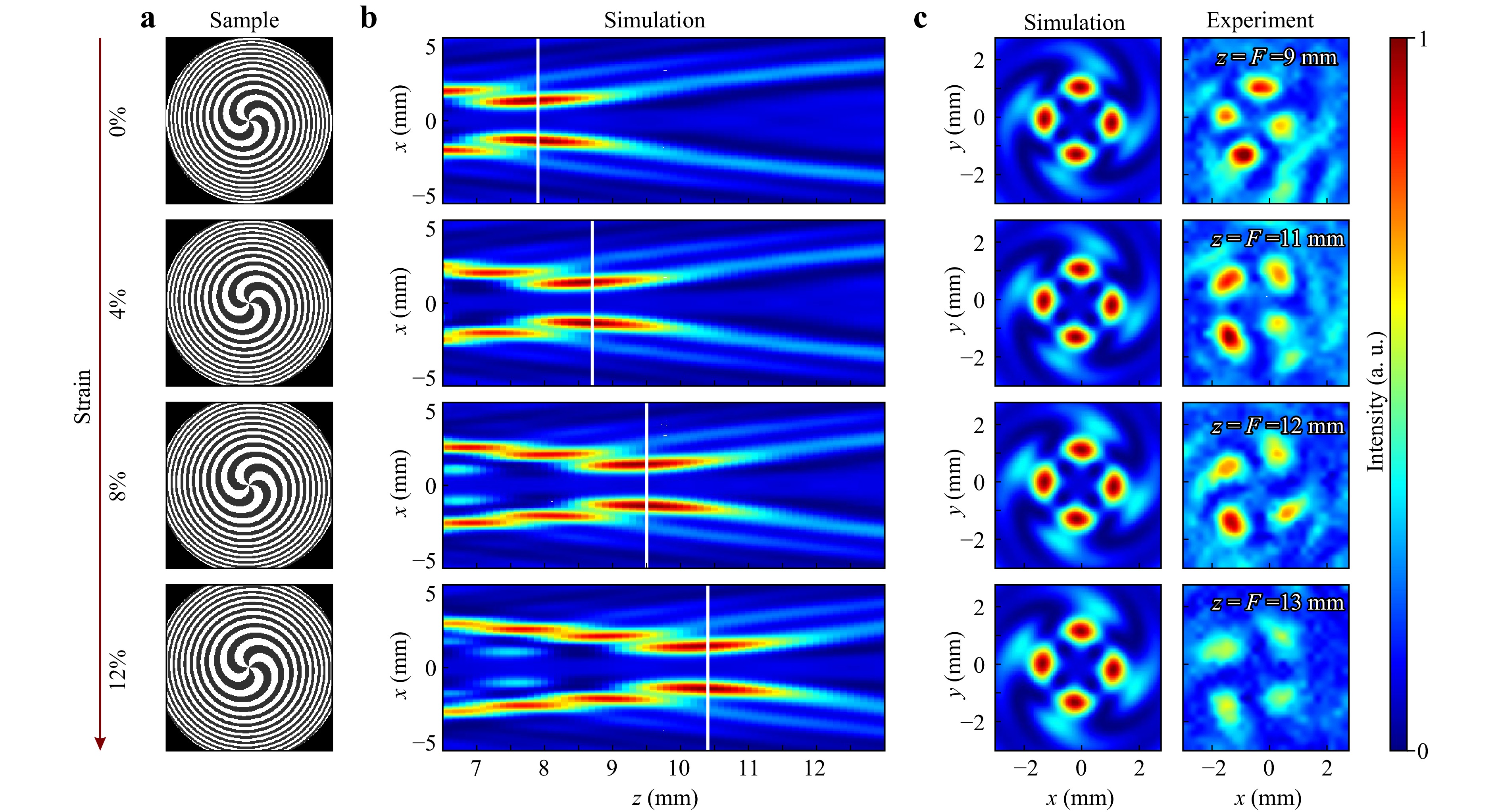
Fig. 8 Performance of a four-charge SZP based on a SWCNT film for focusing a 0.327 THz beam under varying stretching (0% to 12%). a Schematic illustrations of the fabricated SZP structures. b Simulated intensity distribution of the THz electric field in the XZ-plane, where the Z-axis represents the propagation distance from the SZP to the detector. The white lines show the positions of the focal plane corresponding to the stretching. c Comparison between the simulated and experimentally measured THz field intensity profiles at the focal plane.
In the supplementary material, we additionally present, through numerical modeling, THz field phase retrieval using a designed focus-tunable SZP (Fig. S18). This approach makes available the characterization of not only the amplitude distribution but also the phase, providing access to the OAM spectrum (Fig. S19). The principle of multiple-image wavefront retrieval with a focal-tunable device as a scan-free alternative to longitudinal detector translation can be found in the Supplementary Section 3.
It should be noted that the developed technology might be of interest not only for THz but GHz range. The potential applications include novel imaging techniques, telecommunications and the characterization of advanced metamaterials59,60.
-
We developed a novel, robust, and scalable approach for spatially controlled engineering of membranes for the filtration of aerosol SWCNTs. The approach comprises clogging the aerosol filter by applying high pressure on specific places to form a certain pattern. The obtained patterned membranes are reusable, can work in harsh atmospheres, and avoid SWCNT losses. Due to the absence of any post-processing, the obtained films are not exposed to any chemical contamination. Pressure of 200 MPa was shown to achieve a resolution similar to the stencil one (100 µm). Moreover, the performance can be greatly enhanced by keeping the stencil on the membrane after imprinting (P~ 50–100 MPa is needed). A combination of optical spectroscopy, scanning electron microscopy, and electrical measurements proved the absence of any SWCNT in the areas corresponding to the clogged parts of the membranes. The developed active optical device (THz spiral zone plate) enables a shift in focal distance of up to 44% with only a 12% strain. The implemented technology facilitated the development of a fully stretchable THz spiral zone plate and strain sensor, highlighting the further potential applications in optics and electronics. Strain gauge performance in this study displayed a ~10 times greater gauge factor (up to 5) for strain levels until 0.5%, and ~4 times higher than the maximum achieved gauge factor in the linear deformation range, compared with the current advances.
-
This research was funded by the Russian Science Foundation (Project identifier: 22-13-00436-П; SWCNT synthesis, processing, sensor studies). A.V.R and I.E.S. acknowledges the RSF project No. 25–79–30006 (THz studies of nanomaterials). L.L. and H.T. acknowledge the National Natural Science Foundation of China (No. 62475061). The work of AVC, ET and NPV was supported by Ministry of Science and Higher Education of the Russian Federation (project no. FSER- 2025-0007).
High-resolution patterning of reusable membranes for spatially predesigned single-walled carbon nanotube films for advanced optical and sensing applications
- Light: Advanced Manufacturing , Article number: 88 (2026)
- Received: 20 October 2025
- Revised: 27 May 2026
- Accepted: 30 May 2026 Published online: 05 August 2026
doi: https://doi.org/10.37188/lam.2026.088
Abstract: Being one of the most prominent topics, the development of the optically active devices based on lenses and metasurfaces lacks a robust material basis suitable for the terahertz (THz) range. Among candidates such as graphene and dichalcogenides, single-walled carbon nanotube (SWCNT) films offer high modulation depth, durability, and scalability, but precise spatial patterning remains challenging. We present a waste-free, one-step, dry patterning approach that combines aerosol chemical vapor deposition (CVD) with spatially controlled aerosol flow clogging via stencil imprinting. Two approaches are demonstrated. In the stencil-free variant, stencil removal after imprinting yields reproducible features >200 μm and near-complete nanotube suppression in clogged regions at pressures above 200 MPa. In the stencil-supported variant, retaining the stencil enhances flow blocking, achieving complete nanotube exclusion at lower pressures (~100 MPa) and enabling finer features approaching laser resolution. The method is validated through two applications: strain sensors with at least threefold improved response than reported values, and a mechanically tunable THz spiral zone plate with focal shifts up to 44% under 12% strain. This imprinting method offers a scalable route to precisely patterned SWCNT films and opens new opportunities for integrating CNT-based patterns into THz optics and electronic devices.
Research Summary
Carbon nanotube patterning: A waste-free method for precision nanotube films
A new dry, single-step technique lets researchers collect precise patterns of carbon nanotube films directly during synthesis — with no material wasted and no chemical contamination. The method works by physically pressing a metal template into a porous filter membrane, selectively blocking the pores so that nanotubes deposit only where needed. Two variants were developed: one where the template is removed after pressing, and one where it stays in place, enabling cleaner patterns at lower pressures. The team from international consortium demonstrated the technique with two real-world applications: strain sensors outperforming existing designs by up to ten times in sensitivity, and a stretchable terahertz optical lens whose focal point can be shifted by 44% with just 12% stretching — opening new possibilities in flexible electronics and optical devices.
Rights and permissions
Open Access This article is licensed under a Creative Commons Attribution 4.0 International License, which permits use, sharing, adaptation, distribution and reproduction in any medium or format, as long as you give appropriate credit to the original author(s) and the source, provide a link to the Creative Commons license, and indicate if changes were made. The images or other third party material in this article are included in the article′s Creative Commons license, unless indicated otherwise in a credit line to the material. If material is not included in the article′s Creative Commons license and your intended use is not permitted by statutory regulation or exceeds the permitted use, you will need to obtain permission directly from the copyright holder. To view a copy of this license, visit http://creativecommons.org/licenses/by/4.0/.

 DownLoad: