


-
Deep learning has achieved remarkable advancements in recent years 1 , providing effective solutions to various challenges in artificial intelligence, particularly in machine vision applications such as image and video recognition 2 , object detection 3 , and image segmentation 4 . In traditional machine vision architectures, imaging, perception, and processing are considered as separate and sequential tasks because of their distinct functional requirements 5 . Images captured by high-resolution sensors in bulky imaging systems are processed by graphics processing units (GPUs) to expedite computational tasks. However, von Neumann's hardware struggles to meet the computational demands of deep learning models, which presents challenges related to speed, power consumption, and data storage 6 . Recent developments have leveraged free-space optical processing to address these limitations, offering exceptional speed, low power consumption, and the capacity to manage multiple data streams simultaneously 7– 14 . These attributes, coupled with the broad frequency range of light, enable ultra-high bandwidth and data throughput, thereby making optical processors highly suitable for machine vision tasks that demand performance, scalability, and energy efficiency 6, 7, 10, 13- 16 . Optical processors present new opportunities for enhanced functionality and efficiency when integrated with imaging systems. The emergence of all-optical DNNs represents a significant advancement in optical machine vision, employing three-dimensional (3D)-printed diffractive surfaces for image classification and recognition at terahertz frequencies 8, 9, 17, 18 . Early demonstrations of diffractive optical neural networks are often implemented in the terahertz regime, where the long wavelength relaxes fabrication precision requirements and facilitates rapid proof-of-concept validation. However, operation in the visible/near-visible spectrum is more relevant for practical machine vision and camera-integrated platforms. Meanwhile, visible-to-near-infrared (NIR) wavelength implementation demands substantially finer feature sizes and higher neuron densities to achieve wavelength-scale phase modulation and sufficient spatial bandwidth 11, 12, 16, 19, 20 . These requirements impose stringent fabrication precision and scalability challenges for large-area devices. Motivated by these constraints, we developed a high-throughput randomised multi-focus two-photon lithography (TPL) platform that enables the rapid fabrication of high-density diffractive layers at the millimetre scale. Qu et al. demonstrated this potential by developing a high-accuracy optoelectronic hybrid neural network using a single metasurface, which achieved a classification accuracy of 98.05% on MNIST while overcoming misalignment challenges 20 . Recently, Chen et al. introduced LightGen, a dimensionality-manipulation-based all-optical computing framework that enables large-scale photonic integration and optical latent-space transformation 21 , highlighting the emerging role of structured optical dimensionality conversion in scalable photonic information processing. However, challenges introduced by free-space visible-wavelength applications are yet to be addressed, including the need for smaller neuron sizes and higher fabrication precision at large scale, which is constrained by traditional manufacturing methods and design limitations 6, 11, 12, 16 . Existing fabrication techniques such as wet chemical etching and reactive ion etching (RIE) encounter significant obstacles in producing high-density, high-precision diffractive layers necessary for visible-wavelength DNNs 22 . The reliance on costly, time-consuming processes such as electron beam lithography (EBL) limits scalability and practical implementation 22, 23 . In addition, fabrication errors can accumulate across the diffractive layers, restricting the complexity of the model and experimental performance 6, 16, 24 . These issues result in DNNs with limited neuron densities, small model sizes (typically fewer than one million neurons), and suboptimal generalisation capabilities, which makes them inadequate for large-scale machine-learning task 6, 16 .
To address these limitations, random projection-based optoelectronic computing systems have been developed, which are powerful feature-encoding methods that enhance classification performance in machine learning 25– 32 . In our previous work 31 , we experimentally demonstrated that a diffractive neural network based on an optical metasurface composed of 41 million photonic neurons performed random projections. Further, we demonstrated that, at this scale of neuron count, a single-layer diffractive neural network can outperform multi-layered diffractive neural networks and even rival large-scale AI models such as ResNet and Vision Transformers. However, conventional implementations using static scatterers or EBL-fabricated metasurfaces are limited by flexibility, fabrication cost, and environmental constraints.
In this study, we combined this concept with a custom-built randomised multi-focus TPL system 33 , which offers significant advantages in terms of fabrication speed, precision, cost, and structural versatility. This enables rapid prototyping of complex millimetre-scale 3D nano-structures within 15 min without cleanroom requirements, making them highly scalable for large-area optical systems and significantly reducing fabrication time. Finally, we demonstrate a multi-task DNN processor for visible-wavelength image processing using this system. The diffractive encoding device is cost-effectively printed with a density of 4 million neurons/mm 2 and demonstrates significant advancements in neuronal scalability, supporting up to four million neurons. This scalability and high neuron density are enabled by our custom-built randomised multi-focus TPL system, which achieves 500 nm wavelength-scale pixels at a processing speed of 0.267 million neurons per minute. Our processor integrates a diffractive layer with a lens into a compact millimetre-scale design (1 mm) followed by a simple single-layer digital network to process the projected Fourier-region information onto a camera. The proposed system realises superior performance including high recognition accuracy (≥97% accuracy), reduced hardware requirements, and minimal electronic post-processing for various machine vision tasks such as hand-drawn figure classification, object recognition, human action recognition, flow cytometry image classification, and keypoint detection in human faces. The training costs are significantly reduced because only the digital readout layer requires training, thereby eliminating the need for optical network training. Further, our method is compatible with a wide range of imaging systems, enabling the great potential of Optical neural network(ONN)-based devices in applications such as light detection and ranging (LiDAR) 34 , optical coherence tomography 35 , biomedical diagnostics 36 , and human-computer interaction 37 . This integrated approach enhances the scalability, performance, and practicality of DNNs in visible wavelengths, paving the way for their broader application in optical machine vision. Furthermore, this method facilitates cost-effective high-throughput mass production and rapid product development. Overall, this study marks a critical step towards scalable, integrated, and high-performance optical processing solutions that can shift the paradigm in machine vision technology.
-
We present a multi-task optical processor that employs a 3D-printed diffractive optical element (DOE) device with a random phase distribution, as indicated in Fig. 1a. Our ONN image sensor includes an optical linear layer (3D-printed DOE), commercial lens, charge-coupled device (CCD) camera, and digital neural network. This free-space optoelectronic computing system integrates optical processing with a simple digital network using as few as 1,000 parameters. Our device shows exceptional experimental performance, achieving strong classification performance with minimal hardware overhead. Further, we demonstrate the generalisation ability of the processor across various machine vision tasks, as well as its multi-task compatibility enabled by a shared optical front-end that required no retraining for different tasks, as illustrated in Fig. 1.
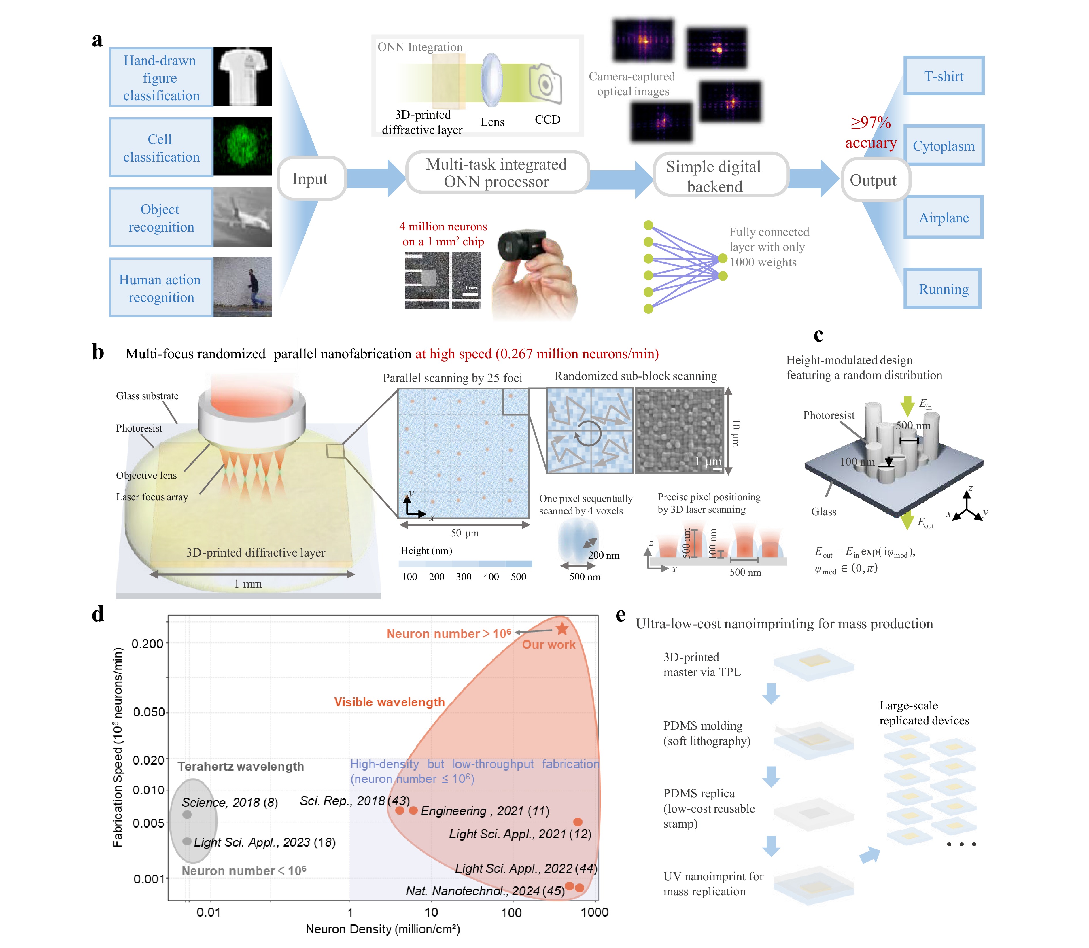
Fig. 1 Multi-task, large-scale integrated optical vision processor using ultra-fast parallel nanofabrication. a Flowchart of the multi-task integrated ONN processor. b Illustration of the randomised multi-focus TPL system printing at a rate of 0.267 million neurons per minute for ONN device fabrication. We propose a random scanning strategy to achieve clearly isolated diffractive pixels with both high spatial resolution and fabrication throughput. In this method, each 10 μm × 10 μm region is patterned with pixels composed of four adjacent voxels arranged in a quadrilateral configuration, spaced 200 nm apart, and exposed simultaneously in a single-shot process. c Comparison with previously reported works including both 3D printing in Ref. 8, 12, 18, photolithography in Ref. 11, 43 and EBL in Ref. 44, 45 (such as neuron number, density, and fabrication speed). d Design of the 3D-printed diffractive layer. Each unit is fabricated from photoresist (n = 1.520 at 520 nm) on a soda-lime glass substrate (n = 1.527 at 520 nm). Five phase gradients with π/5 increments are implemented, facilitated by a height-modulated, untrained design featuring a random and uniform distribution with five distinct levels (heights of 100–500 nm). e Ultra-low-cost nanoimprinting for mass production. The reusable mould is generated by polydimethylsiloxane soft lithography, and large-scale replication is achieved via ultraviolet nanoimprinting with high throughput and high feature fidelity.
In the optical module, a coherent light field encoded with input information sequentially passes through a 3D-printed diffractive layer and focusing lens. The phase modulation of the diffractive layer is defined by an untrained design that employs random height modulation, as indicated in Fig. 1c. Each unit cell was fabricated from a photoresist on a soda-lime glass substrate. The fabricated device has a footprint of 1 mm 2 and comprises laterally stitched square diffractive patterns with a size of 50 × 50 μm 2. Each stitched region implements five phase values via height modulation at five discrete levels (100–500 nm), corresponding to π/5 phase delay increments. The intensity of the transmitted light is detected in the output plane and saved as an image. Subsequently, these intensity images were downsampled to reduce their size for processing using a subsequent digital neural network. The downsampled images were flattened and input into a single-layer neural network, from which the final classification results were generated.
We custom-develop a randomised multi-focus TPL system based on a regenerative femtosecond laser amplifier to fabricate the DOE shown in Fig. 1a ( Fig. 1b). Further, we propose a random scanning strategy that enables the rapid and scalable fabrication of large-area 3D nanostructures by exploiting the 3D random-access scanning capability of the optical engine. To the best of our knowledge, this is the first study to present this strategy. Our method integrates spatiotemporal voxel randomisation with 25-point multi-focus exposure instead of the conventional serial approach while concurrently ensuring pixel-level fidelity and fabrication efficiency (15 min/mm 2). Our prior investigations into pixel density and comparative experiments with an optical diffuser (discussed later) confirm that sub-500 nm pixels are required to achieve high classification performance. Other TPL approaches such as parallel or traditional serial single-focus scanning 38– 42 cannot deliver 3D morphology control at this scale or lack the throughput for high-speed direct writing, whereas our system remains uniquely capable of combining both. In the visible spectrum, previous methods for implementing diffractive layers relied on metasurfaces fabricated via EBL, which required hours and resulted in fewer than one million neurons.
Further, we compared our fabrication approach with other methods commonly employed in ONN development, including 3D printing 8, 12, 18 , photolithography 11, 43 , and EBL 44, 45 . The results are presented in Fig. 1d and Table S1 (see details), which demonstrate that the proposed method offers significant advantages in terms of neuron count, integration density, and processing speed.
As illustrated in Fig. 1e, our approach enables an ultra-low cost and large-scale replication beyond direct TPL. A master device fabricated by high-resolution 3D printing can be transferred into a reusable polydimethylsiloxane (PDMS) mould via soft lithography and subsequently replicated by ultraviolet (UV) nanoimprinting with high throughput and high feature fidelity. Unlike conventional metasurfaces and other optical neural network platforms that rely on one-off or costly fabrication schemes and thus suffer from significant challenges associated with scalability, our method intrinsically supports cost-effective mass production. This unique capability bridges the gap between high-precision prototyping and scalable device manufacturing, thereby offering a practical and economical pathway towards the deployment of optical neural networks.
-
Our previous work has shown that the size and statistical distribution of the projection matrix play a critical role in the performance of diffractive optical computing systems 31 . Traditional methods for implementing such projection matrices often rely on static physical scatterers or metasurfaces fabricated by EBL, which are limited by design flexibility, fabrication cost, and environmental constraints. In contrast, our DOEs are directly fabricated via a multi-focus TPL 33 , which enabled the construction of a large-scale, optically encoded transmission matrix with precisely defined spatial modulation via hundreds of 3D programmable laser foci. Compared to EBL-based metasurfaces, our method offers significant advantages in terms of fabrication speed, cost, and structural versatility. It supports true 3D structuring without requiring vacuum or cleanroom conditions and operates as a single-step direct-write process with no postprocessing requirements. This enables the rapid prototyping of complex DOEs within 15 min, which makes it highly scalable for large-area optical systems.
We implement a randomised multi-focus TPL nanofabrication platform using binary digital micromirror device (DMD) holography (Supplementary Fig. S1) driven by a low-repetition-rate femtosecond laser amplifier (800 nm wavelength, 1 kHz repetition rate, and 100 fs pulse width) to provide high peak power for parallel nanofabrication. The DMD employs a binary-hologram-based weighted Gerchberg-Saxton algorithm for generating a > 99.9 % uniform 3D multi-focus array in the Fourier plane. Subsequently, this array is focused under a dip-in configuration into a droplet of custom photoresist using a 100× oil-immersion objective (NA = 1.3), and the photoresist has a post-polymerisation refractive index of 1.520 at 520 nm 33 .
Unlike conventional TPL systems that print DOE pixels sequentially, our randomised scanning strategy combines temporal randomisation with spatial parallelisation. Within each 50-μm-wide DOE unit, pixels of 500 nm lateral pitch and height levels ranging from 100 to 500 nm are realised, with the z-positions of the laser foci defining the final height, thereby enabling a direct 3D phase gradient structuring. Each pixel comprises four adjacent voxels arranged in a quadrilateral (200 nm spacing); each voxel is exposed to a single femtosecond pulse, and the four voxels are sequentially exposed to four consecutive pulses to prevent capillary-force-induced collapse and ensure structural robustness 33, 46 . Traditional sequential exposure normally causes polymerisation-diffusion-induced pixel merging and blurred boundaries. A temporal interval of at least 20 ms is enforced between neighbouring pixel exposures to suppress this issue. We employ a randomised sub-block scanning scheme across 25 parallel foci to isolate pixel exposures and suppress crosstalk and stitching artefacts, while enabling a fast fabrication time of only 1.6 s per 50 μm unit. The results of both random and sequential scanning methods are shown in Fig. S2 and movie S1. This randomised multi-focus scanning strategy is the first demonstration that combines voxel-level randomisation with parallel multi-beam exposure to ensure high pixel fidelity and rapid production ( Fig. 1b- e). During large-area writing, a piezoelectric hexapod compensates for stitching alignment errors with sub 100-nm precision, thereby enabling the high-quality assembly of microscale thickness structures across millimetre scales and rapid prototyping of complex diffractive optical elements (Supplementary Fig. S6). Accounting fo the stage-stitching time, the entire 1 mm 2 area is fabricated in only 15 min.
-
Random projections through linear optical scattering have proven to be highly effective in signal processing and machine learning, particularly in feature-encoding-based dimensionality reduction tasks 25– 27, 29 . For datasets with many features, the goal is to identify transformations that reduce dimensionality while preserving pairwise distances between data points. The Johnson-Lindenstrauss lemma confirms that linear random projections are well suited for this purpose, offering properties that enhance classification performance 26, 27, 47 . Based on this, we develop a simulation model shown in Fig. 2a. In this model, the random matrix $ W $ controls the phase of the input image from the MNIST and Fashion-MNIST datasets, with a specific phase coverage. Subsequently, the phase-controlled image is subjected to Fourier transform using an optical lens. The output image is then flattened and fed into a single-layer network, from which the classification results are generated.
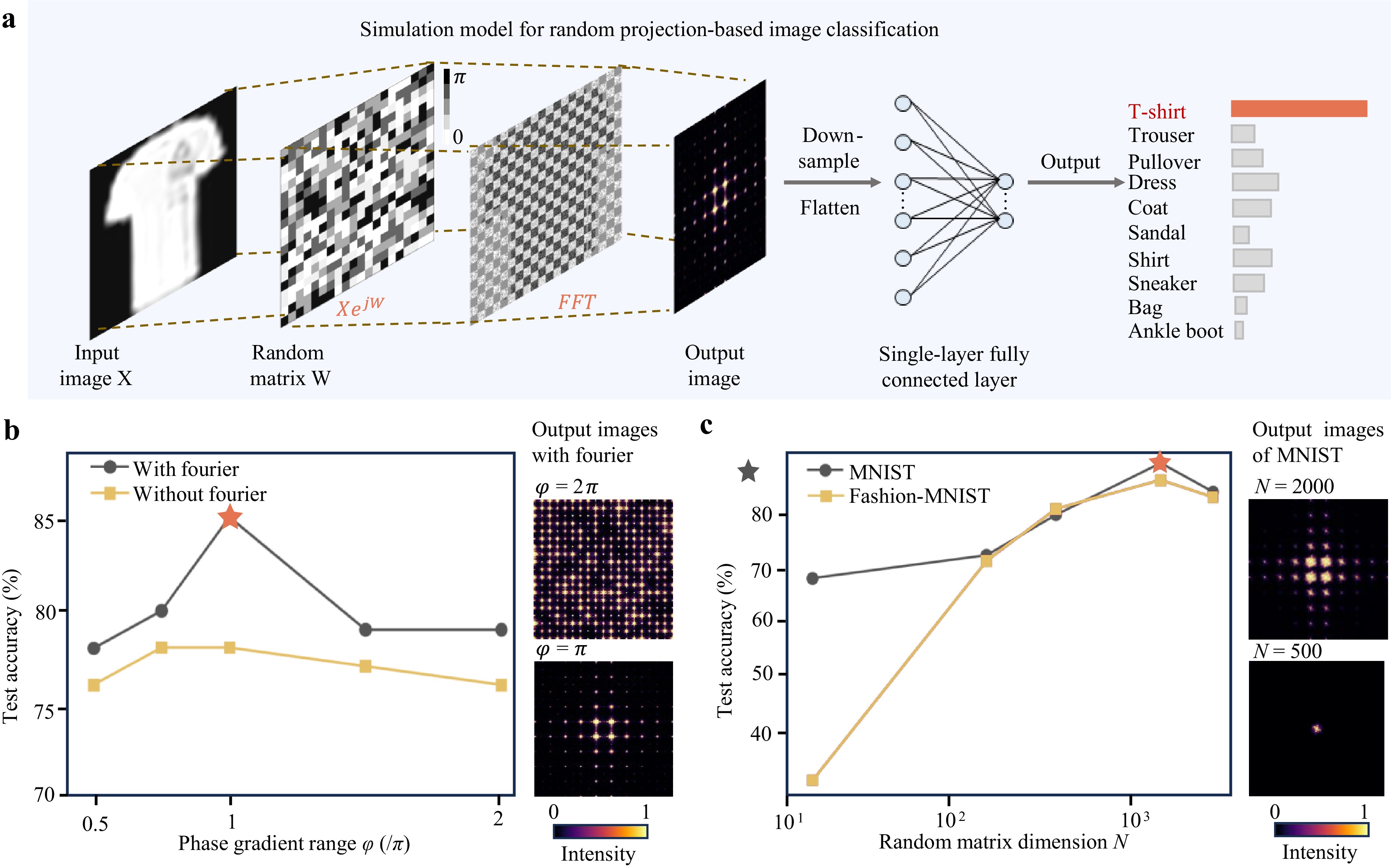
Fig. 2 Simulation results for random projection-based image classification. a Simulation model used for random projection. b Simulated classification accuracy for the Fashion-MNIST dataset across different phase gradient ranges ( $ \varphi $), spanning from π/2 to 2π. The results are compared for two scenarios: with Fourier transformation (dark gray line) and without Fourier transformation (yellow line). The inset images show output images after random matrix and Fourier transformation for different phase coverage ranges. c Simulated classification accuracy for both the MNIST (dark grey line) and Fashion-MNIST (yellow line) datasets, evaluated with varying dimensions of the random matrix in the range of 20–2,000. The inset images illustrate output images from the MNIST dataset after random matrix and Fourier transformation as the random matrix dimension changes.
In our simulations, we evaluate the impact of phase coverage, Fourier transformations, and random matrix dimension on classification accuracy, as shown in Fig. 2b, c. When the phase coverage is set to π and Fourier transformation is applied, the classification accuracy is maximised, reducing the complexity of our design. These simulation results form the basis of our final device design and configuration presented in Fig. 1a, wherein we select a phase coverage range of π and incorporate a commercial lens for Fourier transformations. To realise this modulation, as given by $ \varphi =h\cdot {n}_{\text{eff}}\cdot 2{\text{π}} \slash \lambda $ 48, 49 , we discretise pixel heights from 100 to 500 nm in 100 nm steps, implemented via the randomised multi-focus TPL system. The random matrix dimension is set to 2,000, which corresponds to a printed pixel array of 2,000 × 2,000 pixels, each 500 nm in size. Consequently, we fabricate a 1 × 1 mm 2 pattern. As outlined in a previous work 12 , achieving a neuron density of millions per square meter is critical. We design a diffractive layer with a unit cell period of 500 nm to meet this requirement. The layer dimensions are set to 1 mm, which are consistent with a random matrix of size 2,000 × 2,000. The focal length of the Fourier lens is carefully selected to ensure that the dominant spectral components are adequately sampled (captured by the CCD sensor), while maintaining a compact system footprint.
-
We first conduct several image-classification tasks to evaluate the performance of the ONN processor ( Fig. 3). For benchmarking, the classifiers are trained on ten pre-selected classes from the MNIST and Fashion-MNIST image datasets. The input images, sized at 28 × 28 pixels, are binarised, displayed, and padded on a spatial light modulator (SLM) positioned in front of the image sensor, operating in either a linear single-layer or non-DOE mode. After passing through the ONN processor, the captured data are processed using a single-layer fully connected network (FCN) with 1,000 digital weights to extract classification results. (The same physical DOE sample is employed across all demonstrated tasks. The diffractive layer implements an untrained random projection, and therefore, it serves as a task-agnostic optical encoder, whereas task adaptation is achieved exclusively by retraining the lightweight digital readout layer.)
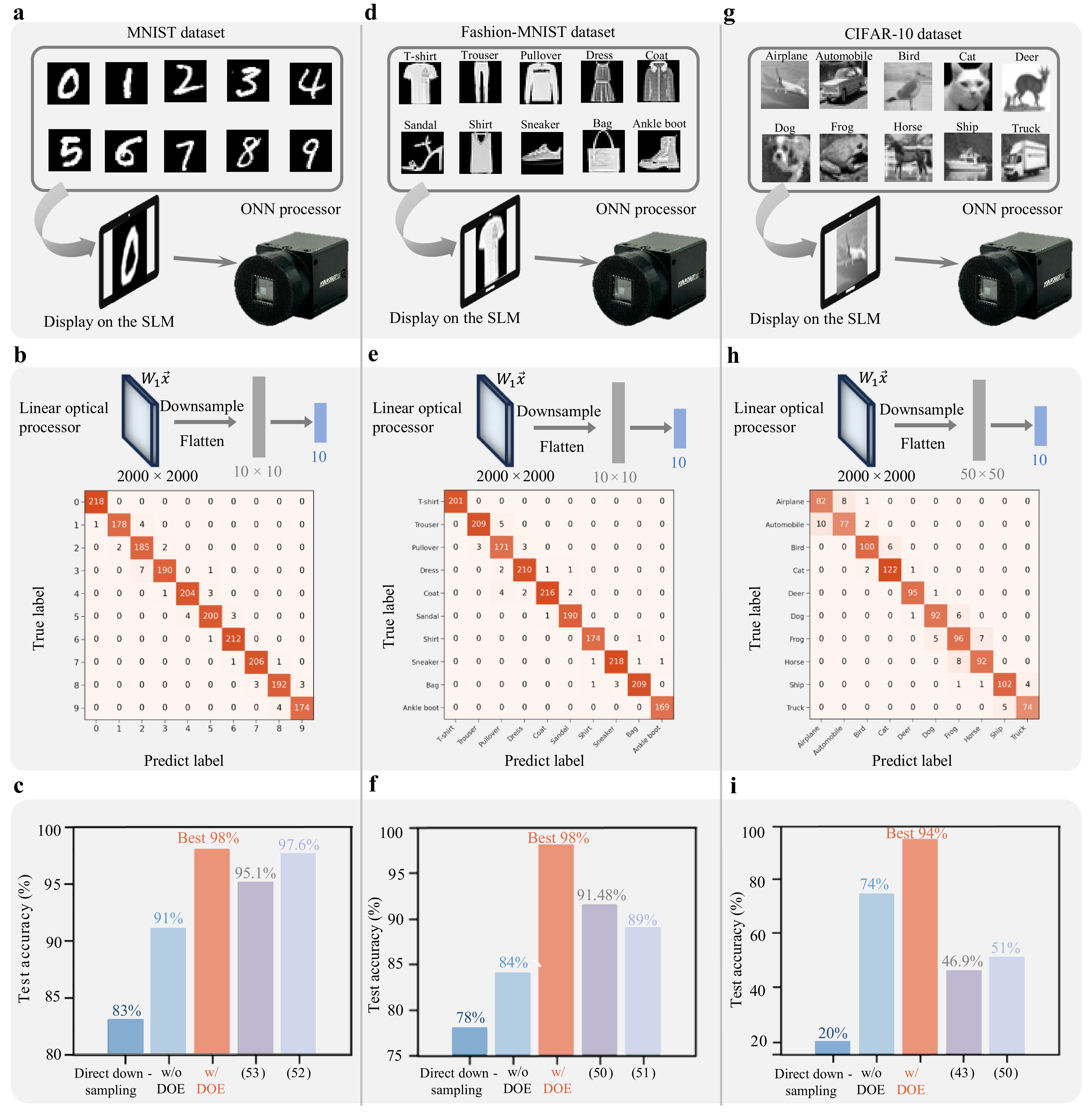
Fig. 3 Performance of the integrated ONN processor in image classification tasks (MNIST, Fashion-MNIST, CIFAR-10). Here, 'w/o' (w/) indicates 'without' (with) DOE mode. a Classification of hand-drawn figures from the MNIST dataset. b Confusion matrices for the MNIST dataset with 1,000 digital weights. c Accuracy comparison of classifiers with different frontends (output dimension: 10 × 10 pixels). The ONN processor achieves 98% accuracy, outperforming processors without DOE mode, direct downsampling, and other free-space ONN processors in Ref. 52, 53. d Classification of hand-drawn figures from the Fashion-MNIST dataset. e Confusion matrices for the Fashion-MNIST dataset with 1,000 digital weights. f Comparison of the accuracy of classifiers featuring different frontends (Output dimension: 10 × 10 pixels) shows that the ONN processor obtains an accuracy of 98%. This performance is superior to those of processors not operating in the DOE mode, and those with direct downsampling, and other free-space ONN processors in Ref. 50, 51. g Classification of figures from the CIFAR-10 dataset. h Confusion matrices for CIFAR-10 with 25,000 digital weights. i Accuracy comparison among classifiers with diverse frontends (output dimension: 50 × 50 pixels) reveals that the ONN processor achieves 94% accuracy. It outperforms processors without DOE mode, direct downsampling processors, and other opto-electronic processors in Ref. 43, 50.
The vector dimension of the digital decoder (FCN) is fixed at a 10 × 10 array to ensure a fair comparison. This corresponds to a 7.84:1 image compression ratio. The large-scale ONN processor demonstrates superior performance, outperforming processors that either operate without the DOE mode or rely on direct image downsampling. Compared to other free-space ONN processors, our system achieves higher classification accuracy, as shown in Fig. 3c, f 50– 53 . Specifically, the MNIST dataset achieves the highest reported accuracy of 98%, whereas the Fashion-MNIST dataset reaches approximately 90% accuracy in existing diffractive optical networks 6, 50– 53 . In contrast, our proposed system achieves 98% accuracy for both datasets.
We further test the optoelectronic computing system using a more complex dataset of CIFAR-10 images. A single-layer FCN with 25,000 digital weights decodes the output of the optical processor. As shown in Fig. 3i, our system achieves an accuracy of 94 %, which is significantly higher than that of the non-DOE mode (74%) and direct downsampling (20%). A comparison with other optoelectronic processors reveals that our system achieves notably higher accuracy ( Fig. 3i) 43, 50 . Furthermore, a double-layer DOE configuration is evaluated for CIFAR-10 image classification (see Supplementary Fig. S8 of the experimental setup). The double-layer DOE design further improves the accuracy to 95%, highlighting the scalability of the proposed system. In addition, a holder is fabricated using fused deposition modeling (FDM) 3D printing technology to secure double-layer DOE samples. The interlayer spacing between the two DOE layers is set to 3 mm, as shown in Supplementary Fig. S8b. The proposed two-layer DOE design exhibits good robustness against propagation distance variations along the z direction, and pixel-level alignment in the x- y plane is not required.
We test our system for action recognition and classification of fluorescent cell organelle images obtained using flow cytometry to explore real-world applications ( Fig. 4). We use the same post-processing neural network shown in Fig. 3 for these tests. For the action recognition task, we select ten categories from the Weizmann Human Action dataset 54, 55 , as illustrated in Fig. 4. Frames that underwent background subtraction are broken down into individual image sequences, binarised, presented on the SLM, and processed using the ONN processor. With an image compression ratio of 75:1, the ONN processor achieves 97% accuracy using only 1,000 digital weights, outperforming both non-DOE (74%) and more complex optoelectronic systems (83% with 4,000 weights 5 ). Compared to directly using complex electronic networks such as ResNet18 56 , our optical processing system achieves a performance (99%) comparable to that with 81,000 digital weights. This reduces the number of digital weights by a factor of 130, clearly highlighting the advantages of optical computing. Fig. 4b, c present confusion matrices for the Weizmann dataset with 1,000 digital weights. These matrices demonstrate the excellent performance of the system, outperforming direct image downsampling.
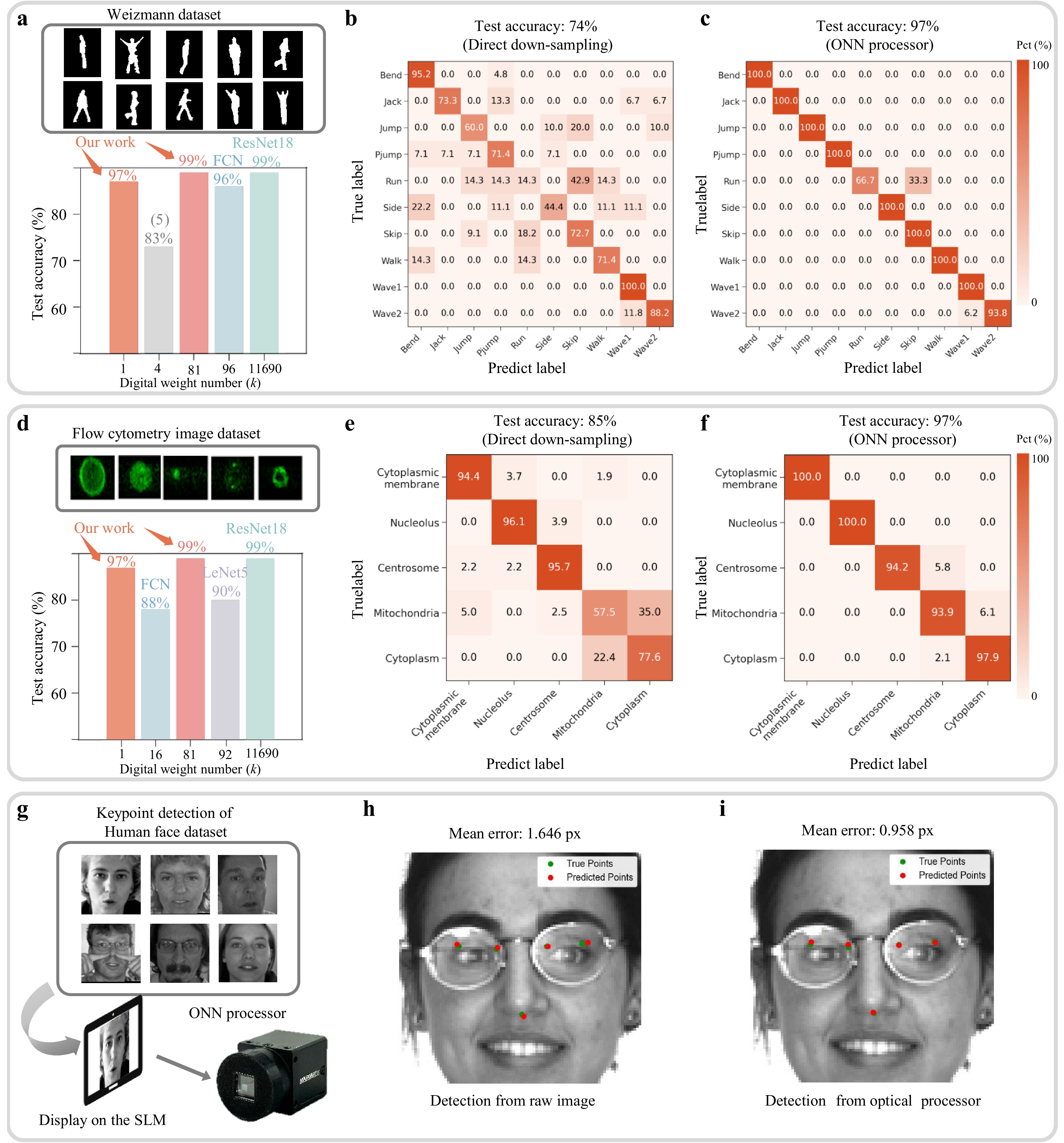
Fig. 4 Performance of the integrated ONN processor in complex vision tasks. a Classification accuracy of the Weizmann dataset with varying digital weight numbers. Our system achieves a classification accuracy of 97% using a single-layer FCN with only 1,000 digital weights, surpassing the 83% accuracy reported by multi-layer nonlinear optoelectronic processors employing 4,000 digital weights in Ref. 5. When optical preprocessing is employed, our system matches the 99% performance of electronic networks other electronic networks like ResNet18 in Ref. 56 while using 130 times fewer parameters, demonstrating the superior efficiency of optical computing. b, c Confusion matrices for the dataset with only 1,000 digital weights. Our system achieves 97% accuracy c, outperforming direct downsampling (74%) b. d Classification of HeLa cells labelled for different organelles from a flow cytometry dataset in Ref. 57 with varying digital weight numbers. Our system achieves 97% accuracy with 1000 digital weights, outperforming a single-layer FCN with 16,000 digital weights and LeNet-5 with 92,000 digital weights in Ref. 58. Similar to the previous case, our system achieves comparable performance (99%) with a 130-fold reduction in digital weights compared to that of electronic networks such as ResNet18 in Ref. 56. e, f Confusion matrices for the datasets with only 1,000 digital weights. Our system achieves 97% accuracy f, outperforming direct downsampling (85%) e. g Keypoint detection on human face images (96 × 96 pixel, as reported in Ref. 59) using the optical processor. h, i The mean error across five keypoints from the optical processor is reduced to 0.958 pixels i, in contrast to the 1.646 pixels from raw image detection h.
Our system exhibits high efficiency in image-based flow cytometry, wherein cells are classified according to fluorescence or phase images. The binarised images of HeLa cells labelled with different organelles from a dataset 57 are displayed on the SLM and classified using the ONN processor. As depicted in Fig. 4d, our ONN processor reaches 97% accuracy with 1,000 digital weights and a 16:1 compression ratio, outperforming a single-layer FCN with 16,000 digital weights and LeNet-5 with 9,000 digital weights. 58 In comparison to directly using complex networks such as ResNet18 56 , our optical preprocessing system achieves comparable performance (99%) with a significantly reduced number of digital weights (130 times fewer). As indicated in Fig. 4f, the confusion matrices for the flow cytometry dataset with 1,000 digital weights demonstrate 97% accuracy, outperforming direct image downsampling (85%) ( Fig. 4e). This performance underscores the potential of ONN systems for high-throughput, low-latency applications such as detecting rare cancerous cells at a rate of 100,000 cells per second 57, 60, 61 .
We further investigate advanced computing tasks such as extracting five keypoints from human face images (96 × 96 pixels from the Kaggle facial keypoint detection dataset 59 ), as shown in Fig. 4g- i. The ONN processor achieves a reduction in the mean squared error by employing the identical digital network architecture for decoding (refer to Supplementary Fig. S7). This decreases from 1.646 px ( Fig. 5h) to 0.958 px in the case of raw image detection ( Fig. 5i). This improvement serves as strong evidence of the robustness of our approach in various applications, including facial recognition, emotion detection, and human-computer interaction systems 37 . In the process of keypoint detection, we harness Python's Dlib library to generate five keypoints. Further, our method provides additional benefits in terms of privacy protection and adversarial robustness 37 . This is because facial information is securely encrypted within random speckle patterns (for more details, see Supplementary Fig. S7).
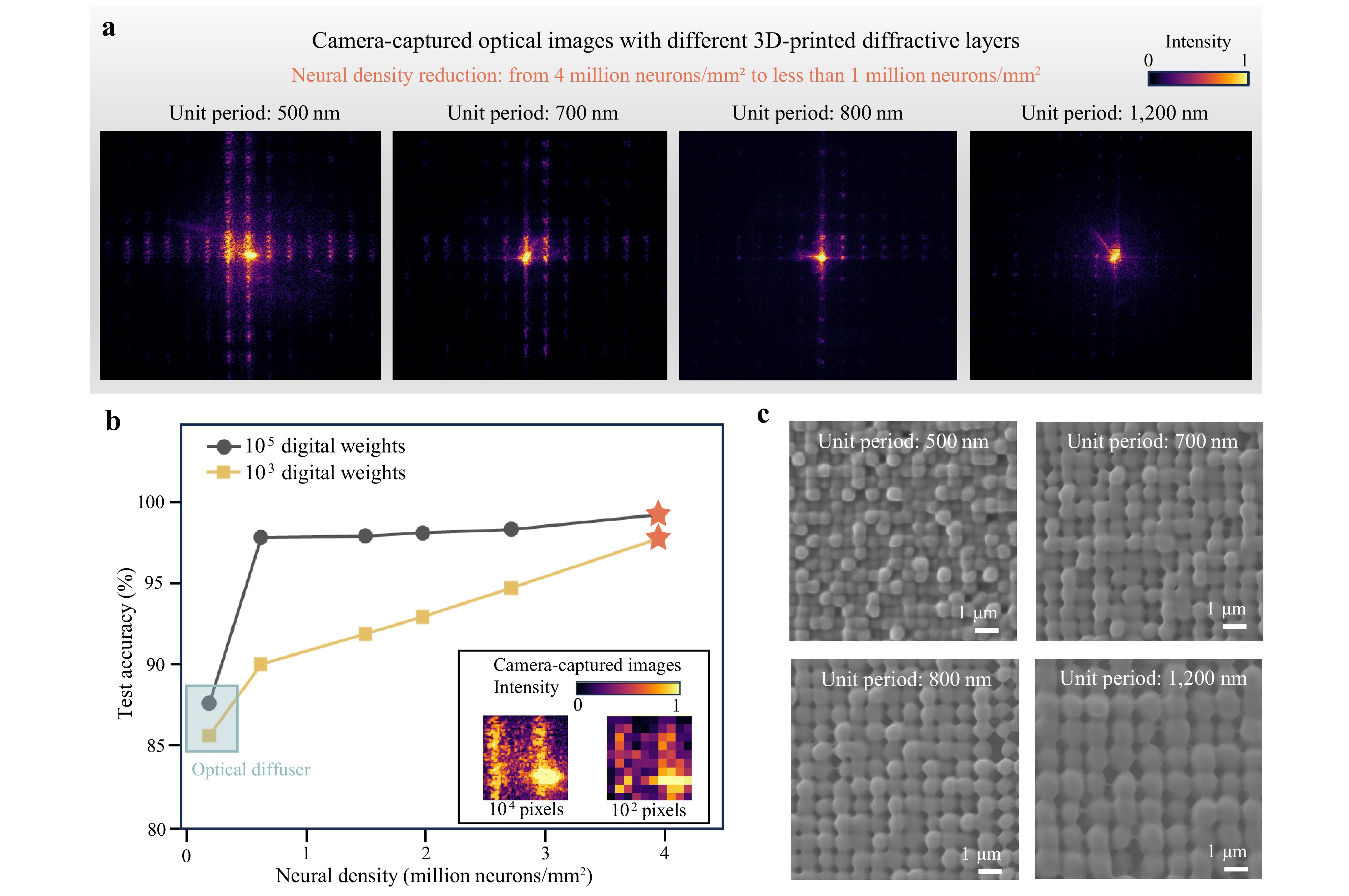
Fig. 5 Effect of neuron density on classification accuracy using the Fashion-MNIST dataset. a Camera-captured optical images of different 3D-printed diffractive layers with unit periods of 500 nm, 700 nm, 800 nm, and 1,200 nm. b Experimental classification accuracy of the ONN image sensors with varying neuron densities (million neurons/mm 2). The lowest point corresponds to the optical diffuser. c SEM images of the printed diffractive layer with unit periods of 500 nm, 700 nm, 800 nm, and 1,200 nm. The samples with different unit sizes are printed within a uniform area of 1 × 1 mm 2.
Subsequently, we quantify the end-to-end inference latency of the experimental setup, which provided a sustained frame rate of 59.6 fps corresponding to a per-frame acquisition time of 16.8 ms (including exposure and sensor readout/transfer). The single-layer digital readout network comprising 1,000 trainable parameters requires 12.83 μs for forward inference. The total measured latency is dominated by the sensor readout because the electronic processing time is negligible compared to the camera acquisition time. This results in an overall per-task processing time of 16.81 ms and an effective throughput of 59 tasks per second. Optical propagation introduces negligible physical delay, while the dominant latency in the present implementation arises from sensor readout and digital postprocessing. In terms of energy consumption, the diffractive optical frontend operates as a passive element and introduces no computational power overhead besides illumination. The primary computational energy cost originates from the lightweight digital backend. Compared to fully electronic deep neural networks, the substantially reduced number of digital parameters lowers computational complexity. Moreover, unlike other multi-layer hybrid optoelectronic systems that require repeated optical-electrical conversions, our architecture uses a single optical encoding stage followed by minimal digital inference, enabling an efficient and scalable optoelectronic co-design strategy.
-
We simulate the effect of random matrix dimension on classification accuracy. We set random matrices to dimensions of up to 2,000 on the diffractive layer based on the TPL nanofabrication system outlined in Fig. 1b. We evaluate the effect of neuron density on classification accuracy using the Fashion-MNIST dataset, as shown in Fig. 5. The performance of the ONN processors is highly dependent on their physical parameters, particularly neuron density, which directly affects diffraction behaviour 12 , as evidenced by the camera-captured images shown in Fig. 5a. Consequently, optimising neuron density is crucial for maximising performance. Our results show that the highest classification accuracy is achieved with a unit-cell period of 500 nm. As shown in Fig. 5, samples with different neuron densities are fabricated with unit periods of 500, 600, 700, 800, and 1,200 nm, all printed within a uniform area of 1 × 1 mm 2 for the Fashion-MNIST dataset. The SEM images of these samples in Fig. 5c clearly illustrate this trend. Using our custom-built randomised multi-focus parallel TPL system, large quantities of samples can be produced rapidly and cost-effectively. The transmission efficiency of each sample exceeds 70%, as shown in Table S3 (see details). The optical layer performs random-projection-based feature encoding in the Fourier domain, whereas explicit dimensionality reduction is achieved through digital spatial downsampling. These two stages jointly determine the overall computational performance of the system. When the electronic network parameters of the single-layer fully connected layer are reduced from 100,000 to 1,000, the effect of neuron density on the classification accuracy becomes more pronounced. As shown in Fig. 5b, the performance gap between different digital parameter counts decreases with increasing neuron density and becomes negligible at 4 million neurons/mm 2. This indicates that a higher optical neuron density progressively offloads the computational burden from the digital backend. Conversely, multiclass separability becomes limited when the number of digital weights falls significantly below 1,000, thereby reducing the classification robustness. These results highlight the flexibility of optoelectronic co-design, where the optical neuron density and digital complexity can be jointly optimised. For comparison, we replace our printed DOE with an optical diffuser (Daheng Optics, GCL-201103, size: 25.4 mm, 1,500 lines/inch) while retaining all other experimental settings, and we test its performance. The optical diffuser exhibits the lowest classification accuracy because of its uncontrolled surface morphology and limited spatial-frequency engineering capability. This result underscores the importance of neuron-density controllability and engineered phase distribution for achieving stable and high-performance optical random projection. The high-precision nanofabrication platform ensures repeatability and scalability that cannot be achieved using natural scattering media. This highlights the crucial role of neuron density in the computational functionality of ONNs, particularly when electronic network parameters are constrained. This observation aligns well with those of previous studies, emphasising the importance of higher neuron densities in the visible spectrum for achieving superior classification performance 11, 12 . These insights will guide future designs that aim to optimise the interplay between neuron density and computational capacity in optical neural networks.
Finally, our unique TPL platform is compatible with the visible to near-infrared operating wavelengths subject to material transparency and refractive index stability of the photoresist. With broader material selection and nanoimprint replication strategies, the operational range could potentially extend from the near-UV to infrared regimes. In addition, centimetre-scale devices are feasible through tiled writing and imprint replication, which enables larger optical apertures for practical imaging systems.
In summary, we introduced a multi-task integrated ONN processor fabricated using a custom-built randomised multi-focus TPL system. The processor features DOEs that can perform random-projection-based image classification at the speed of light. This enables efficient pre-sensor feature extraction from optical inputs, facilitating their deployment across a wide range of machine-vision tasks. The processor achieves millimetre-scale integration of millions of photonic neurones, rapid fabrication within 15 min, low training costs, and a compact digital readout layer with only 1,000 parameters, while ensuring high computational performance and compatibility with standard imaging systems for fast and energy-efficient operation, thereby resulting in high computation speeds and significantly reduced power consumption. Our free-space optoelectronic computing system shifts computation from electronics to optics, offering distinctive advantages in terms of compactness, practicality, and low power consumption. Further, it can be extended to incoherent illumination for real-world imaging applications. These improvements represent a major advancement towards scalable and high-performance optical processing solutions for machine vision. Furthermore, integrating the front end of an ONN processor with a sensor containing computing units at the back end offers a promising solution for data readout and transport without the need for analogue-to-digital conversion 5, 62– 65 . This results in low-latency, low-power processing that significantly enhances overall efficiency 5, 62– 66 .
-
Pentaerythritol tetraacrylate (PETA, technical grade), Bisphenol A bis(phthalic anhydride) (BPADA, 97%), 4-hydroxyanisole (MEHQ, 99%), and isopropanol (IPA, 99%) were purchased from Sigma Aldrich. All chemicals and photoresists were used as received, without further purification. The photoresist was prepared using previously reported methods 38, 67 . A 0.2 wt% concentration of the initiator was dissolved in a monomer mixture of PETA (32 wt%) and BPADA (68 wt%) under vigorous sonication.
-
Scanning electron microscopy (SEM) images were acquired using a JEOL JSM-7800F field-emission scanning electron microscope operating at an accelerating voltage of 5 kV with a tilt stage. Prior to imaging, the samples were coated with a platinum layer using an Edwards sputter coater for enhancing conductivity. Optical images were captured using a COSSIM CMY-310 optical microscope.
-
We present binary DMD holography for randomised multi-focus TPL nanofabrication. A schematic of the experimental setup is shown in Supplementary Fig. S1. The setup uses a low-repetition-rate femtosecond laser (Spitfire Pro) with its output diffracted by a 600-lines/mm grating and relayed through 4f telescopes for dispersion pre-compensation before illuminating the DMD. The DMD projects a binary Lee hologram encoding a custom multi-focus array that is Fourier transformed and spatially filtered. A 4f relay system (a lens and a 100× oil-immersion objective lens with NA = 1.3) demagnifies and focuses the pulses into the photoresist in a dip-in configuration. After development, cured DOE structures remain on the substrate. The back-illumination by yellow light enables real-time imaging via the same objective lens, while a six-axis nano-positioning stage ensures precise alignment for large-area stitching of ultra-thin structures.
-
A single-layer FCN is employed as the readout neural network for the image classification task. Figure S4 illustrates the sequential training procedure for neural networks implemented in the digital backend. Using the Fashion-MNIST dataset as an example, the captured light-field output image is first preprocessed by cropping its central region (e.g. 100 × 100 pixels), followed by downsampling to a resolution of 10 × 10 pixels. Then, the resulting image is flattened into a feature vector $ x $ and input into a single-layer fully connected neural network. A total of 1,000 weight parameters $ {\boldsymbol{W}}_{\boldsymbol{t}} $ are trained to generate the final classification result $ \boldsymbol{y} $, which can be mathematically formulated as $ \boldsymbol{y}={\rm{softmax}}\left(\boldsymbol{b}+{\boldsymbol{W}}_{\boldsymbol{t}}\boldsymbol{x}\right) $. The optimisation network training is complemented using Python 3.12 and Pytorch 2.3.1. The optimisation framework employs the Adam algorithm over 40 training epochs, with parameter updates driven by minimisation of the negative log-likelihood loss between predicted probabilities and ground-truth labels. Computational workflows are accelerated using an Intel Core i7-13620 K/NVIDIA RTX 3080 Ti hardware configuration. For the facial point detection task, Supplementary Fig. S7a illustrates the architecture of the proposed optoelectronic neural network. The system processes 96 × 96-pixel facial images using an optical encoder, followed by a lightweight digital backend that functions as a feature-extraction decoder.
-
For MNIST, Fashion-MNIST, and CIFAR-10 datasets, 1,000 images per class are selected to form a dataset of 10,000 images, followed by a random 80:20 training–test split. The Weizmann and fluorescent image datasets containing 5,687 and 2,000 images, respectively, are randomly split into training and testing sets using the same 80:20 ratio.
-
As shown in Supplementary Fig. S3, we construct an experimental setup for image classification. The input images sourced from datasets such as MNIST and Fashion-MNIST, each measuring 28 × 28 pixels, are binarised, displayed, and projected onto an SLM (UPOLabs HDSLM80R Plus) positioned in front of the ONN image sensor. The output from the optical layer is detected by a CCD camera. However, it can also be captured by a 10 × 10 photodetector array. The captured data are processed using a single-layer FCN to extract relevant information such as image classification results. The optical layer employs a random phase design for feature encoding and dimensionality reduction during image pre-processing.
The light source used is a green continuous-wave laser (Oeabt OM-12A520-3-G) with a wavelength of 520 nm and an output power of 3 mW. A 4f optical system that consists of two lenses with focal lengths of 25.4 mm and 150 mm, is used to expand a speckle diameter. A linear polariser modulates the beam polarisation state, orienting it at a 45° angle to the horizontal direction. Subsequently, the light field is reflected by the SLM after phase modulation. A second linear polariser with a 135° polarisation angle enables intensity modulation through polarisation interference. A second 4f system is used to reduce the speckle diameter to match the size of the DOE. Finally, after passing through the DOE and focusing lens (focal length: 25 mm), the light field is relayed to a CCD camera (ThorLabs Kiralux CS235CU) for image recording. For compact integration, CCD modules shown in Figs. 1, 3, and 4 are different models (HIKROBOT MV-CS060-10UC-PRO) selected to enable smaller-sized integration compared to that of the CCD described above.
-
We acknowledge funding support from the HKSAR Research Grants Council, Research Grant Council YCRG C4004-24Y, C1002-22Y, ECS 24203724, 14211224, C4074-22GF, T46-705/23-R, SRFS2526-4S01; Innovation and Technology Commission ITS/237/22; InnoHK Centre projects funded by the Innovation and Technology Commission A-CUHK-16-5-14; NSFC 62405258; Basic Research Program of Jiangsu (No. BK20253062); Fundamental Research Funds for the Central Universities (No. 30925010603); and National Key Laboratory of Integrated Circuits and Microsystems (No. NICL2025KF2001).
Multi-task large-scale integrated optical vision processor using ultra-fast parallel nanofabrication
- Light: Advanced Manufacturing , Article number: 96 (2026)
- Received: 30 October 2025
- Revised: 05 June 2026
- Accepted: 09 June 2026 Published online: 02 July 2026
doi: https://doi.org/10.37188/lam.2026.096
Abstract: Optical neural networks (ONNs) promise ultra-fast low-power machine vision; however, visible-wavelength implementations are constrained by limited neuron density and accuracy. Although random projections provide efficient untrained feature encoding, we advance ONN performance using a high-throughput randomised multi-focus two-photon lithography (TPL) platform that fabricates millions of 500 nm neurons at the millimetre scale within 15 min. The resulting platform achieves ≥97% classification accuracy in multiple image classification and keypoint detection tasks using minimal digital parameters that outperform other devices of comparable neuron densities while enabling compact integration with camera systems through its transparent design. Our results indicate that ONNs can serve as scalable and practical solutions for high-performance multi-task machine vision.
Research Summary
Optical Computing: Random-projection optical neural networks printed at record speeds
The realization of an ultra-fast, energy-efficient intelligent vision processor requires advances in both optical neural networks (ONN) device design and a practical fabrication solution that achieves nanometer-level precision with high throughput. ONN devices have the intrinsic advantage of processing data at the speed of light. Although, visible-wavelength processing promises high computational performance and small device envelopes, it requires extremely dense nano-structures, presenting severe fabrication challenge. Chaoran Huang and Shih-Chi Chen from The Chinese University of Hong Kong and their colleagues developed a random-projection ONN design method and multi-focus, random-access-based nanofabrication platform that prints ONN devices of four million optical neurons per square millimeter within 15 minutes for visible light applications, setting a new record for fabricating ONN devices. By integrating the fabricated ONN device into a camera, the system can perform complex machine vision tasks with high accuracy, while dramatically reducing the power consumption.
Rights and permissions
Open Access This article is licensed under a Creative Commons Attribution 4.0 International License, which permits use, sharing, adaptation, distribution and reproduction in any medium or format, as long as you give appropriate credit to the original author(s) and the source, provide a link to the Creative Commons license, and indicate if changes were made. The images or other third party material in this article are included in the article′s Creative Commons license, unless indicated otherwise in a credit line to the material. If material is not included in the article′s Creative Commons license and your intended use is not permitted by statutory regulation or exceeds the permitted use, you will need to obtain permission directly from the copyright holder. To view a copy of this license, visit http://creativecommons.org/licenses/by/4.0/.

 DownLoad: