






HTML
-
The growing demand for micro/nano surface patterning methods arises from a broad range of applications, including high-density optical memories1, biosensors2, adaptive surface engineering3, quantum meta-devices4, plasmonic devices5, surface-enhanced Raman spectroscopy (SERS)6 and metasurfaces or photonic crystals7, 8. Such applications demand not only precise control over feature sizes but also scalable and cost-effective fabrication methods. However, these two aspects appear conflicting in most cases. The established manufacturing solutions in these domains primarily rely on extreme UV or electron/ion lithography methods9, 10 that offer the possibility to fabricate structures down to nanometric resolutions. However, this leads to tedious multi-step production cycles in complex machines and/or controlled industrial environments (e.g., clean room). Among the possible alternatives, direct femtosecond laser writing has been a breakthrough for micro/nanofabrication over the last decades. It introduced new degrees of flexibility. Relevant resolutions down to a few tens of nanometers have been demonstrated in laboratories. However, the complexity of operating at this precision level usually also leads to conflict with reliability and throughput.
The Abbe diffraction limit at approximately half the wavelength of the incident light11 defines a natural limit to any optical method, including laser processing. To overcome this limitation, various research directions have generated solutions to create patterns down to the nanoscale by laser writing. (i) A first range of approaches relies on the physical response of materials exposed to diffraction-limited spots. In brief, using intense ultrashort laser pulses for energy deposition, one can trigger strict threshold-based material responses at the central and most intense region of Gaussian beams while limiting the thermal budget to its minimum. To illustrate this, one can refer to the pioneer work of Joglekar et al. in which dielectric machining is demonstrated at 40 nm precision level using 1,053 nm wavelength12. More recently, Lawandi et al. achieved 200 nm resolution in photo-insensitive GST using photothermal processing at 532 nm, enabled by the material’s high thermal sensitivity13. However, it is important to note that achieving such high precision in these cases demands precise control of peak irradiation parameters, rendering this approach largely impractical for routine use14. (ii) Another branch of solutions for sub-wavelength precision is to turn to near-field optics15. This pathway exploits evanescent fields by interaction with pre-defined structures to achieve sub-diffraction-limited processing. Several studies have demonstrated nanoscale surface structuring with resolutions significantly beyond the diffraction limit using near-field effects16–19. This culminates with the recent report of Li et al. demonstrating direct surface machining capabilities with a spatial resolution of less than 20 nm17 in which a nano-hole prepared by femtosecond laser ablation acts as a seed for field enhancements propagated by scanning the beam and controlling the laser polarization. Among other approaches, laser irradiation of tips in an atomic force or scanning tunneling microscope can be used to control laser fields with nanometric precision18, 19. Overall, these approaches can provide high precision, but the digital nature of the laser writing processes leads to limits in throughput and scalability.
To address the challenge of high-throughput, one must turn to the topic of high-power beam parallelization processing. By using microlens arrays (MLA), diffractive optical elements, or spatial-light modulators (SLM), multiple laser spots can be simultaneously produced on surfaces. While massive parallelizations have been demonstrated, the large field of processing increases even more the difficulties for high resolution20. Accordingly, while these technologies are today largely adopted and mature in the industrial sector, these far-field beam-shaping methods remain largely limited to microscale processing applications.
In this context, laser colloidal lithography techniques are attractive as they potentially offer a good trade-off between simplicity, high precision, and massive parallelization capabilities for surface processing21, 22. Typically, a first step involves preparing a close-packed self-assembled monolayer of transparent microspheres on the workpiece23. This serves as an array of microlenses to generate localized optical field enhancements on the surface supporting the spheres without a complex spot positioning procedure. Simple irradiation under plane wave conditions then produces two-dimensional periodic structures24. The method is shown to be applicable to machine arrays of holes with sizes down to 50 nm in various materials from dielectrics to metals and polymers21, 22, 25–28. It is also very appropriate for periodic processing of thin film systems29, 30 and/or in other material modification regimes, including, for instance, arrays of nanobumps after local melting and resolidification of surfaces31, as well as nanostructures with controlled morphologies produced by combining microsphere-assisted femtosecond laser processing with post-etching treatments32.
The excellent precision capabilities, below the diffraction limit achieved in these experiments rely on the unique characteristic of the local fields generated with microspheres, taking the form of extremely narrow and elongated distributions at the sphere exit. These so-called photonic nanojets (PNJ)33, 34 can be seen as loosely analogous to micro-Bessel focused spots35, 36 but interestingly here with some near-field characteristics. Indeed, PNJ combines propagating non-resonant contributions with near-field components, making them highly robust for nanoscale structuring. Furthermore, their spatial profile, intensity distribution, and field enhancement can be flexibly tailored by adjusting parameters such as the surrounding medium, particle geometry37–39, refractive index33, and irradiation conditions40, 41.
In this report, we investigate how to exploit the unique characteristics of PNJ to 2D scan the local fields under the spheres and create high-density arrays of arbitrary patterns. The approach is straightforward as it relies on deviating from the normal incidence irradiation configuration used in most of the previously mentioned works. By changing the irradiation direction, the PNJ, if long enough, intercepts the surface and can be moved for additional flexibility. The feasibility can be supported by a pioneering study of Hong et al. Despite significant changes in the applied conditions and produced features, they successfully produced hexagonal nanohole arrays at two different irradiation angles, 30° and 60°42. Since then, one must also refer to some other works in which more incident angles have been studied27, 43–46, but all confirming changing conditions on surfaces and limitations for local processing, especially when monolayers are considered, due to multiple scattering effects that create complex field distributions at increased angles45. However, using the same general concept with repeated irradiations of microspheres at varying angles, a variety of patterns have been obtained by Li et al27. A remarkable achievement is an array of nanostars with impressive 90 nm features produced by small-angle irradiations. However, the features tentatively produced at a larger scale suffered from irregularities, confirming changing field distributions with increased scanning angles under identical incident irradiation conditions.
While previous studies have demonstrated sphere-assisted angular nanojet patterning under fixed irradiation conditions, they lack an irradiation parameter compensation framework for deterministic nano-fabrication beneath each microsphere. In this work, to the best of our knowledge, we develop for the first time a predictive compensation model to dynamically adjust pulse energy as a function of incidence angle, enabling uniform nanoscale modifications during controlled angular PNJ steering. For the purpose of validity demonstrations, we concentrate the analyses on dielectric microspheres for processing silicon. Using Mie theory and finite-difference time-domain (FDTD) simulations, we analyze the characteristics of the local field enhancements, including the change of magnitude, size, asymmetry, and position on the substrate, depending on geometrical considerations under off-axis irradiation of a microsphere with linearly polarized light. Accordingly, we engineer a scanning system capable of continuously writing at any position under the spheres. Relying on the well-defined, threshold-based material transformations induced by femtosecond laser irradiation, we actively pre-compensate for the expected writing variations across the processing field by adjusting the two-dimensional incidence angle and the applied energy. The strategy’s reliability is validated by parallel fabrication of arbitrary 5 $ \mu $m-pitch patterns via surface machining and amorphization writing beneath microspheres. This advancement in processing conditions paves the way for simple, uniform, scalable nanomaterial fabrication over large areas.
-
Dielectric microspheres can strongly reshape incident electromagnetic fields due to their curved geometry and refractive-index contrast. Under plane-wave illumination, they generate highly localized, high-intensity beams known as a photonic nanojets (PNJ) near the shadow-side surfaces of the spheres. As illustrated schematically in Fig. 1a, steering of the produced nanojets is achievable by simply varying the incidence angle for microsphere irradiation. With varying incidence angle $ \theta $, the position where the nanojet intercepts the reference plane supporting the sphere corresponds, according to simple geometrical considerations, to the distance $ d \sim a \times \tan(\theta) $, where a is the sphere radius44.
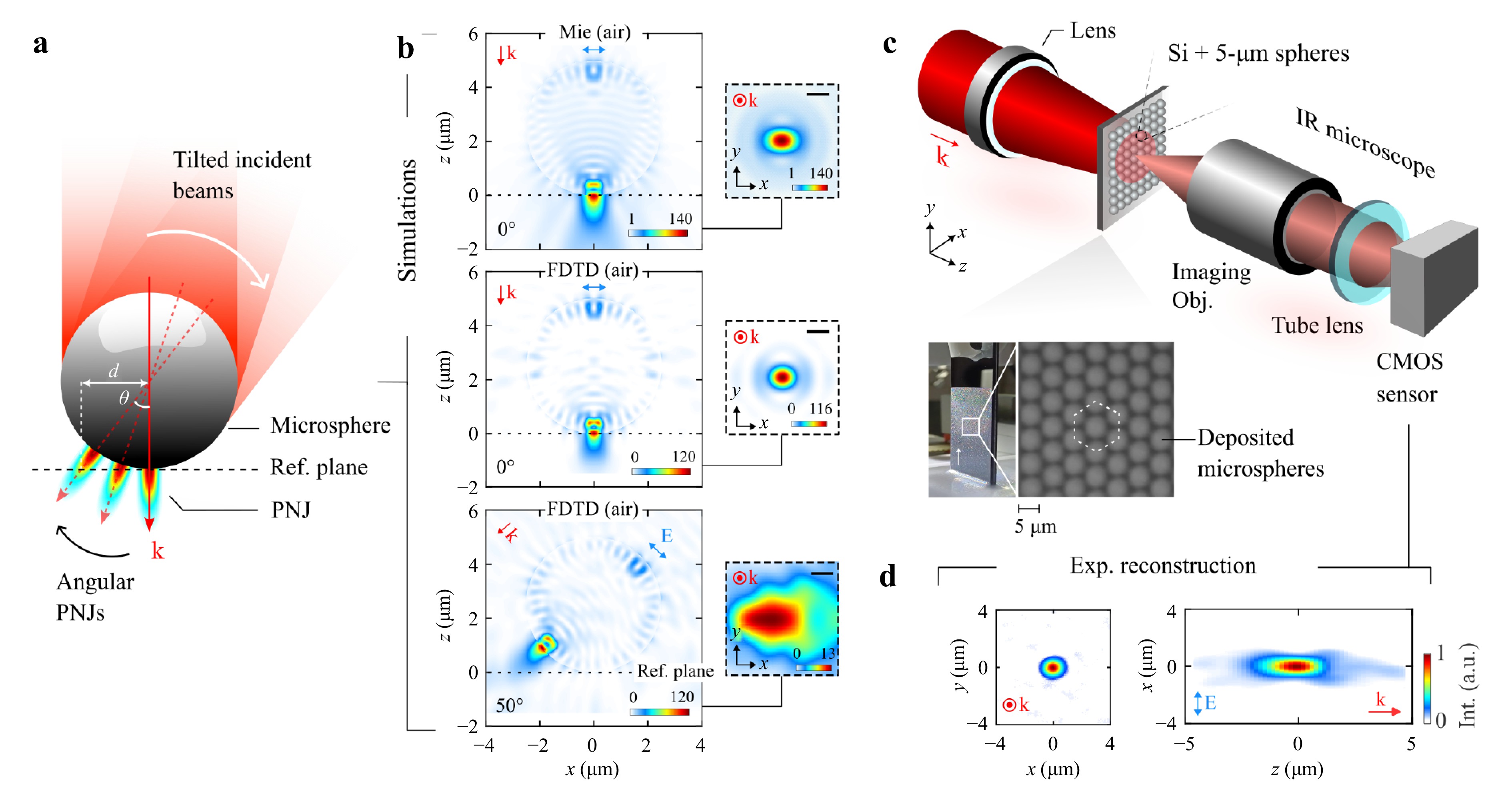
Fig. 1 Generation of photonic nanojets (PNJs) in air using 5 $ \mu $m diameter polystyrene microspheres. a Schematic of PNJ steering via variable-angle illumination, where k denotes the light propagation direction, the white arrow indicates increasing incidence angle $ \theta $ relative to the surface normal, and $ d $ represents the lateral displacement of the PNJ on the reference plane marked by a dotted line. b Cross-sectional intensity distributions along the propagation of PNJs simulated for 0° and 50°, respectively, using Mie theory (top) and FDTD method (middle and bottom). Insets show transverse intensity profiles on the reference plane (scale bar is 0.5 µm). c Experimental setup for PNJ reconstruction at $ \theta $ = 0°, with an inset depicting a Langmuir-Blodgett (LB) film monolayer after sphere deposition; the white arrow indicates the sample lift-off direction during the LB process. d Measured transverse intensity profile (left) at the axial peak intensity position and longitudinal cross-sectional intensity map of the generated PNJ (shown here for a single sphere).
To look at the situation in more detail, we have first calculated, using analytical Mie theory47, 48, the scattering response of a dielectric microsphere surrounded by air when illuminated by a monochromatic plane wave at 1,030 nm wavelength. This allows systematic investigation of PNJ formation. At fixed illuminating wavelength and refractive index contrast between the sphere and the surrounding medium, microspheres with diameters comparable to or smaller than the incident wavelength exhibit field enhancements that are highly localized at the rear surface, rather than forming a well-defined photonic nanojet22 as needed to intercept the reference plane with tilted irradiations. To ensure the formation of an appropriately propagating nanojet characterized by a high-intensity, sharply confined, and elongated field distribution, we therefore decided to concentrate the analyses on microspheres with a diameter of 5 $ \mu $m, which are composed of polystyrene with a corresponding refractive index $ n\sim $1.5749. Although larger microspheres could, in principle, generate even more elongated nanojets, these would directly affect the achievable processing density. The choice of this sphere diameter is then made, looking for a trade-off between appropriate nanojet characteristics and miniaturization for high-density processing capabilities.
In Fig. 1b, we show the simulated longitudinal and transverse intensity distributions on the reference plane (inset). The Mie calculation in Fig. 1b (top) confirms the formation of a tightly confined field near the rear surface of the sphere, featuring a peak intensity (field intensity $ \propto E^2 $) of about 140 times higher than the incident one. Under normal incidence, it exhibits an elliptical transverse profile in the reference plane with a size of FWHM(x) = 0.6 µm and FWHM(y) = 0.43 µm, as directly attributed to the polarization state of the incident light (along $ x $, indicated by the blue double-sided arrow). The longitudinal intensity decay length at $ 1/e $ is $ \approx 0.72\; $µm, corresponding to 0.7$ \lambda $ in air. The angle-dependent intensity distributions in the reference plane from Mie theory are given in the Supplementary Information. As can be guessed from Fig. S1, the shifted spots progressively enlarge, and the intensity vanishes when increasing the incidence angle.
-
Although Mie theory offers an exact analytical solution for the scattering of electromagnetic fields through perfectly spherical particles in a homogeneous, infinite medium, limitations remain in describing conditions in the context of surface laser processing. In particular, it does not account for the presence of a substrate beneath the particle, which can introduce retro-reflected field components. In addition, it cannot describe potential deviations from the ideal spherical geometry (e.g., particle deformations, size variations, and/or surface roughness). To treat these questions, we turn to the Finite-Difference Time-Domain (FDTD) method using commercial software (Ansys-Lumerical). First, to validate the calculations, we have repeated the simulation for normal incidence in air (Fig. 1b (middle)) and compared it to the results obtained using Mie theory (Fig. 1b (top)). Although small differences can be noted, we observe that the characteristics of the field distributions remain very similar with the two calculation approaches, showing that the essential contributions to PNJ formation are correctly accounted in the numerical model. Repeating rigorously the same FDTD calculations for the case of oblique illumination (50° incidence angle), we confirm, with Fig. 1b (bottom), a simple rotation of the intensity distribution, except for a slight symmetry-breaking effect in the inner region of the intense field at the sphere’s exit. The latter is attributed to modest numerical artifacts introduced by finite simulation domain boundaries with perfectly matched layer (PML) conditions, which are no longer oriented along the incident wave propagation. This simulated case directly shows that with increasing angle, the peak intensity on the reference plane gradually decreases (inset), as the separation between the sphere and the reference plane along the path of the incident light increases. For the considered angle, the peak intensity nearly decreases by one order of magnitude, and the spot size largely increases because of the PNJ divergence effect. After repeated simulations, one can note that the graphical distortion in the transverse profile presented in this figure is partly attributed to numerical boundary effects. The distance separating the sphere exit where forms the PNJ and the reference plane, depending on the angle $ \theta $, is expected to follow the expression43
$$ l \approx a\times\left(\dfrac{1}{\cos\theta}-1\right) $$ Then the comparison of $ l $ with the length of the PNJ can be used to describe the practical possibility for surface processing depending on angles. With the considered case at 50°, it is interesting to note that this expression leads to 1.4 µm, largely more than the sub-wavelength jet extension mentioned above (at $ 1/e $). However, given the extremely high maximum field enhancement at the sphere exit (>110), we show that at this distance a hot spot, while larger persist with an intensity more than one order of magnitude higher than the incident intensity and so reasonably high enough for local and selective material surface processing.
Besides these detailed theoretical analyses, direct observation of the PNJ generated by a 5 µm-diameter microsphere under normal incidence remains essential to confirm conditions accessible with experimentally available microspheres. The methodology used for nanojet reconstruction is schematically shown in Fig. 1c and is described in more detail in Materials and methods section. A representative image of the sample immediately after microsphere deposition on a transparent substrate using the Langmuir-Blodgett film method is shown in the inset of Fig. 1c. This image enables a visual assessment of the monolayer coverage, while the magnified microscopy observation confirms an ordered hexagonal close-packed arrangement of the microspheres (see the Sample preparation subsection of Materials and methods for details). The photonic nanojet was experimentally characterized by z-scanning observations (with a step size of 200 nm) of the sample back-side irradiated with the 1,030 nm laser using a high-NA microscopy system. The reconstructed $ x{\textit{z}} $ cross-section intensity profile obtained from the processed image stack is presented on the right side of Fig. 1d, while the corresponding nanojet lateral intensity profile at the best focal plane (highest intensity) is shown on the left. The full width at half maximum (FWHM) extracted from the spot profile is approximately 0.9 µm and the axial decay length is found to be nearly 1.2 µm. This is larger than the simulated values ($ \approx 0.5\; $µm spot size), but the difference corresponds well with the spatial resolution of the imaging system used for this measurement (lateral resolution $ \approx $ 0.67 µm). To address this resolution limit, we have convolved the FDTD-simulated intensity distribution with a Gaussian point-spread function representing the lateral resolution of the experimental imaging system. After applying this filtering, the simulated spot size becomes comparable to the experimentally reconstructed spot size (intensity distributions are shown in Fig. S2 of the Supplementary Information). This agreement indicates that the apparent discrepancy between the raw FDTD simulation and the experimentally reconstructed image is primarily caused by the finite spatial resolution of the imaging system, rather than by a perturbation in the underlying nanojet formation mechanism. The observation of well-defined PNJs and good correspondence between the simulations and measurements also confirms the possibility to work with close-packed arrays of microspheres without noticeable changes in comparison to the case of a single microsphere.
-
A major difference between all previously considered cases and a practical configuration for a material processing application is the presence of the substrate. In practice, we intend to work with the photonic nanojet (PNJ) generated at or near the sphere and substrate interfaces and propagating into the substrate. Fig. 2a, b present the simulated intensity distributions of the PNJs in the $ x{\textit{z}} $ plane for normal (0°) and oblique (50°) incidence, respectively, in the presence of a silicon (Si) substrate. In comparison to previous simulations, we note that the introduction of the substrate significantly modifies the obtained field, leading to a reduction in the apparent PNJ peak intensity. For normal incidence, the apparent peak intensity inside the substrate decreases in comparison to the nanojet formed in air, but we also observe a significant increase in the propagation distance due to the high refractive index of silicon ($ n= $ 3.56). In contrast, at 50° incident angle, because the PNJ is detached from the substrate, the reduction is much less pronounced. The peak intensity enhancement drops by $ \approx 13\% $ compared to an air-standing particle (Fig. 1), but the overall distribution apparently remains very similar, with the exception of a slightly more distorted profile caused in this case by an optical cavity effect. The optical cavity, in the present system, refers to the local air gap formed between the microsphere and the Si substrate at the position where the photonic nanojet interacts with the surface under oblique illumination.
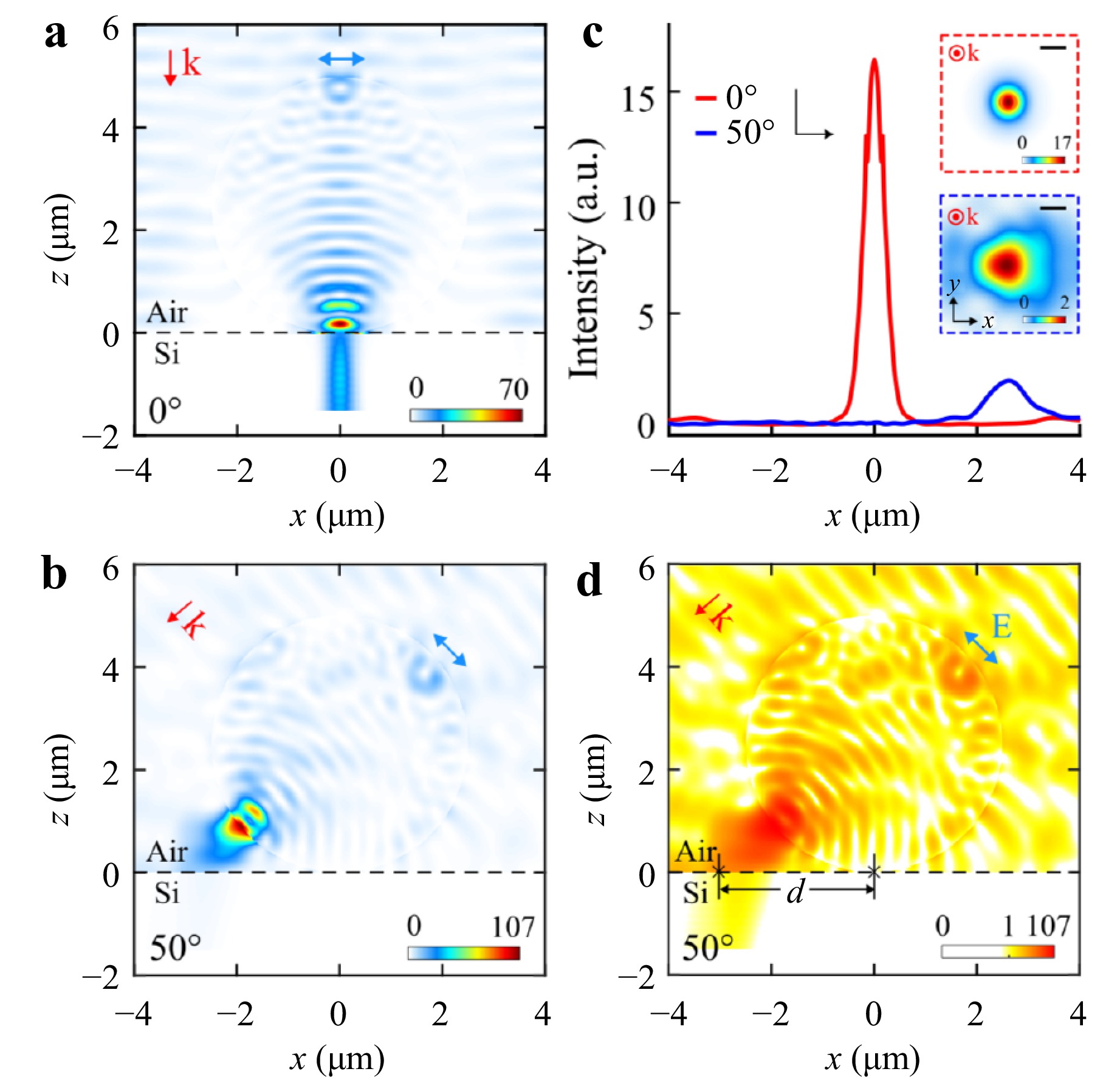
Fig. 2 Effect of substrate on steered photonic nanojets. a, b Intensity distributions of PNJ through a dielectric microsphere positioned on a silicon substrate in the $ x{\textit{z}} $-plane for incident angles of 0° and 50°. The blue arrow indicates the polarization orientation of the incoming optical field. c Transverse profiles of the PNJs at the substrate surface along $ x $, with corresponding transverse intensity maps in the inset (scale bar is 0.5 $ \mu $m). d Longitudinal cross-sectional profile (in the $ x{\textit{z}} $ plane) of the PNJ for a 50° incident angle, displayed on a logarithmic intensity scale.
When the intensity is monitored in the substrate plane (in practice 9 nm below the surface to avoid discontinuities in the simulations50, 51, 41), we obtain the transverse intensity profiles along the $ x $ direction and the corresponding transverse intensity maps (inset) shown in Fig. 2c. For normal incidence, it is striking to observe a more symmetric spot due to a spatial filtering effect caused by the highly reflective surface crossed by wide-angle light components, but it is also interesting to notice a peak intensity on the substrate plane, which drops to approximately 17 times the incident field intensity, highlighting the strong influence of the substrate on energy redistribution near the interface. For 50° incidence angle, the spot enlarges, while the peak intensity enhancement decreases to approximately 2 times the incident field intensity due to the increased separation $ l $ between the sphere and the substrate. Fig. 2d presents the same $ x{\textit{z}} $ distribution for oblique incidence with the intensity presented on a logarithmic scale. This reveals that despite a largely reduced enhancement at high angle, the PNJ remains, in principle, sufficiently intense to enable localized substrate modification under appropriate irradiation conditions. Another interesting observation with this presentation is the location of maximum intensity, shifted in comparison to the expected geometrical distance $ d $ due to the cavity effect in the gap between sphere and substrate. This additionally enhances the asymmetry in spot profiles as evidenced by the relatively triangular shape of the spot (inset in Fig. 2c).
According to these strong effects, FDTD simulations are then conducted to fully investigate the angular dependencies of photonic nanojets. The simulations of angularly scanned PNJs through microspheres directly support the possibility of achieving parallel laser writing over relatively large regions under the spheres. However, important variations of PNJ characteristics can limit uniform writing performance. Fig. 3a shows the transverse intensity distributions normalized to the overall maximum intensity level for varying $ \theta-\phi $ irradiation incidence conditions. The presentation permits a direct comparison of how the PNJ strength evolves with tilt. In this polar representation, $ \rho $ denotes the radial distance of the peak intensity of the PNJ on the substrate plane from the center of the microsphere, as tuned by changing the angle of incidence. The small white circles indicate the expected geometrical peak positions on the substrate plane ($ d $). Interestingly, FDTD simulations show that the actual PNJ maxima are systematically shifted toward the center from these geometric locations. The variations in radial shift are presented in Fig. 3e. The mismatch arises primarily from the presence of the substrate beneath the microsphere, which modifies the nanojet through interference with reflected light from the substrate interface. Importantly, this discrepancy becomes more pronounced at larger incidence angles (corresponding experimental shifts of the PNJ maxima are shown in Fig. S3 of the Supplementary Information). As the incidence angle $ \theta $ increases, the PNJ peak intensity decreases almost monotonically. In contrast, for a fixed $ \theta $, changing the orientation relative to incoming polarization $ \phi $ produces no significant variation in peak intensity, indicating that the dominant control parameter is the tilt angle (angle of incidence) rather than the azimuthal orientation. Fig. 3c summarizes the variation of the peak intensity as a function of the incidence angle, normalized to the normal-incidence illumination conditions. The trend indicates that introducing a slight tilt of about 5° between the incident beam and the sample surface results in stronger optical enhancement compared to normal incidence. This can be attributed to the lateral displacement of the photonic nanojet from the sphere-substrate contact point under oblique illumination, which creates a small air gap between the sphere and the substrate along the nanojet path. Under plane wave illumination, this system acts as a resonator and further contributes to the field enhancement22. At 5° incident angle, this air gap is apparently optimal to enhance the local field at the substrate plane. At higher tilt angles, the reduction in peak intensity can be, in principle, compensated by increasing the input energy. However, this measure does not compensate for another degrading factor with angle: an increase of the apparent spot size on the substrate. This effect is clearly reflected in Fig. 3b, where each transverse map is normalized to its own maximum intensity level. Fig. 3d quantifies this trend through calculated FWHM along the $ x $ and $ y $ directions. The PNJ spots increase steadily in size as the incidence angle increases. Below $ \sim $30°, the nanojet exhibits slight ellipticity along the $ y $ direction, whereas for angles above 30°, the ellipticity flips and becomes dominant along the $ x $ direction (polarization direction). These gradual distortions of the nanojet profile are key features that ultimately limit uniform writing performance over a wide angular scanning range.
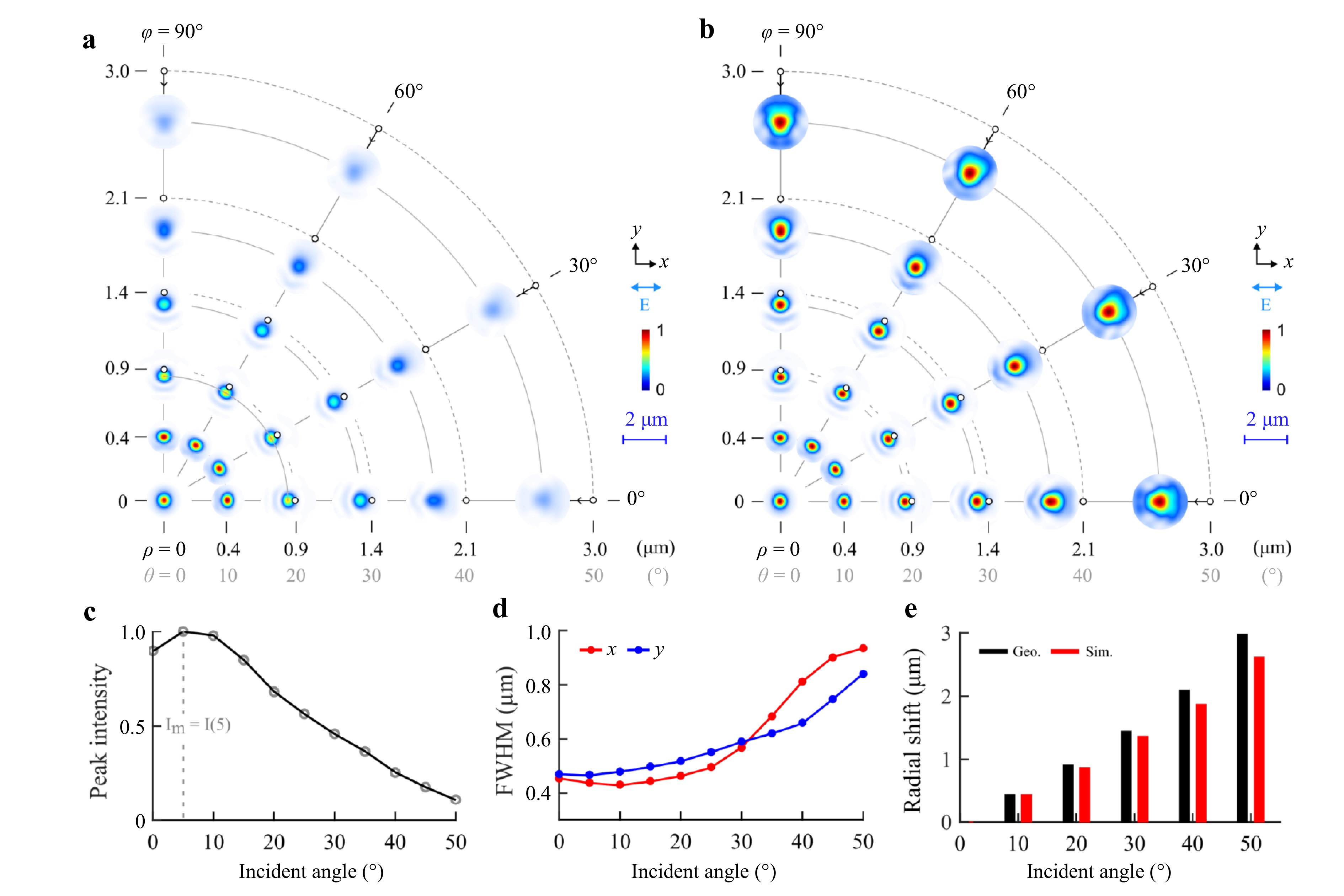
Fig. 3 Intensity profile analysis on substrate surface for varying incidence angles $ \theta $ and $ \phi $, derived from FDTD simulations. a Intensity distributions normalized to the global maximum intensity level. The 2 µm scale bar applies to the transverse intensity maps. b Same intensity distributions, each normalized to its corresponding maximum intensity. c Variation of the delivered peak intensity with increasing angle of incidence at a fixed incoming intensity. d Corresponding changes in the full width at half maximum (FWHM) of the PNJ along the x- and y-directions. The solid curves in both c and d are interpolated from the calculated data points, represented by circles. e Radial shift from the center as a function of the incident angle, compared between simulation results and pure geometrical considerations.
To validate the numerical observations, in Fig. 3a-d, we have performed systematic angle-dependent irradiation experiments in the ablation regime on Si supporting a monolayer of microspheres. The analysis of the laser-induced surface features provides indirect information on the near-field intensity distribution. This characterization is inherently limited, since it relies on the final material modification. However, it remains one of the few experimentally accessible methods for mapping field distributions in such configurations52. Fig. 4a presents SEM images of laser-written features with single-shot irradiation through microspheres (setup illustrated in Fig. 7) for incident angles ranging from 0° to 50° ($ \phi=0 $), while the pulse energy is kept fixed at 2 times the ablation threshold at normal incidence ($ E_{th} $(0°) = 0.05 mJ). At normal incidence, the nanojets generate strong modifications, confirming strong local enhancement beneath the spheres. However, as the incident angle increases, the modification progressively vanishes due to decreased peak intensities reaching the surfaces down to under-threshold conditions at 50° and above. These observations correspond well with the profiles simulated in Fig. 3a. The apparent orientation of the processed features shown in the SEM images is different from the orientation of the calculated intensity profile, since the images are rotated to present a consistent hexagonal microsphere array across all angles. Therefore, the ellipticity of the modified zones does not directly correspond to the experimental ellipticity induced by the incident beam.
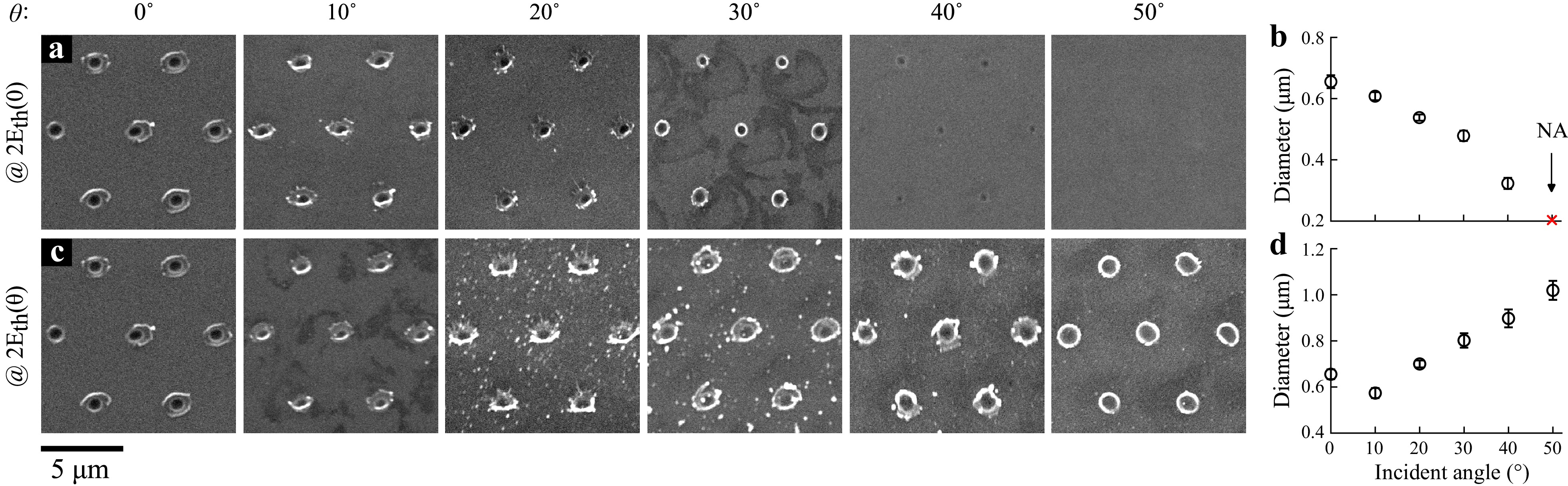
Fig. 4 Ablation behavior of Si under steered PNJ irradiations with single femtosecond laser pulses. a Ablation patterns with irradiation at energy fixed at 2$ \times $ the ablation threshold for normal incidence $ E_{th}(0) $, shown for varying angles of incidence. b Scatter plot showing the reduction in modification size with increasing incidence angle. c Ablation patterns with irradiation at different energies taken at 2$ \times $ the ablation threshold for different angles of incidence, $ E_{th}(\theta) $. d Scatter plot demonstrating the increase in modification size with increasing incidence angle under these conditions.
As for the simulations presented in Fig. 3b, to compensate for the intensity decrease with angle, the pulse energy can be increased. The SEM images of modifications presented in Fig. 4c correspond to irradiations all performed with a pulse energy at $ 2E_{th}(\theta) $, where $ E_{th}(\theta) $ is the experimentally measured ablation threshold (first detectable surface ablation under optical microscopy) found at the different tested incidence angles. With these peak-intensity compensated conditions, laser-induced modifications interestingly reappear with similar contrasts across the full range of tested angles, demonstrating a correct estimation of the required irradiation conditions. However, the compensation results in less confined modifications at higher angles, confirming the inherent trade-off between maintaining the same modification regime and achievable precision. Fig. 4b, d represent the measured feature sizes as a function of the incident angles. The modifications at such relatively strong irradiation conditions in the ablation regime are accompanied by significant thermally affected zones (TAZ). As a result, the modification zones appear different from the calculated optical intensity profiles. For this reason, we have focused on the dark central region of the modified zones, which corresponds to pure ablation. For each incident angle, three spots formed under three individual microspheres under the same irradiation condition are analyzed. The reported spot diameter represents the mean value of these measurements, while the standard deviation defines the error bar, indicating modest variations in the spot diameter. The observed decrease or increase in feature size with increasing angle depends on whether the peak intensity is compensated or not. This behavior illustrates practical limitations when aiming at uniform nano-writing by angular steering.
-
Given the angular-dependent properties of PNJs for surface processing, uniform structuring requires a compensation scheme accounting for the relationship between incident energy, delivered peak intensity, and nanojet waist on the surface.
Our model assumes a threshold-like response typical of ultrafast laser interactions with silicon under single-pulse irradiation and/or where incubation effects are negligible. We first consider the peak intensity ratio at the surface between PNJs at angle $ \theta $ and at normal incidence, as shown in Fig. 3c. This defines the gain factor, $ S(\theta $), which quantifies the delivered peak intensity depending on angle and is directly proportional to the incident pulse energy (for constant pulse duration $ \tau $ as in our experiments). This leads to
$$ I(\theta) \propto E(\theta) \times S(\theta) $$ (1) As a simplification, we then model the nanojet intensity distribution on the target using a Gaussian approximation. Although photonic nanojets do not strictly follow Gaussian profiles (Fig. 3), the Gaussian approximation provides a reasonable analytical description of the central lobe governing threshold-based material modification. This leads to
$$ I (r, \theta) = I(\theta) \times \exp\left(-2\dfrac{r^2}{w^2(\theta)}\right) $$ (2) where $ I $ is the peak intensity, $ w $ represents the beam waist at $ 1/e^2 $ of the peak intensity, and $ r $ is the radial distance from the center. Although this analytical Gaussian distribution is useful for illustrating the concept and communicating its broader applicability, the compensation procedure does not fundamentally rely on the Gaussian approximation. Instead, the exact PNJ intensity profiles obtained from the FDTD simulations can be used. The beam waist as a function of angle $ w(\theta) $ can then be readily obtained from the FWHM extracted from simulations at different angles as shown in Fig. 3d (according to $ w(\theta) $ = FWHM$ (\theta) $/$ \sqrt{2\ln2} $).
We now consider the processing of Si surfaces with a peak intensity exceeding the modification threshold for normal incidence by a factor $ \alpha $, that is $ I(0) = \alpha I_{th} $. Then, according to a threshold-based material response, the radius of the modified zone $ r_D $, corresponds to the condition $ I(r_D,\theta) = I_{th} $. Using Eq. 2, this corresponds to a processed zone with a diameter given by,
$$ D(\theta) = 2w(\theta)\sqrt{\dfrac{1}{2}\ln\left(\dfrac{I(\theta)}{I_{th}}\right)} $$ (3) At normal incidence, substituting the value of $ I(\theta) = I(0) $, we get the processed zone diameter for normal incidence as follows,
$$ D(0) = 2w(0)\sqrt{\dfrac{\ln(\alpha)}{2}} $$ (4) Then, to ensure consistent uniform processing with a modification diameter which becomes invariant with angle, i.e., $ D(\theta) = D(0) $, these considerations lead to a condition for the applied intensities that can be expressed as,
$$ \dfrac{I(\theta)}{I(0)} = \alpha^{\left(\tfrac{w^2(0)}{w^2(\theta)}-1\right)} $$ (5) and thus, according to the intensity-energy scaling relation in Eq. 1, the corresponding condition on the applied pulse energy depends on angle,
$$ {E(\theta)} = \dfrac{E(0)}{S(\theta)} {\alpha^{\left(\tfrac{w^2(0)}{w^2(\theta)}-1\right)}} $$ (6) Accounting for the elliptical profiles of the photonic nanojets, this expression can simply be translated as,
$$ {E(\theta)} =\dfrac{E(0)}{S(\theta)} {\alpha^{\left(\tfrac{w_x(0)w_y(0)}{w_x(\theta)w_y(\theta)}-1\right)}} $$ (7) To obtain an invariant modification size, this equation indicates that the required adjustment of the applied energy is governed by the balance between angular-dependent field enhancement $ S(\theta $) and spatial confinement $ w_x(\theta)w_y(\theta) $. Directly calculated from equation 7, Fig. 5a shows, depending on processing energy level above the threshold at normal incidence, the energy compensation scaling laws to be applied for the configuration considered in this paper (see previous simulations).
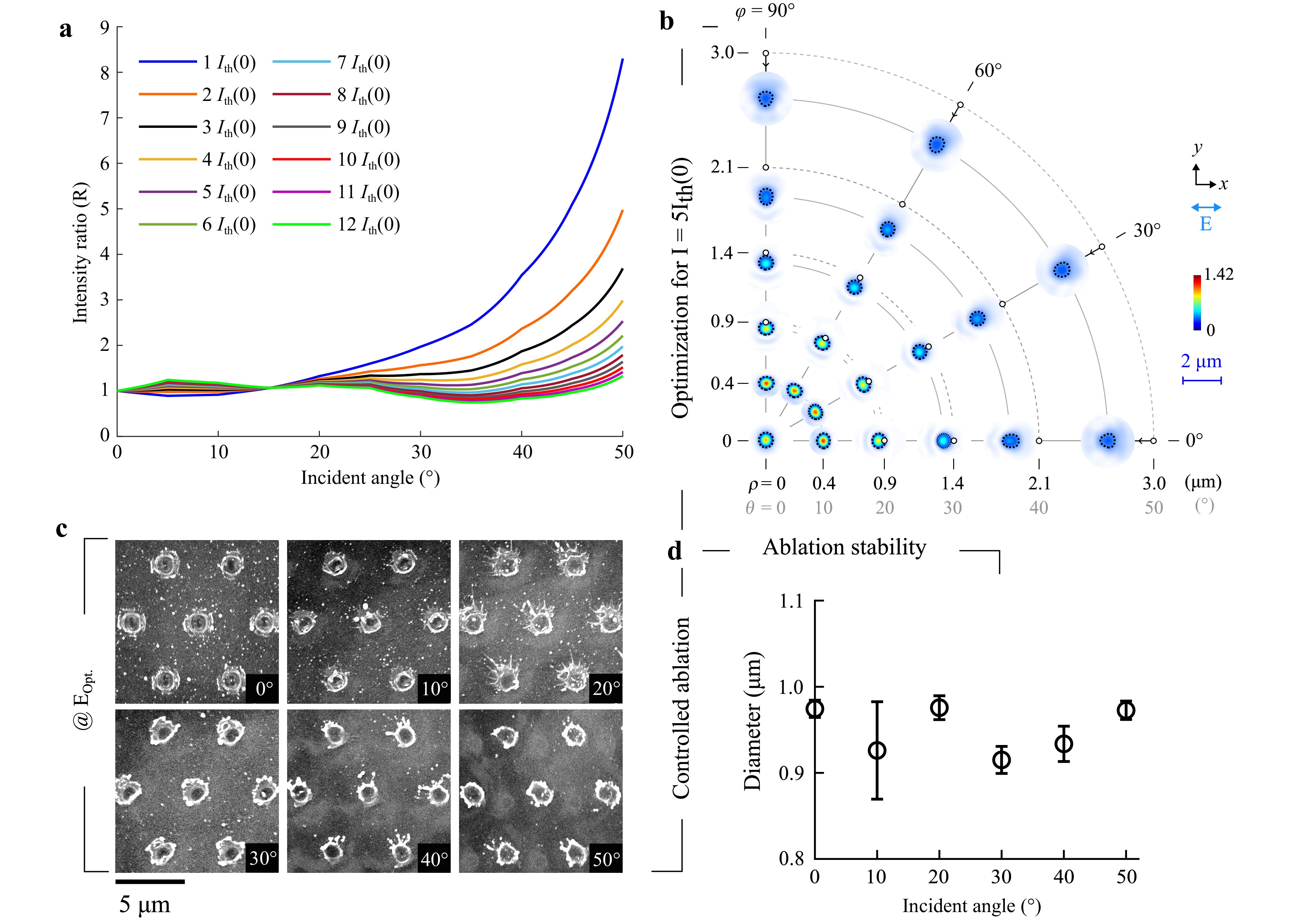
Fig. 5 Compensation of irradiation conditions to achieve uniform surface modifications using steered photonic nanojets (PNJs). a Calculated intensity variations to be applied, depending on the condition above threshold at normal incidence, to maintain stable feature sizes across a range of incidence angles up to 50°. b Optimized transverse intensity distributions applying the compensation displayed in a for processing at $ 5 I_{th}(0) $ beneath the substrate surface. Distributions are shown for varying incidence angles $ \theta $ and orientation $ \phi $ relative to incoming polarization, derived from FDTD simulations and normalized to the normal-incidence case. The 2 µm scale bar applies to the transverse intensity maps. c Post-optimization ablation patterns, demonstrating relatively uniform modification features across all angles. d Measured diameters of the ablation patterns as a function of incident angles, confirming modest variations with the derived compensation measures.
As $ w(\theta)>w(0) $, the waist-dependent term leads to a negative exponent of $ \alpha $ in Eq. 7 such that it acts as an attenuation factor. Then, when processing at near threshold ($ \alpha \sim 1 $), the required energy correction is dominated by the gain factor (1/S($ \theta $)), leading to the necessity for a substantial increase in the applied energy with increasing angles for maintaining a constant feature size. In contrast, for larger $ \alpha $ values, the attenuation term becomes stronger, somehow compensating the gain factor term, resulting in less varying conditions and so the requirement of progressively decreasing energy compensations as can be seen in Fig. 5a. Therefore, one can directly conclude that higher $ \alpha $ values must in principle enable more uniform modifications over a wide range of angles. However, one should not ignore that the required energy level to avoid the need for a compensation is typically one order of magnitude above the material modification threshold (for intensity ratio $ 1\pm0.5 $ according to Fig. 5a). This would immediately lead to largely degraded processing resolutions and precision due to potentially large thermally affected zones. It would basically ruin the benefit of microsphere focusing, an aspect that directly highlights the relevance and importance of the proposed compensation schemes.
To further illustrate the situation with compensated conditions, Fig. 5b shows the corresponding transverse intensity distributions for different incident angles obtained from FDTD simulations, as in previous cases. For the applied energy conditions, we use the scaling law as expressed in Eq. 7, assuming processing intensity fixed at 5$ I_{th}(0) $, obtained from FDTD. The black dotted circles represent the predicted ablation contours corresponding to the intensity level at 5$ I_{th}(0) $, highlighting the expected relatively constant processed area across all tested angles.
Finally, to experimentally validate the robustness of the proposed optimization method, we have irradiated the Si samples at different angles targeting the corresponding processing level of 5E$ _{th}(0) $ at normal incidence. Applying the angle-dependent energy compensation derived in this work, Fig. 5c shows the SEM images of the processed zones. We observe a relatively uniform array of features for incident angles varying from 0° to 50°. The compensation successfully maintains a nearly constant hole size obtained by ablation independently of the incidence angle. The quantitative analysis of the images with error bars standing for the standard deviation of the ablated spots on the images is shown in Fig. 5d. The higher standard deviation observed at an incidence angle of 10° may be attributed to the increased sensitivity of the microsphere-substrate near-field coupling under this irradiation condition. At this angle, the air gap may approach a near-optimal configuration, leading to stronger near-field coupling and enhanced local field intensity at the substrate plane. This enhanced response becomes highly sensitive to small geometrical variations. Given the approximately 8% polydispersity of the microsphere array, slight sphere-to-sphere differences in diameter, shape, and contact geometry can modify the effective air gap, leading to variations in local field enhancement and, consequently, larger differences in the modified features formed beneath adjacent microspheres. However, the extracted feature diameters along $ x $ remain almost constant with angles at a value of $ \approx 0.9\; $µm, a resolution that is directly imposed by the chosen processing level above threshold. Relatively strong conditions are chosen here to simplify the validity demonstration of our method, but this could certainly be improved by setting lower $ \alpha $ values. Interestingly, the presented measurements align well with the expected diameters for varying angles from the simulation in Fig. 5b.
This agreement indicates that, within the experimentally investigated angular range up to 50°, the single-sphere model consistently explains the ideal angular-dependent characteristics of the photonic nanojets despite the monolayer arrangement of microspheres. However, beyond this angular range of illumination, the adjacent microspheres of the monolayer may alter their effective entrance pupils (as shown in Fig. S4 of the Supplementary Information), potentially affecting photonic nanojet properties. Such effects may become non-negligible and should be investigated in future work.
-
For higher-resolution demonstrations, it is more appropriate to work in material phase change regimes that will suppress the thermally affected zones observed in the ablation case. Also, we expect this to ensure conditions that do not cause sphere removal (with the ablated products), which can define a limit for processing by repeated irradiations with steered PNJs under microspheres for massive parallel writing of arbitrary patterns. Despite conditions more difficult to characterize, we have implemented the compensatory measures for real-time surface writing on Si in the surface amorphization regime. In practice, when the Si surface is locally amorphized by irradiations with femtosecond laser pulses, we expect a local increase of the apparent reflectivity (typ. +20−30% depending on amorphization thickness) due to the higher refractive index of amorphous Si compared to the crystalline state53. In this work, we process the sample at $ \sim2 $ times the amorphization threshold of Si under normal incidence to ensure robust modifications while remaining below the material-removal regime. For continuous arbitrary writing, the sample is mounted on a custom gimbal stage arrangement providing two rotational degrees of freedom. Stages are assembled in a eucentric configuration such that the two rotation axes intersect at the laser impact point on the sample surface, allowing repeated single-pulse irradiations of the same zone while varying the incidence angle. The tilt of the sample with respect to the incident beam defines the incident angle $ \theta $, which determines the lateral shift on the surface. The second rotation sets the azimuthal angle $ \phi $ within the sample plane about the impact point. Fig. 6a schematically illustrates the sphere-assisted laser writing mechanism, where each microsphere converts the incident laser beam into a PNJ, formed beneath the sphere. These PNJs behave as writing tips, delivering localized intensity onto the Si surface. By tuning the two rotational angles, the PNJ focus can be steered within the accessible footprint beneath the microsphere. Fig. 6b, c shows arbitrary surface patterns on Si using the proposed sphere-assisted scanning PNJ approach. The left column shows the target patterns, where the yellow cross marks the center of the microsphere and the pink circle indicates the maximum radial displacement reached by the angular tilt. Fig. 6b shows 3 laser-written concentric circles formed at incidence angles $ \theta $ = 15°, 30°, and 45°, from center to radially outward, respectively. For a fixed $ \theta $, the circular trajectory is formed by stepping the azimuthal angle in discrete increments $ \Delta\phi $ between successive irradiations, controlling the spacing and/or overlapping between two modifications. $ \Delta\phi $ is set to 33°, 18°, and 10° for $ \theta $ = 15°, 30°, and 45°, respectively. This simple pattern, written by controlling $ \theta $ and $ \phi $, demonstrates the precise, deterministic control of the dedicated gimbal system for sphere-by-sphere laser processing. However, extending this approach to complex, arbitrary 2D patterning requires a one-to-one mapping between the Cartesian coordinates ($ x,y $) and the angular control variables ($ \theta $, $ \phi $) for the nanojet positioning. Thanks to this transformation, the gimbal stage functions as an angular scanner, allowing it to access any target point within the sphere’s operational range. This mapping enables the introduction of an arbitrary pattern as a pixelated grid with controlled pixel size, and it is implemented by a computer program to automatically control all parameters during laser irradiation sequences. The latter converts the user-defined binary pattern in ($ x,y $) into a sequence of ($ \theta $, $ \phi $), while possibly accounting for corrections on the expected lateral shifts ($ d $) for precise gimbal stage positioning. These aspects are critical for accurate pattern transfer and applying appropriate energy compensation on a pixel-by-pixel basis to maintain uniformity across the written area. In Fig. 6c, a binary pattern with a total size of 4.5 × 4.5 µm2 and a pixel size of 0.5 µm is used. The corresponding optical images compare three different writing conditions from left to right: (i) a fixed pulse energy, about 5% above the amorphization threshold of Si ($ E_{th}(0) $) for normal incidence (at the detection limit); (ii) varying pulse energies, 5% above the amorphization thresholds of Si ($ E_{th} $($ \theta $)) for each angles; and (iii) the optimized energy $ E_{opt.} $, obtained from the compensation model. Without optimization, tilted writing produces incomplete and/or non-uniform features due to the strong angular dependence of the nanojet properties. In contrast, applying the optimization energy scaling results in relatively well-defined and uniform patterns with a 5 µm pitch across the entire accessible region, confirming stable writing performance. While the concentric rings in Fig. 6b at optimized energy directly demonstrate the processing ability to work at ~460 nm precision level (at the resolution limit of these optical observations) with negligible scattering contributions from close-packed microspheres even at higher angles, the patterns in Fig. 6c demonstrate the flexibility of the method for complex, arbitrary writing enabled by automated coordinate mapping and energy compensation. In the above arbitrary writing experiment, however, the spatial lateral offset has not yet been compensated, and the patterns are generated based on the nominal position of the focusing spot. As a result, small deviations between the designed and written patterns may occur, highlighting the importance of incorporating lateral-shift correction in future implementations for more complex patterns.
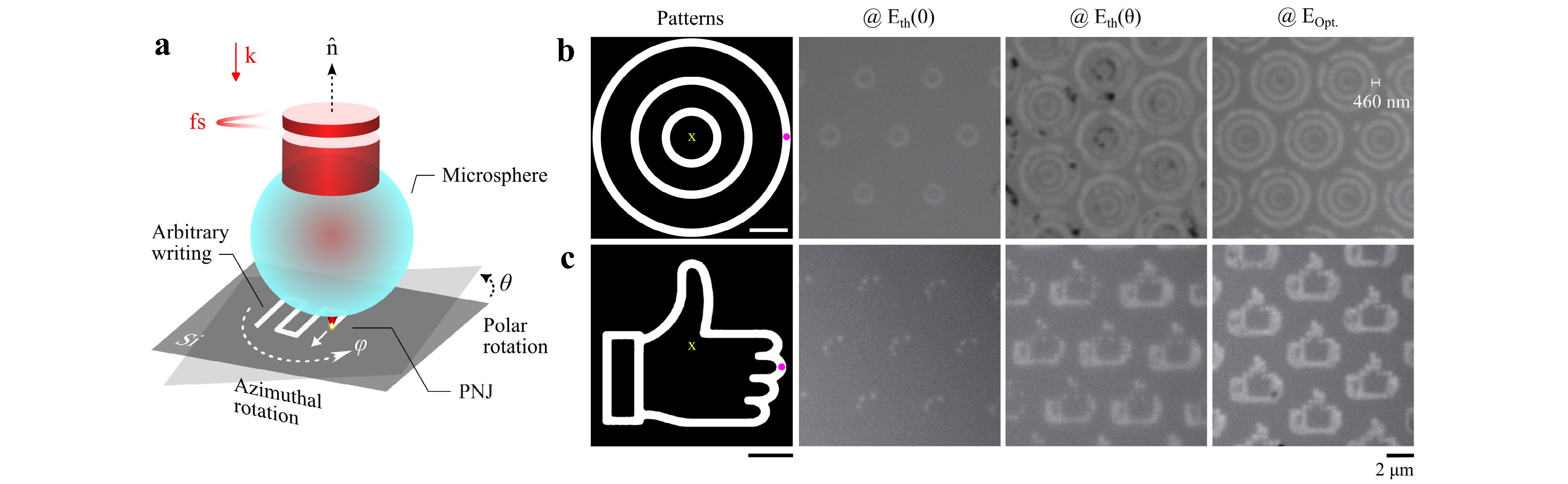
Fig. 6 Demonstration of sphere-assisted laser writing using steered photonic nanojets. a Schematic of the laser-writing configuration utilizing a stable photonic nanojet (PNJ) formed beneath microspheres, with controlled sample motion in $ \theta $ (tilt) and $ \phi $ (azimuthal rotation) for scanned processing. b, c Representative examples of arbitrary laser-written patterns (scale bars are 1 µm) and their corresponding modification images obtained in the amorphization regime of silicon (Si) under varying processing conditions: with and without the proposed compensation measures.
The optical images provide clear evidence of controlled pattern formation over large areas; however, their spatial resolution is not sufficient to accurately determine the feature size of the processed regions. Therefore, additional high-resolution characterization is required. In the phase-transformation regime, feature size estimation is particularly difficult because the laser-modified regions exhibit weak surface contrast. So, a Si sample is further processed near the ablation threshold. Under these irradiation conditions, multiple closely spaced modification sites are generated beneath individual microsphere positions (as shown in Fig. S7 of the Supplementary Information). Although the ablation regime feature introduces thermally affected zones that make the overall modified area appear larger, the dark central ablated regions provide a clearer estimate of the localized modification size. The individual features are found to have a characteristic lateral size of approximately 400 nm. Since ablation typically produces larger apparent modification zones than lower-energy phase-transformation processing, this value provides an estimate of the sub-diffraction feature size of the processed arbitrary patterns.
In addition, to support the physical nature of the laser-induced modifications, Raman spectroscopic measurement on the processed sample in Fig. 6c, has been performed. As shown in Fig. S5 of the Supplementary Information, the spectrum acquired from the unmodified region (red cross) exhibits a sharp peak of crystalline Si at ~520 cm−1. In contrast, the modified zone (blue cross) shows a spectral broadening and emergence of a broad band in the 400−500 cm−1 range (in the inset of Fig. S5), revealing a Raman signature of amorphous Si54. This evolution confirms the localized phase transformation from crystalline to amorphous Si. Although the combined SEM and Raman results demonstrate that the proposed approach enables precise, periodic, sub-diffraction-limited writing through controlled amorphization of the Si surface, FIB-SEM analyses of arbitrary patterns written at the highest resolution level (shown in Fig. S6 of the Supplementary Information), reveal that uniform writing remains challenging. The advanced material analyses evidence residual ablation and/or hydrodynamic flow causing nanometric morphology changes (below 20 nm). Together, these results show that further optimization is needed for fully uniform writing at this scale.
-
In this work, we advance the field of sphere-assisted laser writing by introducing new degrees of flexibility and controllability with an angular scanning approach using photonic nanojets (PNJs). By addressing the limitations caused by peak intensity reduction, the increase of PNJ waist due to its natural divergence at the sub-micron scale, and the cavity effects under the spheres affecting its propagation, we demonstrate that appropriate compensations on irradiation conditions can be applied depending on the applied incidence angles to maintain consistent modification sizes.
The proposed methodology is shown to be valid by experiments in the ablation regime of Si using 5 µm spheres irradiated by femtosecond laser pulses. This can be interpreted as evidence of a material response, well described by a strict-threshold based behaviour, even for sub-micrometer irradiation, as this constitutes the foundational hypothesis to build the calibration model for real-time compensation during nanoscale machining through microsphere-assisted procedures. However, despite this improvement, arbitrary patterning remains challenging due to practical constraints. At high fluences, mechanical recoil and ablated material ejection may lead to sphere displacement or removal, defining the practical upper power limit for microsphere-assisted processing. However, it should be noted that this limit also depends on the irradiation angle. At larger incidence angles, the peak intensity delivered to the substrate is generally lower due to the angular shift and redistribution of the photonic nanojet, allowing the microsphere assembly to tolerate relatively higher irradiation conditions without significant sphere removal or instability. In contrast, near-normal incidence, the photonic nanojet delivers a stronger and more localized peak intensity to the sphere-substrate interface, inevitably increasing the probability of ablation-mediated microsphere detachment and debris/defect formation. Therefore, for large-area processing under each microsphere, the writing sequence should be designed to start from larger incidence angles and finish near the central region. This strategy allows the broader angular range to be processed while minimizing premature microsphere removal. Therefore, even in the ablation regime, the substrate can be processed over a large range of irradiation angles through repeated exposures, only when the writing sequence and angular exposure are properly managed (as shown in Fig. S7 of the Supplementary Information).
Despite this, to mitigate the risk of sphere removal for massive parallelization, we further investigated the amorphization regime for surface writing, where sphere stability is improved. Importantly, the results confirm that the proposed energy compensation strategy remains robust not only in ablation but also in the amorphization regime, reinforcing its broader applicability.
Overall, along with these optimizations, sphere-assisted laser writing has strong potential to become a reliable method for massively parallel surface patterning with sub-diffraction-limited resolution. Relying on the mJ-class laser system used in this setup and writing conditions at $ \approx 200 $ mJ cm−2 for Si amorphization, we can directly extrapolate centimeter-scale beams can be used to create PNJs from a close-packed microsphere monolayer with a 5 µm pitch. This enables more than 106 parallel writing of nanoscale features with pattern flexibility, making the approach highly relevant for future applications in micro- and nanophotonics, metasurfaces, and related surface-structured technologies. In the present implementation, however, the overall throughput is partly limited by the angular scanning speed of the rotational stages. This limitation is technical rather than fundamental. Replacing the rotational stages with a two-dimensional galvo scanner, while maintaining the same laser repetition rate and illumination area, would substantially reduce the angular addressing time and further increase the processing throughput. Therefore, although the current configuration already demonstrates the potential for highly parallel wafer-scale processing, faster beam-steering methods provide a clear route toward high-throughput manufacturing (detailed explanations are given in the Supplementary Information).
Beyond fabrication, the same microsphere-based configurations also provide powerful imaging and sensing capabilities21, 55, 56. This dual functionality allows envisioning the direct creation of optimized nanosystems through the sphere monolayer via laser processing, without requiring sphere removal, enabling efficient collection of optical signals generated or manipulated by the nanosystems. Such integrated capabilities must open promising avenues for the development of highly efficient sensing technologies.
-
The Langmuir-Blodgett (LB) thin-film deposition method is employed to prepare ordered monolayers of microspheres over large substrate areas by enabling controlled transfer of microspheres from an air-water interface to solid surfaces. 380 µm thick, 2 × 4 cm2 Si(111) samples are cleaned via ultrasonication in acetone, followed by rinsing with deionized water. A dilute suspension of polystyrene microspheres (Micromod, 5 µm in diameter, 8% polydispersity) in ethanol is spread onto the water surface. For a close-packed monolayer, the LB deposition is performed at constant surface pressure under ambient conditions, with a controlled substrate withdrawal speed using a commercial automated system (KSV-Nima). This approach results in the formation of highly ordered uniform monolayers of microspheres (inset of Fig. 1c) with approximately 98% coverage and a hexagonal arrangement57. Such a well-defined assembly of microspheres plays a pivotal role in enabling subsequent laser-assisted parallel surface nano-writing with high uniformity.
-
The irradiation experiments are conducted using a diode-pumped solid-state Yb:KGW ultrafast laser source (Amplitude S-Pulse HP), delivering horizontally polarized 1,030 nm, 480-fs laser pulses (Fig. 7a). The maximum pulse energy, at 1 Hz repetition rate, is $ \approx 0.9 $ mJ. The laser pulse energy is controlled using a combination of a half-wave plate ($ \lambda $/2) and a Brewster polarizer (BP), while single-shot irradiation is achieved with a mechanical shutter. The laser beam is loosely focused onto the sample using a plano-convex lens with a 1-m focal length. The lens position is adjusted so that the sample is placed about 15 cm prior to the geometrical focal plane, producing a defocused spot with a diameter of ~1 mm (at 1/$ e^2 $) on the sample surface.
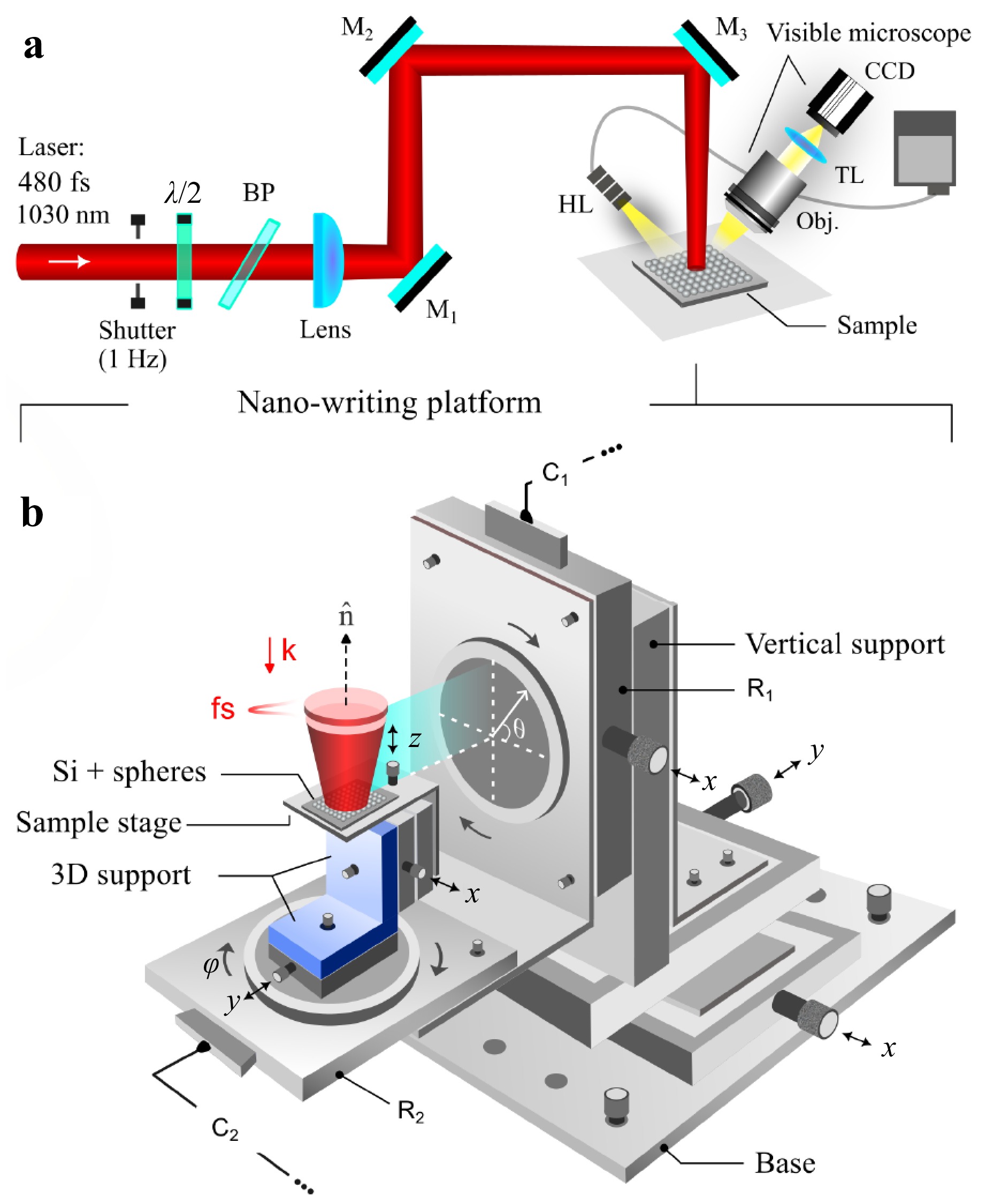
Fig. 7 Experimental configuration for parallel laser nano-writing using steered photonic nanojets. a Schematic of the developed system, integrating an irradiation setup and a reflection microscope for in-situ sample observation and alignments. The white arrow indicates the laser propagation direction. b Detailed 3D-view of the scanning system, with a total of 8 independent control axes. The configuration enables precise irradiation at the exact surface location where the two motorized rotation axes coincide, a critical condition for arbitrary structuring on silicon (Si) using repeated laser pulses through microspheres. The angles $ \theta $ and $ \phi $ define the polar and azimuthal rotations of the sample, respectively.
Prior to the laser irradiation experiments, PNJs are characterized using the reconstruction setup illustrated in Fig. 1c. For this, the prepared sample is oriented such that the beam after passing through the Si-sphere layers (both semi-transparent at the operating wavelength) generates a 2D nanojet array in air. To reconstruct the nanojet field distributions, a 4-$ f $ imaging system is employed, consisting of a microscope objective (Nikon 150$ \times $, NA = 0.95, WD = 0.3 mm), a 200 mm focal length tube lens, and a CMOS camera (Thorlabs DCC1645C-HQ). The imaging module is mounted on a motorized translation stage, enabling axial scanning of the nanojet zone with 200 nm steps. The processed image stack enables the reconstruction of PNJ distributions in three dimensions (Fig. 1d). Potential scattering artifacts or coupling effects from neighboring microspheres, which could alter the field distributions, are shown to be negligible, an aspect further discussed in the Supplementary Information.
The irradiation arrangement for laser direct writing is illustrated in Fig. 7a. The sample is initially aligned perpendicular to the focused beam, which follows a vertical path via dielectric mirrors M$ _1 $, M$ _2 $, and M$ _3 $. The orientation of the sample is kept in such a way that the steered PNJs are formed at the sphere-substrate interface. To enable arbitrary writing beneath each microsphere across a large substrate area with precise control, a custom mechanical system with 8 degrees of freedom is used, as shown in Fig. 7b. The system is equipped with two linear stages ($ X $ and $ Y $) at its base to control the overall lateral position relative to the incident beam. It also features two motorized rotational stages R$ _1 $ and R$ _2 $, where R$ _1 $ allows sample tilt along the z-axis ($ \theta $) and R$ _2 $ enables full 360° rotation in the azimuthal plane ($ \phi $). For fine adjustments, three manual translational stages ($ x $, $ y $, $ {\textit{z}} $) provide independent positioning of the sample, while an additional linear stage ensures that the two rotation axes intersect the beam at a precise position on the sample surface. Alignment procedures are performed using a reflection microscope-equipped with a halogen lamp (HL) for illumination, an objective (Mitutoyo 5$ \times $, NA = 0.14), a tube lens, and a camera (QImaging QICAM), as it is shown in Fig. 1c. Excellent alignment is crucial for optimal writing performance. Under optimized conditions, controlled PNJ steering can be performed with minimal lateral drift ($ \approx 50\; \mu $m) of the incoming beam at the sample surface.
-
Before characterizing the laser-processed surfaces, all dielectric microspheres are removed from the substrate via ultrasonication in acetone, followed by rinsing with deionized water. This removal step is essential, as the presence of spheres obstructs direct optical observation of the laser-modified regions. Following sphere removal, the sample surfaces are optically characterized using an ex-situ commercial optical microscope (NIKON Eclipse LV100ND) in reflection mode with white-light illumination. For high-resolution analysis of surface morphology, the processed samples have been further investigated with scanning electron microscopy (SEM; JEOL JSM-6390). Raman spectroscopic measurements are performed by using a Renishaw inVia Raman microscope, and focused ion beam milling (FIB) of the processed sample is carried out using a HELIOS 5 UC FIB-SEM system from ThermoFisher Scientific.
-
Mie scattering theory48, implemented in Python, is used to simulate the characteristics of photonic nanojets (PNJs) formed in air. Additionally, finite-difference time-domain (FDTD) simulations are conducted using commercial Ansys software to calculate PNJ field distributions at the sphere-silicon (Si) interface. The theoretical formulations and numerical conditions are detailed in the Supplementary Information.
-
This research has been conducted using the LaMP facility at LP3.

 DownLoad: