




-
Silicon carbide (SiC) has emerged as a premier material platform for next-generation integrated photonics, offering a unique combination of a wide bandgap (2.4–3.2 eV)1, large Kerr nonlinearity ($ n_2 \approx 10^{-18}\; {\rm{m^2/W}} $)2, and exceptional thermal conductivity (480 W/mK)3. In contrast to conventional silicon-based platforms such as $ {\rm{Si}} $4, $ {\rm{SiO_2}} $5,6 and $ {\rm{Si_3N_4}} $7−13, SiC also possesses an intrinsic second-order nonlinearity (6.5–12.5 pm/V14), enabling access to both $ \chi^{(2)} $ and $ \chi^{(3)} $ nonlinear processes within the same platform. Moreover, unlike other high-index-contrast nonlinear materials, including $ {\rm{AlN}} $15,16, $ {\rm{AlGaAs}} $17−21, $ {\rm{LiNbO_3}} $22−25, $ {\rm{GaN}} $26,27, $ {\rm{GaP}} $28 and chalcogenide29, SiC is compatible with complementary metal oxide semiconductor (CMOS) fabrication processes, providing a promising route toward wafer-scale manufacturing and integration with electronic components. In addition, its high breakdown voltage ((2–4)×106 V/cm)30 and broad transparency window (0.37–5.6 $ \mu $m)31 make SiC particularly attractive for high-power nonlinear photonics applications.
Despite these advantages, the transition from bulk SiC to a high-confinement, low-loss silicon carbide-on-insulator (SiCOI) integrated platform presents significant manufacturing hurdles. Realising the high-quality-factor ($ Q $) microresonators necessary for nonlinear optical processes demands the mitigation of both material defects and fabrication-induced imperfections. In particular, the scattering loss induced by sidewall roughness becomes increasingly severe in high-confinement submicron waveguides, thereby limiting the achievable $ Q $ factors of SiCOI microresonators32−35. Therefore, the development of advanced thin-film manufacturing and high-precision etching protocols is essential for bridging the gap between raw material properties and functional high-performance chip-scale devices.
One of the most compelling demonstrations of such a high-performance integrated platform is the realisation of microresonator-based frequency combs, or microcombs36,37. High-$ Q $ microresonators facilitate efficient four-wave mixing (FWM), enabling compact solutions for a vast array of applications, including telecommunications38,39, LIDAR40,41, frequency synthesis42, astronomical calibration43,44, and quantum information processing45. The high-index contrast of the SiCOI platform (refractive index $ \approx 2.6 $ at 1,550 nm) enables strong optical confinement and efficient dispersion engineering, which are essential for phase matching in nonlinear processes including FWM46,47, second-harmonic generation48,49, and Kerr comb generation (KCG)50−53.
In this study, we present a comprehensive examination of the SiCOI platform by tracing its trajectory from advanced manufacturing to nonlinear photonic applications. In Section High-Q SiCOI microresonators, we evaluate two distinct 4-inch SiCOI thin-film fabrication methods, namely, ion-cut and bulk wafer-thinning techniques, to analyse how manufacturing choices influence the crystal quality and resonance performance. We also introduce a refined surface-smoothing technique using wet thermal oxidation to achieve sub-nanometre sidewall roughness. In Section Kerr frequency comb in SiC microresonators, we experimentally demonstrate diverse Kerr comb states in both the anomalous and normal dispersion regimes, thereby validating the nonlinear performance enabled by the optimised manufacturing platform.
-
High-$ {{Q}} $ microresonators play a crucial role in achieving low-threshold KCG. However, realising a high-$ {{Q}} $ microresonator that combines the desired dispersion design and strong light confinement is a nontrivial task. On the SiCOI platform, these prerequisites necessitate waveguide design with small cross-sectional dimensions. Fig. 1 provides a guide for selecting appropriate waveguide dimensions for investigation, with the schematic cross-section of the SiCOI waveguide shown in the inset of Fig. 1. It shows the calculated effective mode area (colour-shaded contour) for the fundamental transverse electric mode ($ {\rm{TE_{00}}} $ mode) of SiCOI waveguides with different waveguide dimensions. Additionally, we calculated the waveguide dimensions corresponding to zero-group-velocity dispersion (zero-GVD) for different modes, including $ {\rm{TE_{00}}} $ (solid black), fundamental transverse magnetic mode ($ {\rm{TM_{00}}} $) (dashed red), and higher-order $ {\rm{TE_{10}}} $ mode (dashed blue). The grey shaded region in the lower-left corner indicates a single-mode operation regime.
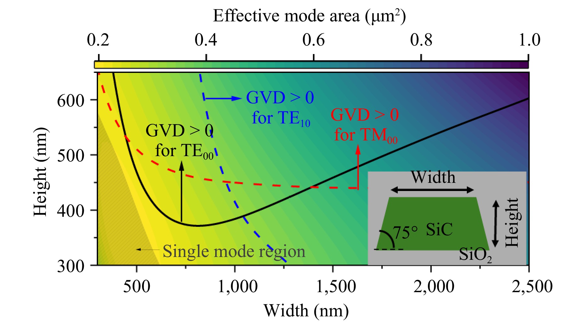
Fig. 1 Calculated effective mode area (colour-shaded contour) and the group velocity dispersion ($ {\rm{GVD}} $) at 1,550 nm for the $ {\rm{TE_{00}}} $ mode (solid black), $ {\rm{TM_{00}}} $ mode (dashed red) and higher-order $ {\rm{TE_{10}}} $ mode (dashed blue) of $ {\rm{SiCOI}} $ waveguides with different cross-section dimensions. The grey-shaded area is the single-mode operation region. The inset shows the schematic cross-section of a $ {\rm{SiCOI}} $ waveguide.
$ {{Q}} $ is determined by both the intrinsic material loss and the fabrication imperfection-induced scattering loss. This section concentrates on the fabrication process and $ {{Q}} $ performance of SiCOI microresonators. Subsection SiC thin-film fabrication methods presents our work on SiC thin-film fabrication using two distinct approaches: the ion-cut and bulk wafer thinning methods. The advantages and disadvantages of these methods are discussed. In subsection Fabrication of SiCOI microresonators, we introduce an optimised device fabrication process that incorporates a sidewall roughness reduction technique via wet thermal oxidation. Subsection Performance of SiCOI microresonators presents the characterisation and comparison of $ {{Q}} $ values for SiCOI MRRs fabricated using different SiC thin-film fabrication methods.
-
We explored two fabrication methods for obtaining a SiCOI stack with a thin SiC film on top. A schematic diagram of the ion-cut method is shown in Fig. 2a54. First, a 4H bulk SiC wafer was implanted with 170 keV $ {\rm{H^+}} $ species. The silicon carrier wafer was thermally oxidised to grow a 2 µm-thick silicon dioxide layer. After cleaning, both the wafers were bonded using molecular wafer bonding. Subsequent annealing at approximately 850 °C facilitated separation of the thin SiC film from the bulk SiC wafer. The split wafer was further annealed at 1,100 °C for 10 h, followed by thinning and planarization of the SiC layer via chemical-mechanical polishing (CMP). Fig. 2c shows a photograph of a fabricated 4-inch SiCOI wafer post-splitting with a thickness uniformity of 4 nm. Although high uniformity is an advantage, the ion implantation step in this fabrication method introduces defects in SiC55,56, leading to extra material loss.
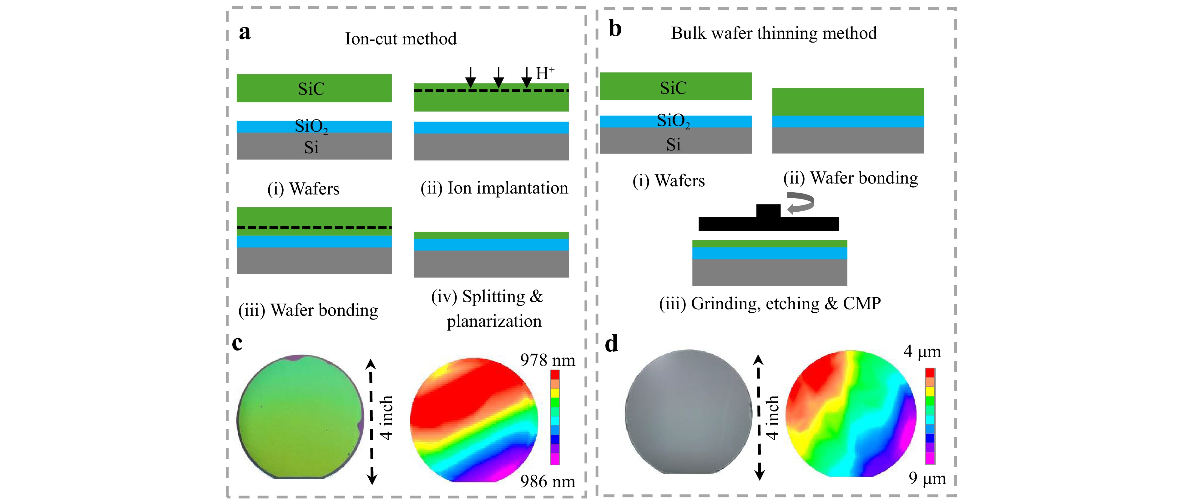
Fig. 2 SiCOI wafer fabrication methods. Schematic drawing of the fabrication process based on a the ion-cut method and b the bulk wafer thinning method. c, d Photos of fabricated 4-inch SiCOI wafers and thickness variation across the wafer based on c ion-cut method and d wafer thinning method.
The second fabrication method is based on bulk wafer thinning35, 48, 51, in which SiC is reduced from 500 $ \mu $m to the target thickness through grinding, etching, and CMP after wafer bonding (Fig. 2b). A SiC bulk wafer was first bonded to a thermally oxidised Si substrate via hydrophilic bonding, followed by annealing at 600 °C in $ \rm N_2 $ atmosphere. After this thermal treatment, the SiC layer was mechanically ground down to 20 $ \mu $m using an 8,000-grit wheel. The subsequent dry etching step further reduced the SiC thickness to 4 $ \mu $m. The bonded stack was then annealed at 800 °C to further enhance bonding strength. Fig. 2d shows a photograph of the SiCOI wafer and SiC thickness variation after the grinding and dry-etching steps. Finally, it was cleaved into small samples and CMP was applied to achieve an atomically smooth surface of the SiC layer. Although this method does not introduce additional material loss, it is challenging to achieve a uniform SiC film at the wafer scale using only the CMP step. To maintain the performance of the targeted device, we mapped the thickness of the SiC layer prior to lithography. The device dimensions were then customised based on this map to compensate for the local thickness deviations.
-
SiC microresonators were fabricated using electron-beam lithography (EBL). A negative resist, hydrogen silsesquioxane (HSQ), was spin-coated on a SiCOI sample as an etching mask and a 20 nm aluminium layer was subsequently deposited to avoid pattern distortion from the charging effect. To mitigate the temporal noise and spatial aberrations in the EBL deflection system, multi-pass exposure was implemented57−59. This approach ensured that each shape was partially written into a different area of the exposure field. Subsequently, the device pattern was transferred onto the SiC layer using an inductively coupled plasma reactive ion etching (ICP-RIE) machine with fluorine-based gases ($ {\rm{SF_6}} $). The etch rate was measured to be 140 nm/min, and the selectivity for the mask was 1.4.
Fig. 3a presents a scanning electron microscopy (SEM) image of the SiC waveguide after etching. As can be seen, the fabrication imperfections lead to sidewall roughness, which induces the scattering loss and compromises the $ {{Q}} $ of microresonators. In this study, we investigated the effects of oxidation on the improvement in roughness. Wet oxidation was performed at 1,100 °C for two hours to oxidise approximately 100 nm SiC. During this process, SiC is thermally oxidised to the form of $ {\rm{SiO_2}} $. Fig. 3b shows an SEM image of SiC after etching and $ {\rm{SiO_2}} $ removal, where only two hours of wet oxidation resulted in a significant improvement in the sidewall roughness. Fig. 3c and 3d illustrate the atomic force microscopy (AFM) of the SiCOI sidewall before and after oxidation, revealing a root mean square (RMS) roughness reduced from 1.73 nm to 0.98 nm.
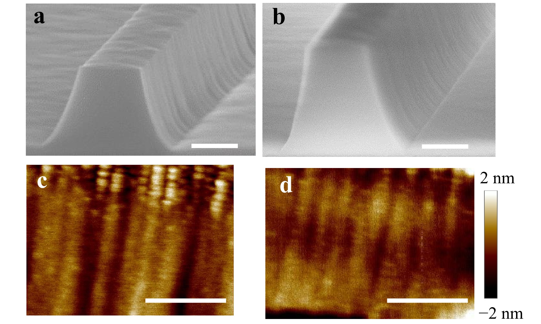
Fig. 3 Sidewall smoothness through wet oxidation. a $ {\rm{SEM}} $ image of $ {\rm{SiC}} $ waveguide after etching. b $ {\rm{SEM}} $ image of $ {\rm{SiC}} $ waveguide after etching and 2-hour wet oxidation at 1,100 $ ^{\circ} $C. $ {\rm{AFM}} $ image of $ {\rm{SiC}} $ waveguide sidewall before c and after d wet oxidation, where the RMS roughness is reduced from 1.73 nm to 0.98 nm. Scale bars indicate 200 nm.
-
Because the $ {{Q}} $ factor serves as a key indicator of microresonator loss performance and strongly influences the efficiency of nonlinear processes, we conducted a comparative analysis of the $ {{Q}} $ factors of SiC microring resonators (MRRs) fabricated using ion-cut and bulk wafer thinning methods.
Fig. 4 summarises the loss performance of SiCOI MRRs fabricated using the ion-cut method. Fig. 4a shows a histogram of the intrinsic resonance linewidth for ten 1-THz MRRs with waveguide dimensions of 750 nm $ \times $ 500 nm and a 75$ ^{\circ} $ sidewall angle, indicating the most probable value of 3 GHz. The inset shows the fundamental TE ($ {\rm{TE_{00}}} $) mode profile of the waveguide. Fig. 4b shows the maximum achieved intrinsic $ {{Q}} $ value of $ 7.3 \times 10^4 $34.
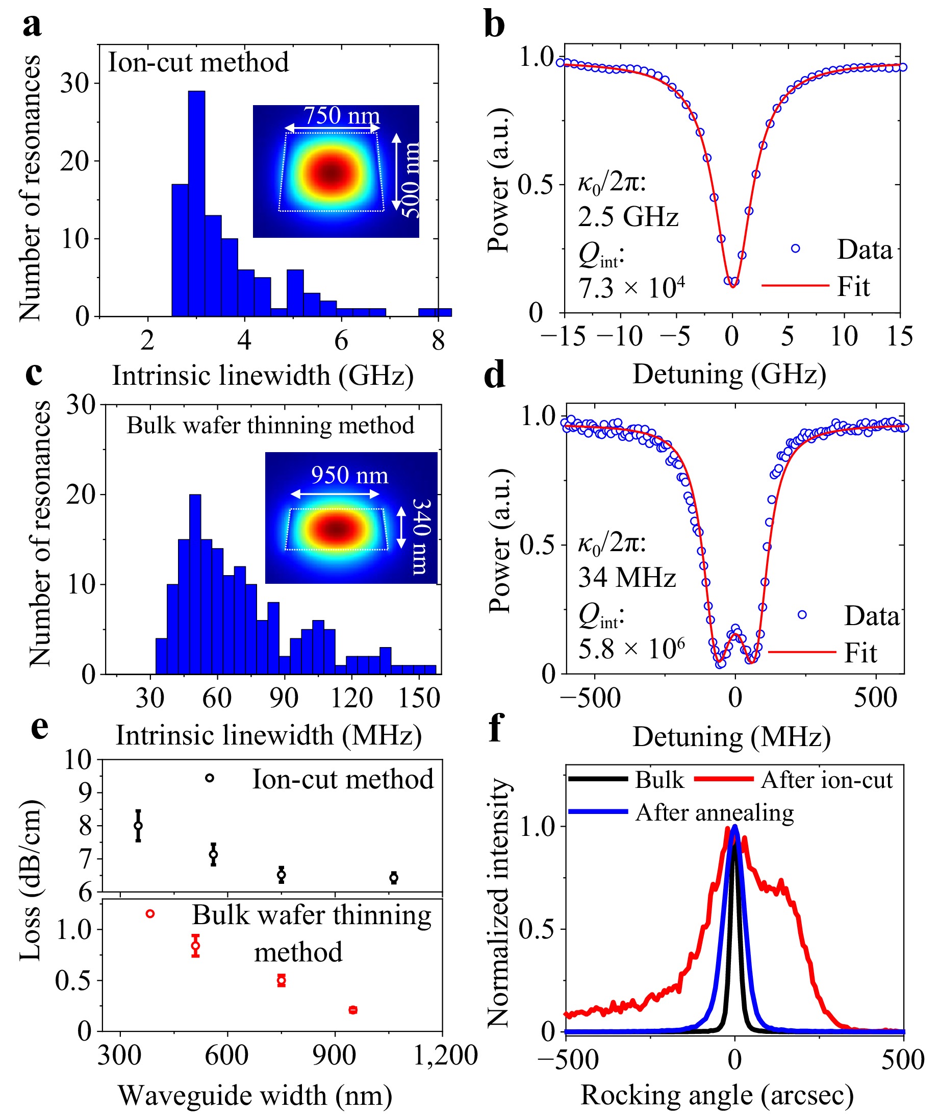
Fig. 4 $ {{Q}} $ analysis of $ {\rm{SiCOI}} $ $ {\rm{MRR}} $s fabricated from the wafer using ion-cut method a, b and bulk wafer thinning method c, d. a, c Histogram of intrinsic resonance linewidth for ten 1-THz $ {\rm{MRR}} $s with the waveguide dimension and $ {\rm{TE_{00}}} $ mode profile indicated in the inset, showing the most probable value of 3 GHz a and 55 MHz c. b, d Measured (normalized) transmission spectrum for a resonance showing the maximum $ {{Q}} $, corresponding to intrinsic linewidth of 2.5 GHz b and 34 MHz d. e Extracted loss for $ {\rm{MRR}} $s with different dimensions. f X-ray diffraction ($ {\rm{XRD}} $) rocking curves for the (black) bulk $ {\rm{SiC}} $ wafer and finished $ {\rm{SiCOI}} $ wafer before (red) and after (blue) thermal annealing.
In SiC thin-films fabricated using the bulk wafer thinning method, the original SiC crystal quality is preserved, albeit with a trade-off, resulting in a nonuniform SiC layer across the wafer. Despite this nonuniformity, a range of 80 nm nonuniformity in a 1 cm $ \times $ 1 cm sample area is achievable50. The same device fabrication steps were performed to ensure that the MRRs from different SiCOI wafers had similar sidewall roughness. Fig. 4c shows a histogram of the intrinsic resonance linewidth with the most probable value of 55 MHz and a maximum intrinsic $ {{Q}} $ of 5.8 million (Fig. 4d), where we adopted a widely used model for fitting the splitting resonances60. Although $ {{Q}} $ is similar to the state-of-the-art value reported by Guidry et al.61, the waveguide cross-sectional dimension is two times smaller (950 nm $ \times $ 340 nm, as shown in the inset of Fig. 4c). Achieving such a high $ {{Q}} $ in high-confinement SiCOI microresonators is nontrivial because of the reduced waveguide dimensions, resulting in a more pronounced light field at the waveguide sidewall and rendering it highly sensitive to sidewall roughness. In addition, strong light confinement results in a smaller effective mode area ($ {A_\text{eff}} $), leading to an efficient KCG.
The propagation loss in high-index-contrast SiCOI waveguides is also influenced by the waveguide width as the light intensity at the $ {\rm{SiC}} $–$ {\rm{SiO_2}} $ interface varies, resulting in different scattering losses with varying waveguide dimensions. To investigate these differences, MRRs with different waveguide dimensions are fabricated. Fig. 4e presents the extracted propagation losses for SiC MRRs with varying widths. Different colours represent different SiC thin-film fabrication methods. It is noted that the SiC thicknesses are 500 nm and 340 nm with the ion-cut and bulk wafer thinning methods, respectively, where the lowest realised losses are 6.4 and 0.2 dB/cm. A loss of more than one order of magnitude underscores the fact that the maximum achievable $ {{Q}} $ is constrained in SiCOI wafer fabrication using the ion-cut method.
To qualitatively study the SiC crystal quality during the ion-cut fabrication process, we use X-ray diffraction (XRD) to characterize the material. The rocking curve of SiC was measured to determine its crystal quality, and the diffracted intensity was recorded while tilting the sample. In Fig. 4f, the black line represents the normalised intensity of the diffracted X-ray signal from the bulk SiC wafer with respect to the rocking angle, indicating the full width at half maximum (FWHM) of the rocking angle at 25 arcsec. After the ion implantation and splitting steps, the FWHM increased to 288 arcsec (red line in Fig. 4f), indicating a significant degradation in the crystal quality of the SiC layer. Such degradation is attributed to the ion implantation step, where a high dose of energetic $ {\rm{H^+}} $ passes through the crystal, causing defects such as dislocations and vacancies55,56. Thermal annealing is a common method employed to recover the crystal quality. The blue line in Fig. 4f illustrates a split SiCOI wafer after thermal annealing at 1,100 °C in an $ {\rm{Ar}} $ environment. The four-fold reduction in the FWHM rocking angle indicates an improvement in the crystal quality of SiC. However, the applied temperature cannot fully restore the crystal because the growth temperature of SiC is 1,700 °C and the buried $ {\rm{SiO_2}} $ and $ {\rm{Si}} $ substrates cannot withstand such high temperatures. Therefore, retaining the original crystal quality of the SiC layer after the ion-cut process is challenging.
-
Table 1 summarizes the critical performance metrics for $ {\rm{SiCOI}} $ platforms fabricated via the ion-cut and bulk wafer thinning methods used in this work. Owing to the high technological maturity of the ion-cut process, film uniformities of $ \pm $(2.5–10) nm can be routinely achieved across 4-inch wafers. However, it was difficult to achieve wafer-scale uniformity using CMP alone when the initial thickness variations were large (Fig. 2d). Current industrial-level services can produce SiC films with $ \pm $(25–50) nm uniformity on 4-inch wafers through specialized trimming treatments62. This significantly reduced the design complexity of large-scale circuits.
Metrics Ion-cut Bulk wafer thinning Wafer uniformity $ \pm $ (2.5–10) nm $ \pm $ (25–50) nm Top-surface roughness $ \lt $ 0.1 nm $ \lt $ 0.1 nm Achieved $ Q_{{\mathrm{int}}} $ $ 7.3 \times 10^4 $ $ 5.8 \times 10^6 $ Cost $ \sim $ $750/wafer $ \sim $ $1,500/wafer Scalability High Moderate Table 1. Comparison of fabricated SiCOI platform using ion-cut and bulk wafer thinning methods in this work.
Although both methods achieve top-surface and sidewall roughness below 0.1 nm and 1 nm, respectively, enabling low scattering loss, the maximum $ Q_{{\mathrm{int}}} $ of bulk-thinned resonators is approximately two orders of magnitude higher than that of ion-cut resonators. This disparity indicates that the residual lattice damage from ion implantation remains a dominant source of optical loss in ion-cut films. To mitigate this issue, elevated implantation temperatures (e.g. $ \sim $600 °C) can be used. Such conditions have been reported to reduce the critical implantation dose by a factor of nearly two, thereby substantially suppressing defect formation46,63.
-
The first KCG in SiCOI MRRs was reported by Guidry et al.50, who utilised the higher-order TE10 mode as the pump mode with an anomalous GVD. Similar results were observed for micro-disk resonators (MDRs) 51. However, the generated combs are noisy. Subsequently, soliton states were achieved in both MRRs and MDRs61,64, which involve either a cryostat environment61 or an auxiliary laser cooling technique64,65. They are both employed to address the challenges posed by the significant thermal effects resulting from high intracavity power. Despite these promising achievements, the soliton bandwidth has remained relatively narrow. The development of a broadband comb with an octave-spanning spectral range, which is a prerequisite for self-referencing, introduces challenges. Careful dispersion engineering is essential because simultaneously maintaining high Q and high confinement performance is required. Although achieving an octave-spanning KCG is successful, the applied high pump power induces severe thermal effects, which makes soliton generation challenging52.
For KCG, the waveguide dimensions are usually designed to exhibit anomalous $ {\rm{GVD}} $ ($ {\rm{GVD \gt 0}} $), as this is a prerequisite for achieving phase-matching conditions for optical parametric oscillation (OPO). However, there have been observations of KCG in MRRs with normal $ {\rm{GVD}} $ ($ {\rm{GVD \lt 0}} $), which is contingent on the presence of avoided mode crossing (AMX). This section discusses the KCG and soliton generation in SiCOI MRRs with anomalous and normal $ {\rm{GVD}} $. Subsection Dispersion engineering of SiCOI microresonators focuses on the dispersion engineering in high-confinement SiCOI waveguides with a low-threshold KCG. In Subsection Dissipative Kerr soliton comb generation, we demonstrate the generation of a broadband soliton microcomb using an experimental laser-cooling technique. Subsection Multi-soliton state and soliton crystal state presents the experimental results for multi-soliton and soliton crystal states. Subsection Soliton burst and bidirectional switching delves into the dynamics of soliton bursts and the bidirectional switching of solitons. In Subsection KCG in normal-dispersion microresonators, we present the KCG caused by nonlinear polarisation mode coupling in SiCOI with a normal $ {\rm{GVD}} $. Subsection Dark pulse Kerr comb in SiCOI microresonators discusses the dark-pulse Kerr (DPK) comb generation in an SiCOI MRR.
-
Dispersion engineering is crucial, because it determines the achievable comb bandwidth. High-index contrast material platforms, such as SiCOI, offer advantages for efficiently manipulating dispersion by controlling the cross-sectional dimensions of the waveguide. Fig. 5a shows an SEM image of the fabricated 1-THz-FSR MRR. Fig. 5b shows the simulated integrated dispersion ($ {D_\text{{int}}} $) of MRRs with different waveguide dimensions, characterised by waveguide height ($ {{H}} $), waveguide width ($ {{W}} $), slab thickness ($ {{h}} $), and sidewall angle $ {\rm{\theta}} $ (inset in Fig. 5b). Here, $ {D_\text{int} = \omega_{\mu} - \omega_0 - D_1\mu = \displaystyle\sum\limits_{n \ge 2} {D_n \mu^n}/{n!}} $, where $ {{D_n}} $ represents the $ {{n}} $th-order dispersion coefficient. The waveguides with cross-sectional dimensions of 950 nm $ \times $ 340 nm (red) exhibited normal dispersion. By adjusting $ {{h}} $ to 100 nm, the dispersion could be manipulated to be anomalous, thereby facilitating the achievement of an octave-spanning bandwidth. This was achieved with the assistance of two phase-matching points (dispersive waves) on both sides of the pump frequency.
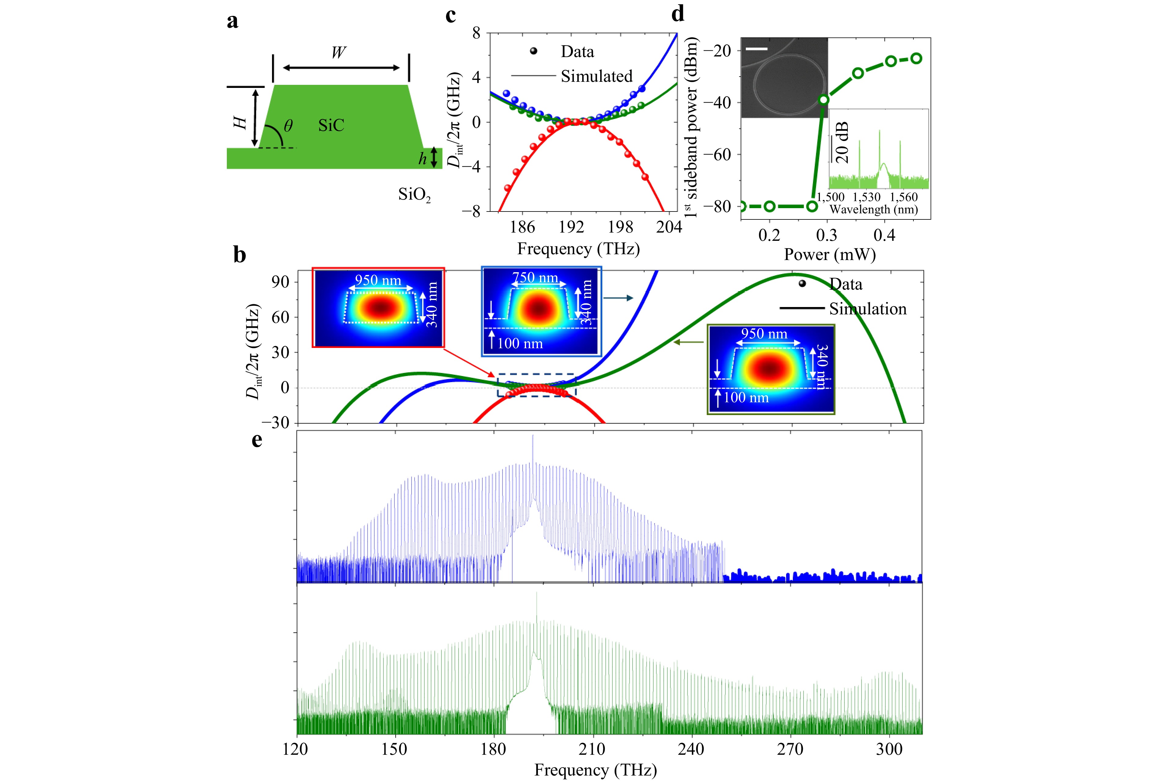
Fig. 5 KCG in dispersion-engineered $ {\rm{SiCOI}} $ microring resonators with anomalous $ {\rm{GVD}} $. a $ {\rm{SEM}} $ image of a 1-THz-$ {\rm{FSR}} $ microring resonator (scale bar: 10 µm). b Simulated integrated dispersion of the $ {\rm{TE_{00}}} $ mode for 16.5-µm-radius waveguides with different cross-sectional geometries indicated by the inset (schematic cross-section of a $ {\rm{SiCOI}} $ waveguide defined by waveguide height ($ {{H}} $), waveguide width ($ {{W}} $), slab thickness ($ {{h}} $), and sidewall angle $ {\rm{\theta}} $). The measured data points of integrated dispersion are shown in the grey dashed box. c Zoom-in of measured integrated dispersion with waveguide geometries in b. d The output power of the first generated $ {\rm{FWM}} $ sideband as a function of coupled power. e Measured spectra for $ {\rm{KCG}} $ in devices with corresponding waveguide geometries in b.
The measured $ {D_\text{{int}}} $ values are presented in Fig. 5c, with the frequency axis calibrated using a free-space cavity with a free spectral range (FSR) of 100 MHz34. By fitting the data, the second-order dispersion ($ {D_{2}/2\text{π}} $) for these three dimensions was extracted as $ - $171.9 (red), 78.08 (blue), and 51.8 (green) MHz at 1,560 nm (the pump wavelength for KCG). Therefore, MRRs with anomalous GVD shown by the blue and green curves, are suitable for KCG. The corresponding intrinsic Q values of devices with different dimensions are 3.5$ \times 10^6 $ (red), 1$ \times 10^6 $ (blue), and 2.4$ \times 10^6 $ (green). We attribute the reduced Q in devices with a slab to the increased bending loss. Waveguides with smaller $ {A_\text{{eff}}} $ contribute to lowering the threshold power for KCG owing to the enhanced effective nonlinearity. Despite the 750 nm-wide MRRs having smaller $ A_{\text{{eff}}} $ (0.38 µm$ ^2 $) compared to the 950 nm-wide MRRs (0.45 µm$ ^2 $), their $ {{Q}} $ values are approximately 2.4 times lower, which is attributed to more scattering loss. Therefore, 950 nm wide MRRs are chosen for OPO and broadband comb characterisation because they exhibit a small anomalous dispersion as well as a relatively high Q factor, which directly influences the threshold power ($ P_{{\mathrm{th}}} $) for comb generation by $ P_{{\mathrm{th}}}\propto1/Q^2 $. In the measurement setup, a pump laser was amplified in an erbium-doped fiber amplifier (EDFA) and coupled to the $ {\rm{TE_{00}}} $ mode of the waveguide through edge coupling. The high Q and relatively small $ A_{\text{{eff}}} $ of the MRR significantly reduce the threshold power to a sub-milliwatt level of 0.29 mW, as depicted in Fig. 5d.
To generate the Kerr comb, the pump power was further increased to 80 mW. The blue spectrum in Fig. 5e shows the comb spectra from MRRs with 750 nm wide waveguides. The generation of only one dispersive wave (DW) limits the bandwidth to less than one octave. In contrast, an octave-spanning comb is obtained when the waveguide width of the MRR increases to 950 nm (green). Such a broadband comb is important for many applications because an octave-spanning comb facilitates f-2f self-referencing, which is essential for comb stabilisation. However, its noisy state makes its practical use difficult.
-
The formation of a dissipative Kerr soliton (DKS) with low noise results from the double-balance loss and gain in the cavity, along with nonlinearity and dispersion. DKS manifests itself when the pump laser is red-detuned from resonance. However, in the context of broadband comb generation, the substantial thermal effect on the MRR often hinders soliton generation. High intracavity power tends to cause a significant resonance shift when the pump laser is tuned from blue to red side of the resonance. This thermal effect is more pronounced in materials with large thermo-optic (TO) coefficients such as $ {\rm{SiC}} $, $ {\rm{GaN}} $, and $ {\rm{AlGaAs}} $. The combs obtained in such cases typically exist in noisy states. It should be noted that the dispersion and cavity length can be designed to mitigate this issue in a single-cavity, single-pump system, but this method has thus far been demonstrated only for microcombs with THz repetition rates and limited bandwidth66,67.
Thermal compensation techniques such as laser cooling68,69 and dual-mode pumping70,71 are effective for facilitating soliton generation without imposing stringent design constraints. Herein, we use laser cooling as an example to demonstrate its implementation in a SiC platform for soliton generation.
We selected a device with the dispersion property corresponding to the blue curve in Fig. 5b and an intrinsic Q of 1$ \times 10^6 $. The obtained DW peak at 158 THz matches well with the theoretical expectation. Fig. 6b shows the corresponding low-frequency noise performance, showing a significant reduction in noise (blue) from the modulation instability (MI) grey state, confirming the successful generation of the soliton state. The realised bandwidth is as broad as 84 THz with a pump power of 63 mW, but remains less than one octave. The realisation of an octave-spanning soliton using the device shown in Fig. 5e (green spectrum) requires better thermal compensation to mitigate the more severe thermal effect owing to the much higher intracavity power.

Fig. 6 Soliton generation in 1-THz SiCOI microring resonators. a Measured comb spectra and b corresponding low-frequency noise characteristics.
-
Soliton microcombs exhibit diverse nonlinear dynamics72. A crucial aspect of this dynamic behavior is the presence of multi-soliton states and their switching during pump laser tuning. In this study, we analyse a SiCOI MRR with dimensions matching those used in Fig. 6 to explore different soliton states. The experimental traces shown in Fig. 7a and 7b show the monitored comb power at various pump powers. At a pump power of 48 mW, step-like features emerged as the pump laser was tuned from the blue to red side of the resonance. These steps, which are observed in states (i) and (ii) in Fig. 7a, typically accompany the soliton state, with their heights corresponding to the soliton number ($ {{N}} $) inside the MRR. Owing to the applied laser-cooling technique, each state can be stably accessed by manually tuning the pump laser frequencies. In Fig. 7c, the spectrum in state (i) reveals a two-soliton state and the relative azimuthal angle of these two solitons can be determined by fitting the envelope to
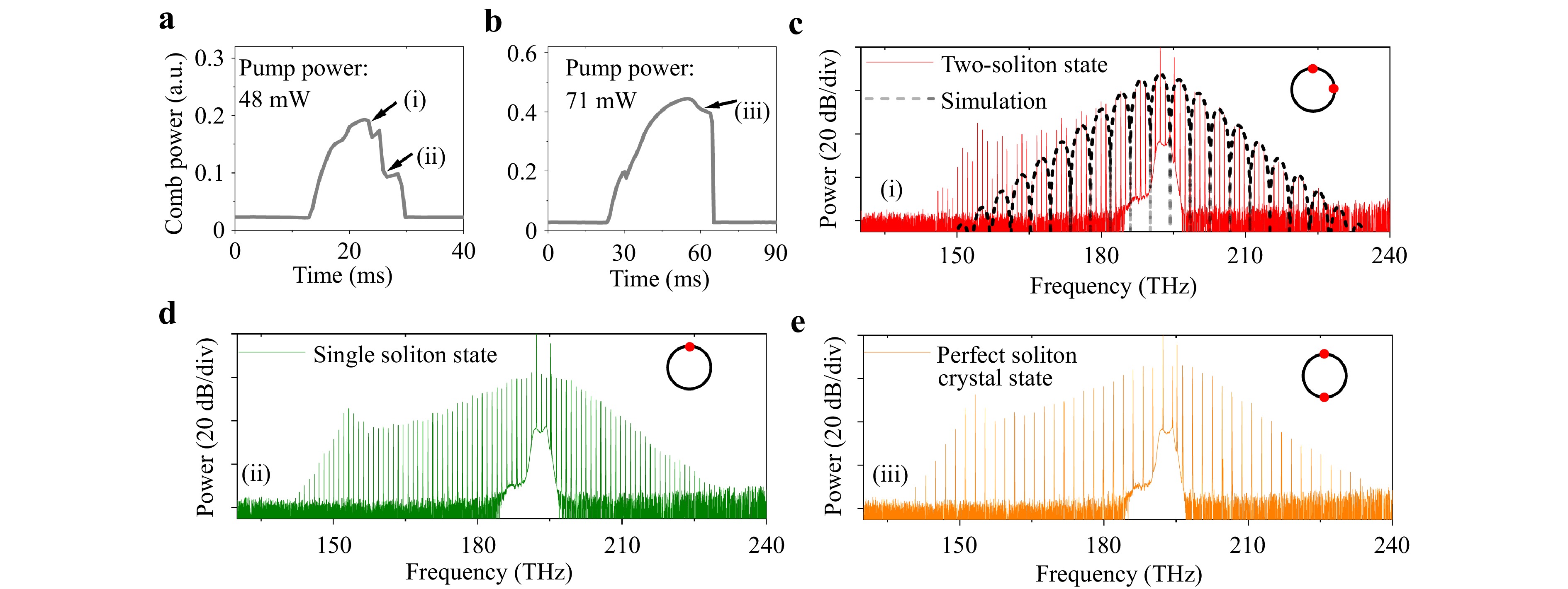
Fig. 7 Multi-soliton state and soliton crystal state in 1-THz SiCOI microring resonators. a, b Measured comb power as the pump frequency decreases. The coupled pump power is 48 mW a and 71 mW b. c-e Measured comb spectra corresponding to the recorded comb power in a and b. c The spectrum of the two-soliton state corresponds to the recorded comb power (i) in a. d The spectrum of the single-soliton state corresponds to the recorded comb power (ii) in a. e The spectrum of a perfect two-soliton state corresponds to the recorded comb power (iii) in b. The insets indicate the soliton number and the soliton position in the MRR.
$$ \begin{array}{l} {\rm{S^{(2)}}(\mu) = S^{(1)}(\mu) (2 + 2 \cos(\mu \psi))} \end{array} $$ (1) where $ {\rm{\psi}} $ is the relative azimuthal angle between the two solitons, $ {\rm{\mu}} $ is the comb mode index relative to the pump position, and $ {\rm{S^{(1)}}(\mu)} $ is the spectrum of a single-soliton with a sech-squared shape fitted from the experimental data. Fitting of the spectrum using Eq. (1) yields a relative azimuthal angle of 88$ ^{\circ} $, as shown in the inset of Fig. 7c for the two-soliton state. A further reduction in the pump frequency ultimately leads to a single soliton state (Fig. 7d).
In addition to multi-soliton formations, recent demonstrations have shown that $ {\rm{DKS}} $ also exhibits intriguing crystallisation processes73,74. These states are temporally ordered ensembles of soliton pulses around the perimeter of a microresonator called soliton crystals (SC). The formation of $ {\rm{DKS}} $ pulses in a crystal-like structure is related to avoided mode crossings. One special case among these states is the perfect soliton crystal state, characterised by evenly distributed $ {\rm{DKS}} $s on the resonator circumference, resulting in comb line spacing with multiple FSRs. At a pump power of 71 mW, we obtained a soliton spectrum with a repetition rate of two FSRs (Fig. 7e), with the comb power shown in Fig. 7b. SC formation relies on modulation of the intracavity pump field73, which can be achieved by AMX74 and delicate control of the pump condition75. In this study, modulation is introduced by the auxiliary laser through beating between the pump and control fields, which creates a periodic intracavity potential. This configuration provides a physically intuitive route for the SC formation and offers a practical degree of control over the resulting state76. Therefore, this scheme is feasible for synthesising different SC states and is an efficient approach for configuring the repetition rate of the comb.
-
Switching between the soliton states with different soliton numbers is governed by the thermal nonlinearity of the microresonator. In material platforms with positive thermo-optic (TO) coefficients, this process is typically accessible under unidirectional tuning conditions77. Moreover, the dissipative Kerr soliton (DKS) formation generally proceeds in a high-noise modulation instability (MI) regime. By contrast, recent demonstrations of lithium niobate (LN) microresonators have revealed a distinct soliton formation pathway, where self-starting DKS states can emerge without a pronounced MI regime78. This behaviour originated from the photorefractive effect in LN, which induced resonance blue shifts with increasing pump power. As a result, the photorefractive and Kerr-induced resonance shifts act in opposite directions, enabling soliton bursts and the bidirectional switching of soliton states22.
Similar phenomena were observed in the SiCOI MRR using the laser-cooling technique when the pump frequency was tuned forward and backward, as shown in Fig. 8a. The device has the same cross-sectional dimensions as those used in the previous subsection, with a similar Q factor of 1$ \times 10^6 $, but a smaller FSR of 360 GHz. The observed soliton burst dynamics originated from the interplay between the thermal nonlinearities induced by the pump and auxiliary lasers. Prior to pump tuning, the resonances were thermally redshifted using an auxiliary laser. When the pump enters resonance from the red-detuned side within the soliton existence range (i.e. while increasing the pump frequency), the increasing intracavity pump power further redshifts the resonance through both Kerr and thermal effects. Such a resonance shift increases the detuning between the resonance and auxiliary laser, thereby reducing the auxiliary intracavity power and weakening its thermal contribution, which induces a compensating blue shift in the resonance. This dynamic thermal balance stabilised the soliton state and enabled the soliton burst process. In our experiments, the burst process was consistently initiated from a three-soliton state and evolved toward higher soliton numbers with increasing pump frequency.
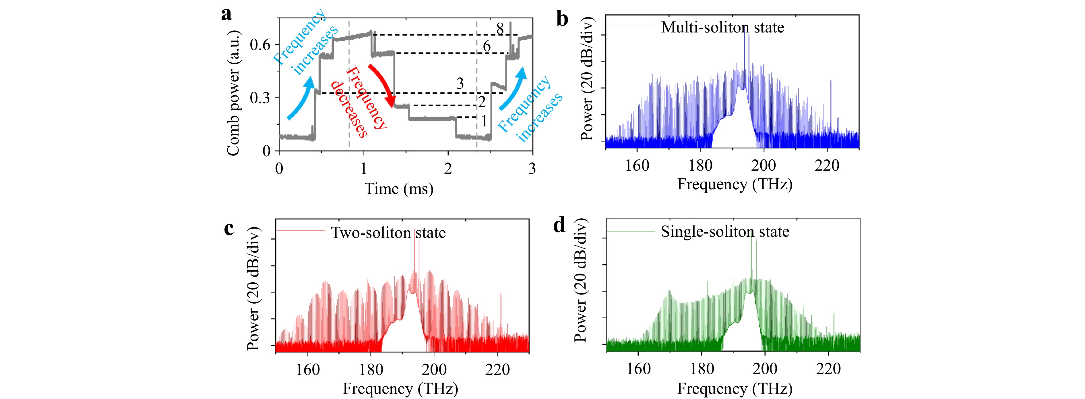
Fig. 8 Bi-directional switching of soliton states in a 360-GHz SiCOI MRR. a Measured comb power as a function of time when the laser frequency is scanned forward and backward across a few soliton steps. The dashed lines give the number of solitons. b Measured comb spectrum from a 360-GHz microring resonator with a multi-soliton state, c two-soliton state, and d single soliton state.
Another intriguing feature is the switching of soliton states during both pump-forward and pump-backward tuning, as shown in Fig. 8a. Using the laser-cooling technique, bidirectional switching becomes possible when the system enters the thermal overcompensation regime. Experimentally, this regime occurs when the variation in the $ Q $-power product of the pump laser (the product of the quality factor and the power coupled to the resonator) is weaker than that of the auxiliary laser, that is, $ |\Delta(Q_{{\mathrm{p}}}P_{{\mathrm{cp}}})| \lt |\Delta(Q_{{\mathrm{aux}}}P_{{\mathrm{caux}}})| $. In this regime, the thermal contribution from the auxiliary laser dominates the net thermo-optic response, thereby compensating for and potentially reversing the effective thermo-optic detuning evolution. This suppresses the thermal hysteresis and stabilises the pump within the soliton existence range during both forward and backward tuning. The observed behaviour agrees well with the bidirectional soliton switching reported for hydex microresonators79.
The experimental findings underscore that the laser cooling technique serves as an effective approach for enabling soliton bursts and bidirectional soliton switching, which are challenging to realise on material platforms with pronounced positive thermo-optic (TO) coefficients.
-
Most KCG studies have focused on microresonators with anomalous $ {\rm{GVD}} $ because it is a prerequisite for achieving phase-matching conditions for $ {\rm{OPO}} $. However, recent studies have also demonstrated KCG in normal $ {\rm{GVD}} $ microresonators11,80,81. It was found that KCG originated from $ {\rm{AMX}} $, which locally changes $ {\rm{GVD}} $. A common method for introducing $ {\rm{AMX}} $ involves employing a multimode waveguide in which transverse modes with the same polarisation interact with each other11,81. Other methods, such as polarisation-mode-interaction-assisted coupling, have also been theoretically investigated but have not yet been experimentally demonstrated82. Here, we observe that the coupling between transverse modes with orthogonal polarisations can also lead to KCG.
Fig. 9a shows the measured $ D_{\text{{int}}} $ of the characterised MRR with waveguide geometry displayed in the inset and a Q of 5$ \times 10^5 $, which fulfils the requirements of normal dispersion and strong AMXs. The SEM image of the MRR with a measured FSR of 106.31 GHz is shown in Fig. 9b. The $ {{D_2/2\text{π}}} $ is fitted as $ - $1.35 MHz. The dispersion was perturbed periodically at specific frequencies. The transmission spectra of $ {\rm{TE_{00}}} $ and $ {\rm{TM_{00}}} $ modes are shown in Fig. 9c, which illustrates that $ {\rm{AMX}} $ originates from intermodal coupling between $ {\rm{TE_{00}}} $ and $ {\rm{TM_{00}}} $ modes. The strong mode-splitting feature indicates hybridisation of the two modes when the resonant frequencies overlap at approximately 194.2 THz. In the comb generation experiments, we pumped the MRR at a power of 125 mW, tuned the laser to different resonances, and recorded the comb spectra (Fig. 9d). As shown in Fig. 9e, we pumped 8 different resonances from 194.33 to 195.07 THz and the comb spacing varies from 16 FSR to 9 FSR. Surprisingly, one of the first sidebands (the dashed line in Fig. 9d) is always anchored at the same frequency of approximately 196.02 THz, which is a sign of $ {\rm{AMX}} $-assisted comb generation83. The pinning of the first sideband to 196.02 THz was due to the largest resonance redshift at this position (0.62 GHz), indicating the strongest mode coupling. A further increase in pump power enables the generation of DPK combs80. However, the maximum coupled power of this sample is limited by its high coupling loss.
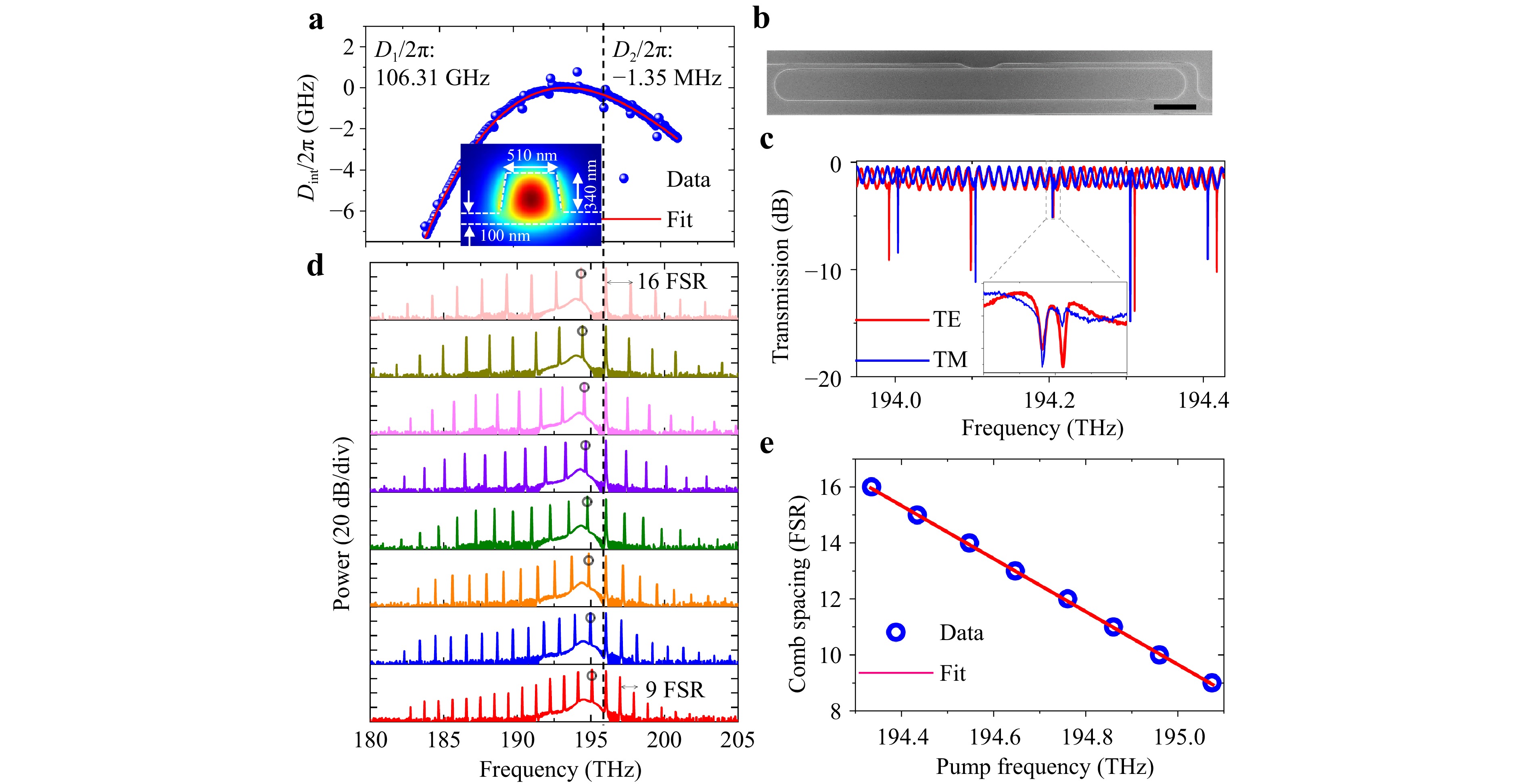
Fig. 9 KCG in $ {\rm{SiCOI}} $ $ {\rm{MRR}} $ with normal $ {\rm{GVD}} $. a Measured integrated dispersion with waveguide geometry shown in the inset. b $ {\rm{SEM}} $ image of a 106-GHz-$ {\rm{FSR}} $ microring resonator (scale bar: 40 µm). c Transmission spectrum of $ {\rm{TE_{00}}} $ and $ {\rm{TM_{00}}} $ modes. d Measured comb spectra at different pump frequencies with one of the first sidebands kept at around 196.02 THz. e Comb spacing as a function of the pump frequency.
-
In addition to the mode coupling between the transverse modes, $ {\rm{AMX}} $ can also be induced through the coupling between the clockwise ($ {\rm{CW}} $) and counterclockwise ($ {\rm{CCW}} $) propagating modes, resulting in lifted frequency degeneracy and mode splitting. These splittings are commonly observed in high-$ {{Q}} $ $ {\rm{MRR}} $s because of fabrication imperfections, such as sidewall roughness, which cause backward scattering of light. Alternatively, a more controllable approach involves the use of a photonic crystal (PhC) $ {\rm{MRR}} $, which allows for a frequency shift of the mode excited by the pump84.
Here, we investigate $ {\rm{DPK}} $ comb generation in normal $ {\rm{GVD}} $ $ {\rm{MRR}} $ with $ {\rm{CW}} $-$ {\rm{CCW}} $ mode coupling. The measured transmission spectrum for the 1,004-µm-long $ {\rm{MRR}} $ (Fig. 10a) with a waveguide geometry of 950 nm $ \times $ 340 nm exhibited an $ {\rm{FSR}} $ of 109.39 GHz and a $ {{D_2/2\text{π}}} $ of $ - $2.17 MHz, as confirmed by fitting the measured $ {{D_{{\mathrm{int}}}}} $ curve (Fig. 10b).
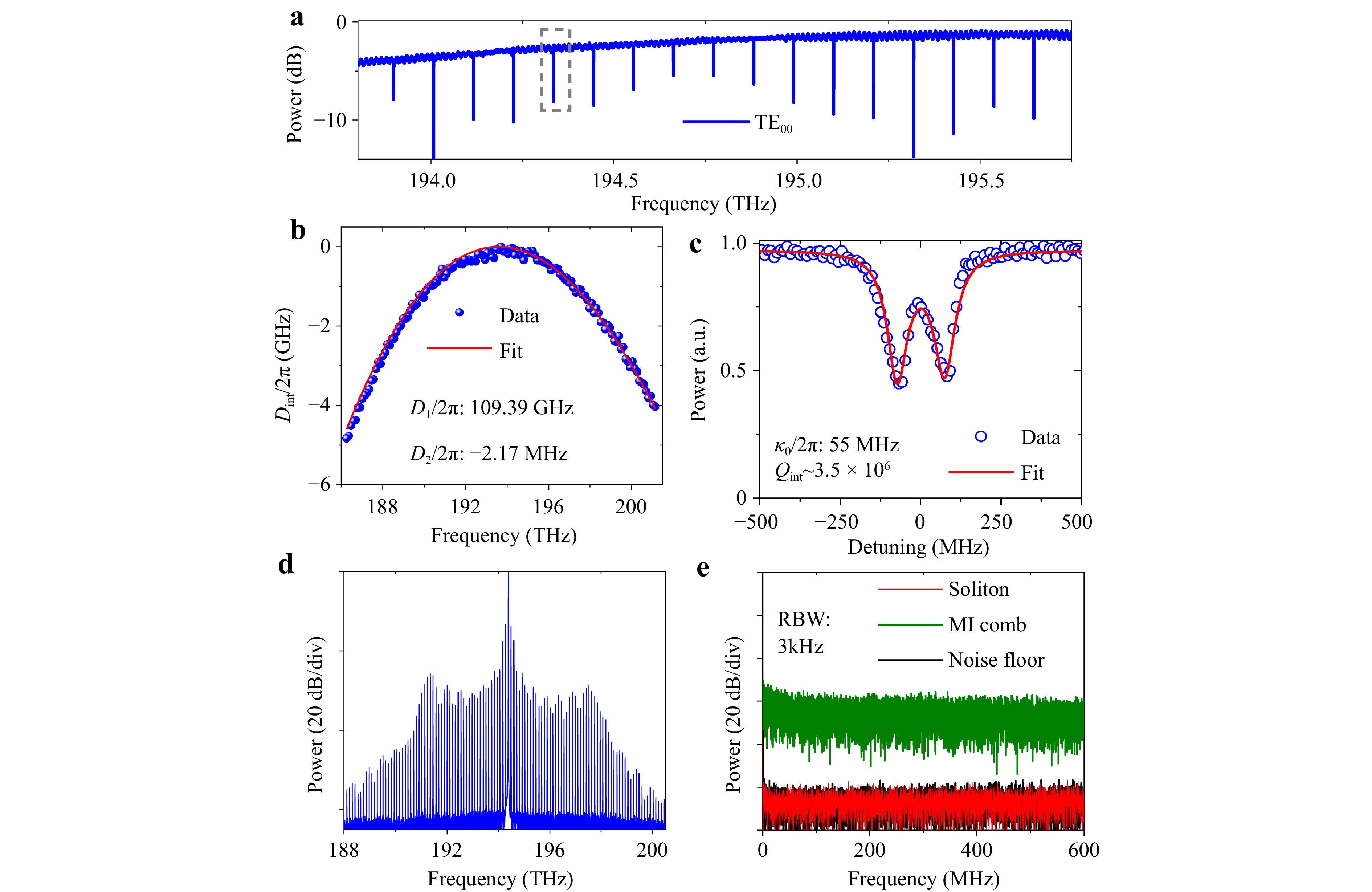
Fig. 10 Dark pulse Kerr comb in 109-GHz SiCOI MRR. a Transmission spectrum of the characterized MRR. b Measured integrated dispersion of the MRR. c Zoom in on the measured (normalized) transmission spectrum for the pump resonance in a. The optical spectrum d and the RF spectrum e of the 109-GHz DPK comb.
Normal-GVD conditions indicate that conventional Kerr comb generation is not expected in such MRRs. The clean transmission spectrum and dispersion curve verify that there is no coupling between the transverse modes, which could result in $ {\rm{AMX}} $. The magnified view of one of the resonances (Fig. 10c) reveals mode splitting at a rate of 151 MHz, which is sufficient to induce a resonance shift and enable $ {\rm{OPO}} $ and $ {\rm{DPK}} $ comb generation. This resonance was selected as the pump resonance for the subsequent $ {\rm{DPK}} $ comb generation experiments. During the $ {\rm{DPK}} $ comb generation experiment, the $ {\rm{CW}} $ laser was amplified and coupled in and out of the device through the lensed fibres. Tuning the laser to resonance from the blue side successfully generated a comb with a repetition rate of approximately 109 GHz (Fig. 10d). The spectral shape and low-noise radio frequency spectrum (Fig. 10e) confirm the realisation of $ {\rm{DPK}} $ comb. Importantly, $ {\rm{DPK}} $ was maintained in the same comb state for several hours without any feedback.
The successful generation of a $ {\rm{DPK}} $ comb in $ {\rm{SiCOI}} $ $ {\rm{MRR}} $ significantly enhances its practical use in ultrafast terahertz wireless communications85 because of its stability and higher pump-to-comb conversion efficiency compared with traditional soliton combs generated in anomalous microresonators.
-
In conclusion, we explored the fabrication, dispersion engineering, and dynamics of $ {\rm{SiCOI}} $ microresonators and elucidated their potential for $ {\rm{KCG}} $ and broadband soliton microcomb generation. By optimising the fabrication methods, we realised high-$ {{Q}} $ and high-confinement $ {\rm{SiC}} $ microresonators. By implementing a carefully designed dispersion and employing laser-cooling techniques, we successfully generated a broadband soliton microcomb. The laser cooling technique is an effective approach for mitigating thermal effects, offering versatile control of nonlinear states in $ {\rm{SiCOI}} $ microresonators. Furthermore, we demonstrated DPK comb generation in normal-dispersion microresonators. Taken together, these results establish SiCOI as a promising and versatile platform for integrated nonlinear photonics and chip-scale optical frequency comb systems.
These achievements bridge the long-standing fabrication gap that has limited 4H-SiC's transition from a theoretically promising material to an operational nonlinear photonic platform. The primary driver of this transition is the CMOS compatibility of the material, which offers a robust foundation for large-scale scalability and low-cost manufacturing. Table 2 provides a comprehensive comparison of the 4H-SiCOI platform with established Si-based materials across the key performance metrics. One of SiC's unique advantages is its simultaneously strong intrinsic $ \chi^{(2)} $ and $ \chi^{(3)} $ nonlinearities, which can support complex functionalities, such as monolithic self-referencing. This is further bolstered by the large optical damage threshold, which is essential for achieving high-power solitons and broad spectral bandwidths66. Although the Pockels effect in SiC is weaker than that in lithium niobate, it provides a pathway toward integrated modulators. Regarding the thermal properties, the higher thermo-optic coefficient of 4H-SiC poses challenges for broadband soliton generation using a single-pump scheme. Therefore, techniques such as fast pump wavelength sweeps, dual-mode pump schemes, and self-injection locking should be investigated to mitigate this problem.70,77,90 Moreover, SiC's exceptional thermal conductivity facilitates heat dissipation. To fully functionalize the SiCOI platform, it is necessary to integrate active components, such as lasers, high-performance modulators, and photodetectors. The readiness of SiCOI wafer-level manufacturing provides the potential for large-scale integration by incorporating technologies, such as heterogeneous integration91,92.
Property Si $ \mathbf{SiO_2} $ $ \mathbf{Si_3N_4} $ 4H-SiC Refractive index 3.47 1.45 1.98 2.58 Bandgap (eV) 1.1 8.9 5.0 3.2 Transparent window ($ \mu $m) 1.2–8 0.2–4 0.4–4.6 0.37–5.6 Nonlinear index ($ \rm m^2 W^{-1} $) $ 5\times 10^{-18} $ $ 3\times 10^{-20} $ $ 2.5\times 10^{-19} $ $ (2-9)\times 10^{-19} $ Intrinsic $ \chi^{(2)} $ nonlinearity (pm/V) – – – 6.5–12.5 (@ 1.064 $ \mu $m) Electro-optic effect Free-carrier plasma dispersion – – Pockels effect (0.01–0.7 pm/V) Thermo-optic coefficient @ 300 K ($ {\mathrm{K}}^{-1} $) $ \rm 1.8\times 10^{-4} $ $ 8\times 10^{-6} $ $ \rm 2.5\times 10^{-5} $ $ \rm 3.75\times 10^{-5} $ Thermal conductivity ($ \rm Wm^{-1}K^{-1} $) 130–150 1.1–1.4 25–36 360–490 Achieved Q factor $ 1.2 \times10^{9 \ *} $86 $ 8.7 \times 10^{8 \ *} $87 $ 7.2 \times 10^{8\ **} $88 $ 9 \times10^{6} $89 Table 2. Comparison of key properties between different silicon-based material platforms. All parameters are at 1.55 $ \mu $m unless otherwise specified. $ ^* $Whispering gallery mode.$ ^{**} $ Weak confinement in Si3N4 waveguide.
This also opens new avenues for emerging applications. For example, 4H-SiC is of particular interest in quantum photonics. The inherent capability of 4H-SiC to host stable, high-performance colour centers (such as silicon vacancies and divacancies) allows the monolithic integration of single-photon emitters with the now-proven high-$ Q $ nonlinear resonators, facilitating enhanced light-matter interactions for quantum information processing35,61. Furthermore, the exceptionally wide transparency window of 4H-SiC (0.37–5.6 $ \mu $m) positions the SiCOI platform as a superior candidate for molecular spectroscopy and environmental sensing, reaching mid-IR spectral regimes where silicon nitride becomes opaque.
By successfully bridging the gap between high-precision manufacturing and functional nonlinear systems, this study establishes the 4H-SiCOI platform as a scalable, high-performance foundation for the next generation of integrated nonlinear and quantum photonic technologies.
-
This work was supported by the European Research Council under the EU's Horizon 2020 research and innovation program (grant agreement no. 853522, REFOCUS), Independent Research Fund Denmark (ifGREEN 3164-00307B), and the Danish National Research Foundation (SPOC ref. DNRF123), Innovationsfonden (Green-COM 2079-00040B), National Key R&D Program of China (grant No. 2022YFA1404601, No. 2022YFA1404602), Chinese Academy of Sciences Project for Young Scientists in Basic Research (grant No. YSBR-69), and National Natural Science Foundation of China (grant Nos. 62293521, 12575313, 12074400, and 62205363).
4H-silicon carbide integrated platform: from manufacturing to nonlinear photonics
- Light: Advanced Manufacturing , Article number: 114 (2026)
- Received: 16 January 2026
- Revised: 29 June 2026
- Accepted: 01 July 2026 Published online: 10 November 2026
doi: https://doi.org/10.37188/lam.2026.114
Abstract: Silicon carbide (SiC) has emerged as a promising integrated platform for quantum and nonlinear photonics owing to its unique combination of a wide bandgap, large Kerr nonlinearity, excellent thermal conductivity, and compatibility with silicon photonics. While progress in fabrication has enabled high-confinement microresonators, achieving industrial-grade, low-loss devices requires overcoming significant manufacturing hurdles related to material defects and surface roughness. This paper provides a comprehensive investigation of advanced manufacturing protocols for wafer-scale (4-inch) 4H-silicon carbide-on-insulator (SiCOI) integrated platforms. This study systematically compares two primary fabrication routes, ion-cut method and bulk wafer thinning, and investigates their impact on material crystal quality and optical loss performance. Using an optimised manufacturing process, we achieved sub-nanometre sidewall roughness and intrinsic quality factors ($Q$) of up to 5.8 million. Furthermore, we provide an overview of our recent progress in Kerr-comb generation using these high-confinement microresonators, including the realisation of sub-milliwatt-threshold Kerr combs, single solitons, and broadband octave-spanning states. We also investigate complex soliton dynamics, including soliton crystals and bidirectional switching. This study establishes a robust manufacturing foundation for the SiCOI platform, bridging the gap between high-precision fabrication and functional chip-scale nonlinear optical systems.
Research Summary
Integrated photonics: Silicon carbide chips generate broadband light combs
A refined manufacturing process turns silicon carbide into ultra-low-loss optical chips that convert a single laser beam into broad ‘combs’ of evenly spaced light frequencies, with uses from telecommunications to quantum technology. Silicon carbide is appealing for chip-based optics because it transmits light over a wide range, conducts heat well and suits standard semiconductor fabrication, but defects and surface roughness have limited its performance. Minhao Pu at the Technical University of Denmark, Xin Ou at the Shanghai Institute of Microsystem and Information Technology, and co-workers compared two wafer-scale fabrication routes and refined a surface-smoothing step to reach very low optical loss. Their ring resonators turned continuous laser light into broadband frequency combs and stable soliton pulses at low power. The work positions silicon carbide as a versatile platform for nonlinear and quantum photonic chips.
Rights and permissions
Open Access This article is licensed under a Creative Commons Attribution 4.0 International License, which permits use, sharing, adaptation, distribution and reproduction in any medium or format, as long as you give appropriate credit to the original author(s) and the source, provide a link to the Creative Commons license, and indicate if changes were made. The images or other third party material in this article are included in the article′s Creative Commons license, unless indicated otherwise in a credit line to the material. If material is not included in the article′s Creative Commons license and your intended use is not permitted by statutory regulation or exceeds the permitted use, you will need to obtain permission directly from the copyright holder. To view a copy of this license, visit http://creativecommons.org/licenses/by/4.0/.

 DownLoad: