




-
Ultrafast lasers have steadily expanded the scope of optical manufacturing, from photonic structures in crystals to sub-20-nm surface nanowriting and the stealth dicing of hard wafers. In recent years, the lateral resolution of optical manufacturing has improved significantly through near-field, high-numerical aperture (NA) lenses and super-resolution schemes, thereby enabling advanced surface structuring, additive fabrication, and localised subsurface writing1–13, as summarised in Table 1. However, such enhancement cannot directly translate to a small kerf when slicing crystals or transparent solids owing to the limited depth of field of a Gaussian beam. Although utilising Bessel beams may significantly extend the field depth, the resulting kerf widths measure hundreds of nanometres with rough surfaces14. This is not merely an engineering inconvenience. For high-value transparent materials such as laser crystals and semiconductor substrates, every additional micrometre of kerf translates into wasted feedstock, thicker polishing allowances, and higher costs. This bottleneck remains a longstanding problem in laser manufacturing.
Processing technique Material Characteristic advance Three-dimensional (3D) femtosecond laser writing1 Yttrium aluminium garnet (YAG) and sapphire 3D nanostructures with ~100 nm feature sizes Femtosecond projection two-photon lithography2 Photoresist Nanowires with lateral widths of 130–140 nm and axial heights down to 175 nm Optical far-field-induced near-field breakdown3 TiO2 films Surface nanowriting with spatial resolution < 20 nm Picosecond laser-induced micro-explosion4 4H-SiC Picosecond slicing with cutting width < 2 μm and 250 μm thick wafers Longitudinal laser-field material processing5 Sapphire, Si, and Cu surfaces 10–30-nm features with an aspect ratio > 16 in the far field Kinetically regulated material assembly6 Metals, two-dimensional (2D) materials, oxides, and diamond 3D nanostructures with 20–200-nm resolution Photoexcitation-induced chemical bonding7 Semiconductor quantum dots 3D nanoprinting with a minimum lateral linewidth of 81 ± 4 nm Picosecond laser stealth dicing8 4H-SiC Stealth dicing with a chipping width < 3 μm and section roughness < 500 nm Super-stealth dicing9 Transparent solids including fused silica, LiTaO3, LiNbO3, YAG, Ce:YAG, and β-Ga2O3 Nanometric-precision dicing with cutting widths measuring tens of nanometres and aspect ratios of 1,000–10,000 3D nonlinear laser nanolithography10 Silicon Embedded nanostructures with feature sizes down to 100 ± 20 nm deep inside silicon Laser-induced periodic surface structures11 2D NbOI2 Groove widths down to ~14.5 nm (~λ/73) fabricated in ambient air Wet chemical etching-assisted aberration-enhanced single-pulsed femtosecond laser-supplemented nanolithography12 Crystals, glasses, and Si-based semiconductors 25-nm features, aspect ratios > 104:1, and 10 mm2 holey nanostructures Interferometric scattering-based optical tomoslicing13 Fused silica, YAG, and MgAl2O4 7-nm kerf, mass loss < 1%, 30 × 10 mm slicing, and theoretical industrial efficiency up to 400 mm²/s Table 1. Representative recent advances in optical manufacturing in terms of feature resolution and depth-to-width aspect ratio.
Instead of pursuing conventional approaches such as optimising NAs or focusing techniques, Chai et al. transformed the physical role of scattering4,5,8,9,13. In most laser-processing scenarios, scattering is a detrimental mechanism, which perturbs focusing, redistributes energy, and degrades precision. Chai et al. inverted this logic. They intentionally created an initial nanopore via femtosecond-laser-induced micro-explosion and then used the nanopore as a seed scatterer. When the incident beam was laterally offset from the seed within a critical distance (approximately 200 nm in fused silica; Fig. 1b–d), the scattered field interfered with the undisturbed portion of the beam, thus yielding a sufficiently strong localised intensity maximum to generate a secondary nanopore. The secondary pore became the next scatterer, and the process was repeated in a controlled cascade. In other words, the structure being written participated in writing the next structure. This interferometric-scattering mechanism achieves energy localisation independent of the original focal ellipsoid. By adjusting the pulse offset, the authors steered the trajectory and orientation of sequential nanopores. Moreover, by shifting from a point focus to a line field generated using a cylindrical lens (Fig. 1f), they translated the same principle into interferometric scattering-based optical tomoslicing (i-SOT), which is a plane-slicing strategy instead of a conventional crack-guided separation process. This strategy offers high throughput (1 m/s) and scalability, and the resulting surface simultaneously offers superior quality (Ra = 9 nm)13.
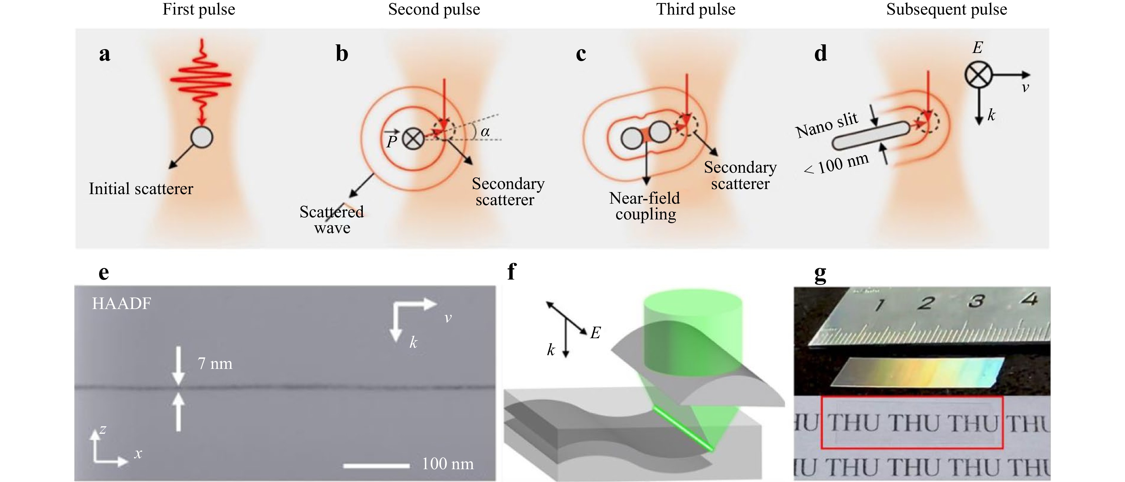
Fig. 1 Interferometric scattering as the basis of interferometric scattering-based optical tomoslicing (i-SOT). a–d Schematic of scatterer generation and propagation. e High-angle annular dark-field scanning transmission electron microscopy image of a horizontal nano-slit showing the 7-nm raw kerf. f Schematic of line-field generation using a cylindrical lens. g Planar wafering with high transmittance by cold splitting without etching. The wafer measures 30 × 10 mm (Images adapted from Ref. 13).
The performance metrics explain the importance of this concept. Additionally, the experiments were conducted with a modest NA of 0.6, thus avoiding the requirement for extremely high-NA optics. In fused silica, i-SOT yielded raw kerf widths down to 7 nm (Fig. 1e). Furthermore, the method accommodates geometries rarely attainable via conventional wafering, including multilayer slicing, 45° tilted planes, and wavy cross-sections. In addition to fused silica, Chai et al. applied i-SOT to crystalline yttrium aluminium garnet (YAG) and MgAl2O4, thus yielding ultrathin wafers that were approximately 8.6–9.5-μm thick and demonstrating that the sliced YAG plates retain notable mechanical integrity. i-SOT employs a line field instead of point-by-point raster scanning, thereby offering high throughput and precision. A 30 × 10 mm transparent slice can be created directly (Fig. 1g), and the authors predict that by adopting industrial-class femtosecond sources, the theoretical slicing efficiency may reach 400 mm2/s. Most importantly, combining ultrathin wafering with nanometric kerfs reduces mass loss from approximately 30% to below 1%, thus bringing laser wafering close to an almost-ideal, “kerf-free” manufacturing process13.
Perhaps the most profound impact of this study is conceptual. Over the past two decades, researchers have progressively leveraged principles from super-resolution optical imaging, nonlinear thresholding, and near-field confinement to enhance fabrication resolution. Chai et al. provided a different perspective: the medium can be actively engineered to serve as an interferometric contributor to the manufacturing process. Once scattering is seeded, directed, and cascaded, this process ceases to exert a parasitic effect and becomes a tool for energy localisation. This reversal is elegant yet practical and represents a family of laser-manufacturing strategies where sub-diffraction precision, high throughput, and low material loss are pursued simultaneously instead of through mutual compromise. For transparent solids, light scattering may have just changed from a nuisance into the blade itself 3,5,9,13.
Transforming scattering into a seed of a nanometric blade
- Light: Advanced Manufacturing , Article number: 122 (2026)
- Received: 24 June 2026
- Revised: 15 July 2026
- Accepted: 16 July 2026 Published online: 10 October 2026
doi: https://doi.org/10.37188/lam.2026.122
Abstract: Chai et al. converted interferometric scattering from a persistent optical limitation into an effective tomoslicing technique, which delivers an unprecedented 7-nm kerf width and almost lossless wafering. Furthermore, this method is a robust and scalable approach for the low-waste manufacturing of transparent crystals and semiconductor substrates.
Rights and permissions
Open Access This article is licensed under a Creative Commons Attribution 4.0 International License, which permits use, sharing, adaptation, distribution and reproduction in any medium or format, as long as you give appropriate credit to the original author(s) and the source, provide a link to the Creative Commons license, and indicate if changes were made. The images or other third party material in this article are included in the article′s Creative Commons license, unless indicated otherwise in a credit line to the material. If material is not included in the article′s Creative Commons license and your intended use is not permitted by statutory regulation or exceeds the permitted use, you will need to obtain permission directly from the copyright holder. To view a copy of this license, visit http://creativecommons.org/licenses/by/4.0/.

 DownLoad: