


-
In recent years, various approaches have been followed for the realisation of solid-state single-photon emitters1,2. Single-photon emission from semiconductor quantum dots (QDs) has been shown to be a pure and efficient non-classical light source with a high degree of indistinguishability, so that they could become an essential tool for future quantum communication3-9. To create secure, wide-spread quantum communication networks10-12, high-brightness single-photon sources are necessary. In the case of QDs, the total internal reflection (TIR) as a result of the high semiconductor-to-air refractive index contrast severely limits the single-photon extraction efficiency. Therefore, many attempts have been made to increase the extraction efficiency of quantum dots, including photonic crystal structures13, cavity quantum electrodynamics5,6,14-16, plasmonic surface effects17, and solid immersion lenses (SILs)18-22. Another crucial step in the development of practical quantum networks is the implementation of quantum repeater protocols, which enable long-distance quantum communication via optical fibre channels. These protocols rely on the use of highly indistinguishable, entangled photons5,23-25, which require the use of single-mode fibres26-28. Thus, an efficient on-chip single-mode fibre-coupled quantum light source is a key element in the realisation of a QD-based real-world quantum communication network.
In this paper, we first focus on enhancing the extraction efficiency of semiconductor QDs by optimising micrometre-sized SIL designs. Two state-of-the-art technologies, i.e., low-temperature deterministic lithography21,29 and femtosecond 3D direct laser writing30-39, are used in combination to deterministically fabricate micro-lenses on pre-selected QDs. Because of the high flexibility of 3D direct laser writing40, various SIL designs, including hemispherical SILs (h-SILs), Weierstrass SILs (W-SILs), and total internal reflection SILs (TIR-SILs), can be produced and compared with respect to single-photon extraction enhancement. The experimentally obtained values are compared with analytical calculations, and the role of misalignment between SIL and QD as an error source is discussed in detail. We then highlight the implementation of an integrated single-mode fibre-coupled single-photon source based on 3D printed micro-optics41. A 3D printed fibre chuck is used to precisely position an optical fibre onto a QD with a micro-lens printed on top. This fibre is equipped with another specifically designed 3D printed in-coupling lens to efficiently guide light from the TIR-SIL into the fibre core. Finally, we demonstrate that our compact on-chip solution is capable of producing an in-coupling efficiency of 26 ± 5% into a single-mode fibre.
-
To estimate the photoluminescence (PL) intensity enhancement after the printing of an h-SIL, calculations were performed based on previous works18,42. Here, the QD was assumed to have a dipole emission characteristic, the intensity of which can be described as
$$ \begin{array}{r}I\left({\theta }_{1},\phi \right)\propto \dfrac{3}{8\pi }\left[1-{\rm{sin}}^{2}\left({\theta }_{1}\right){\rm{cos}}^{2}\left(\phi \right)\right]\end{array} $$ (1) using spherical coordinates. The collection efficiency for a certain detector collection numerical aperture (NA) can be calculated by integration over the full upper half solid angle:
$$ \begin{array}{r}\eta ={\displaystyle\int }_{0}^{{\theta }_{{\rm{max}}}}{\rm{d}}{\theta }_{1}{\displaystyle\int }_{0}^{2\pi }{\rm{d}}\phi \hspace{0.25em}I\left({\theta }_{1},\phi \right)\end{array} $$ (2) $ {\theta }_{{\rm{max}}} $ accounts for the total internal reflection (TIR) condition at the gallium arsenide (GaAs) to-air/lens interface and can be expressed as$$ \theta _{{\rm{max}}}^{{{\rm{no}}}\;{\rm{SIL}}} = {\rm{arcsin}}\left( {\frac{{{n_{{\rm{air}}}}}}{{{n_{{\rm{GaAs}}}}}} \cdot NA} \right)$$ (3) $$ \theta _{{\rm{max}}}^{{\rm{h - SIL}}} = {\rm{arcsin}}\left( {\frac{{{n_{{\rm{SIL}}}}}}{{{n_{{\rm{GaAs}}}}}} \cdot NA} \right) $$ (4) for structures without SIL and with a hemispheric SIL (h-SIL), respectively. The numerical integration of Eq. 1 over the full upper half solid angle, while considering the conditions for
$ {\theta }_{{\rm{max}}} $ , results in the solid collection efficiency curves displayed in Fig. 1a. From these curves, a detector collection NA-independent enhancement of$ {\tilde \eta _{{\rm{ideal}}}} = 2.28$ is derived by division of the upper solid curve by the lower solid one. This is shown in Fig. 1b as a solid blue curve. However, reflections at the interfaces are not yet taken into account. This is performed by multiplying Eq. 1 with the transmission Fresnel formula for each occurring refraction. Because the polarisation of the emitted light is mostly unpolarised, a transmission of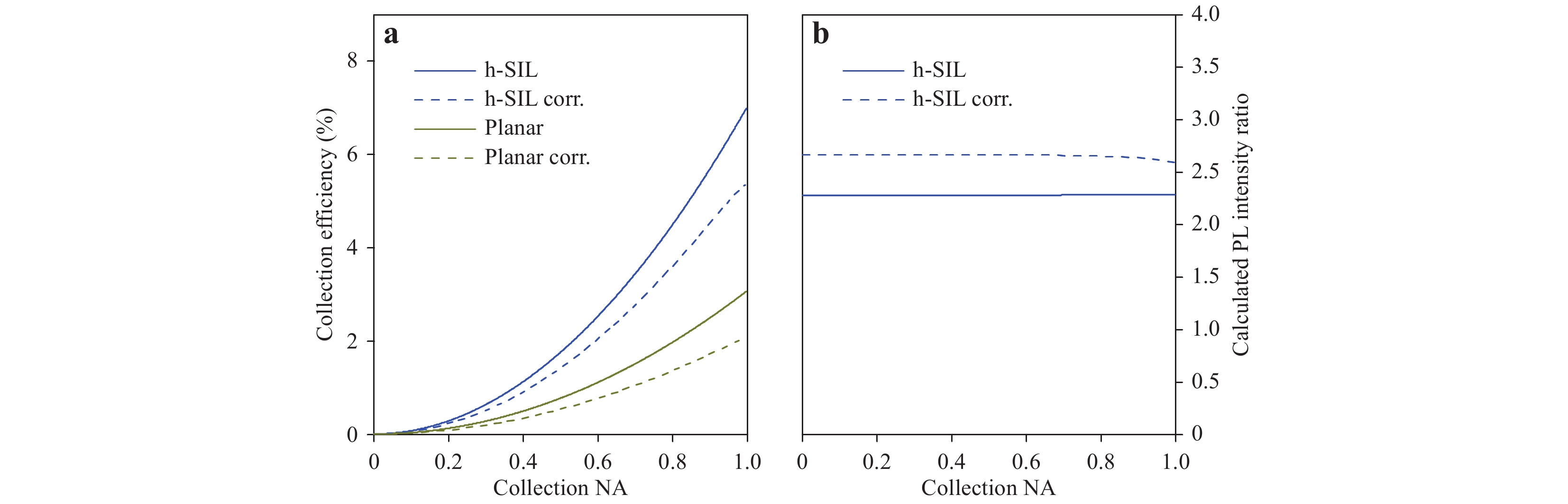
Fig. 1
a Calculated collection efficiencies for planar extraction and extraction with an h-SIL made from IP-Dip photoresist ($ n=1.51 $ $ {n}_{\rm{GaAs}}=3.5 $ $ {n}_{\rm{SIL}}=1.51 $ $ {n}_{\rm{air}}=1.0 $ $$ \begin{array}{r}{T}_{\rm{total}}=\dfrac{{T}_{s}+{T}_{p}}{2}\end{array} $$ (5) can be estimated for each interface.
$ {T}_{s} $ and$ {T}_{p} $ represent the perpendicular and parallel polarised transmissions with respect to the interface. Thus, a reflection-corrected intensity enhancement of$ {\tilde \eta _{{\rm{corr}}}} \approx 2.65$ (constant under NA variation) is calculated, accounting for one reflection at each interface (see the dashed blue curve in Fig. 1b). All calculations are based on the refractive indices$ {n_{{\rm{GaAs}}}} = 3.5$ ,$ {n_{{\rm{SIL}}}} = 1.51$ , and$ {n_{{\rm{air}}}} = 1.0$ .For the sample processed here, markers are transferred to the substrate after resist development via inductively coupled plasma reactive ion etching (ICP-RIE). The accurate placement of the alignment markers with respect to the pre-selected QD can be seen via a micro-photoluminescence (µ-PL) scan after marker fabrication, as shown in Fig. 2a. For the data displayed in this figure, a high-resolution µ-PL map is merged with the simultaneously acquired reflectivity map provided by an excitation laser scan. Fig. 2b shows a top-view microscope picture of a deterministically printed lens with a diameter of 20 µm, which is centred with high accuracy on the QD. A quantitative study of this placement accuracy is discussed later in this work. For this sample, both deterministic lithography and characterisation are carried out in a deterministic low-temperature lithography setup. A schematic of the measurement principle is shown in Fig. 2c. The QD is excited by a laser at
$ \lambda =658\;{\rm{ nm}} $ . Light emitted by the QD underneath the lens is collected by a$ 100\times $ low-temperature microscope objective ($ {\rm{NA}}=0.8 $ ) and passes through the dichroic beam splitter (long pass 675 nm), while the reflection of the red laser is reflected back into the excitation fibre.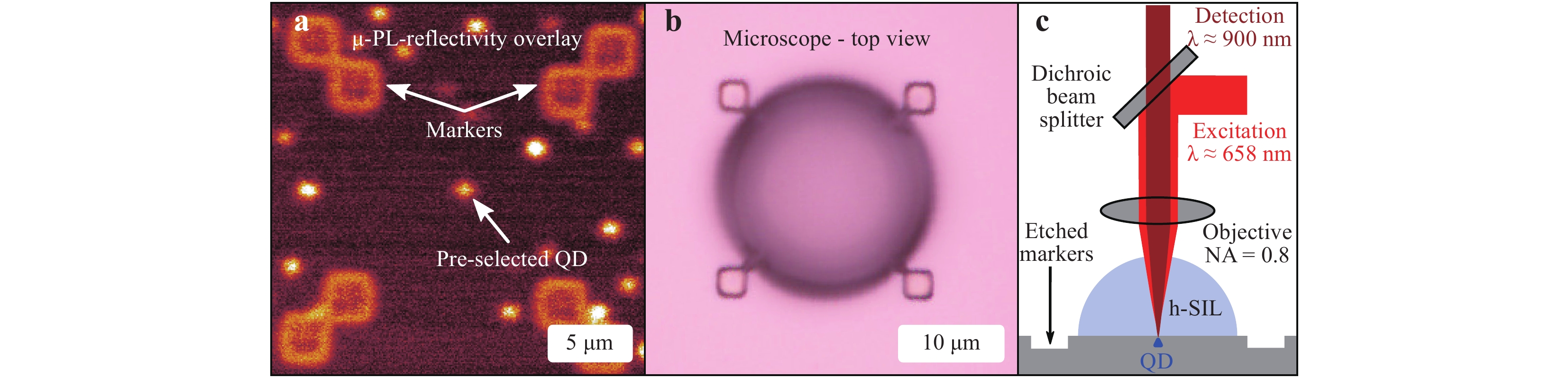
Fig. 2
a High-resolution overlay of a µ-PL map and the corresponding reflectivity map (200 × 200 pixels) after etching of the deterministically placed markers. The pre-selected QD appears to be well located in the centre of the alignment structures. A longpass filter with a cut-off wavelength at 865 nm was used to suppress the wetting layer signal. b Microscope top view of a deterministically 3D printed h-SIL with a diameter of 20 µm aligned on the etched markers. c Simplified sketch of the µ-PL setup. A laser diode emitting at 658 nm is used for QD excitation. The emitted light is transmitted via a dichroic beam splitter and coupled into a single-mode fibre, which sends the photons to a spectrometer equipped with a CCD camera and a photon counting module. Figure reproduced from Ref. 21.In general, h-SILs are known to provide a better focus of the laser beam43-45. Because of the smaller spot size on the sample, a better signal-to-noise-ratio is observable when acquiring a µ-PL intensity map. Fig. 3a and b show a high-resolution µ-PL map of the same single QD before and after the placement of an h-SIL. A long-pass filter with a cut-off wavelength of 865 nm was used to suppress the wetting layer contribution. To obtain the QD position with respect to the system coordinates, a 2D Gaussian surface fit was applied to the high-resolution maps in Fig. 3a and b. The error in the determination of the position of the maximum intensity is called the localisation accuracy. By placing an h-SIL, an improvement in the horizontal scan direction from 1.6 nm to 800 pm and in the vertical direction from approximately 1.1 nm to 660 pm could be observed. In summary, h-SIL placement improves localisation accuracy by a factor of approximately 2. It is worth mentioning that the QD localisation only refers to the system coordinates, not to any processed markers or structure. Using the system specifications, an upper bound of the placement accuracy can be estimated with a conservative value of ± 50 nm, which is negligible in comparison with the printed h-SIL size (diameter of 20 µm). Because the h-SIL reduces the spot size by a factor of
$ 1/{n}_{\rm{SIL}} $ 45 (here,$ {n}_{\rm{SIL}}\approx 1.51 $ ) and provides a magnified image of objects underneath it at the same time by a factor of$ {n}_{\rm{SIL}} $ , the FWHM should be mostly invariant, whether an h-SIL is present or not. This is verified by determining the FWHM in the extracted cross-sections in Fig. 3c and d. The respective values for the QD shown here are$ {\rm{FWHM}} = 1322 \pm 46\;{\rm{nm}} $ and$\rm FWH{M_{h - SIL}} = 1149 \pm 12\;{\rm{nm}} $ .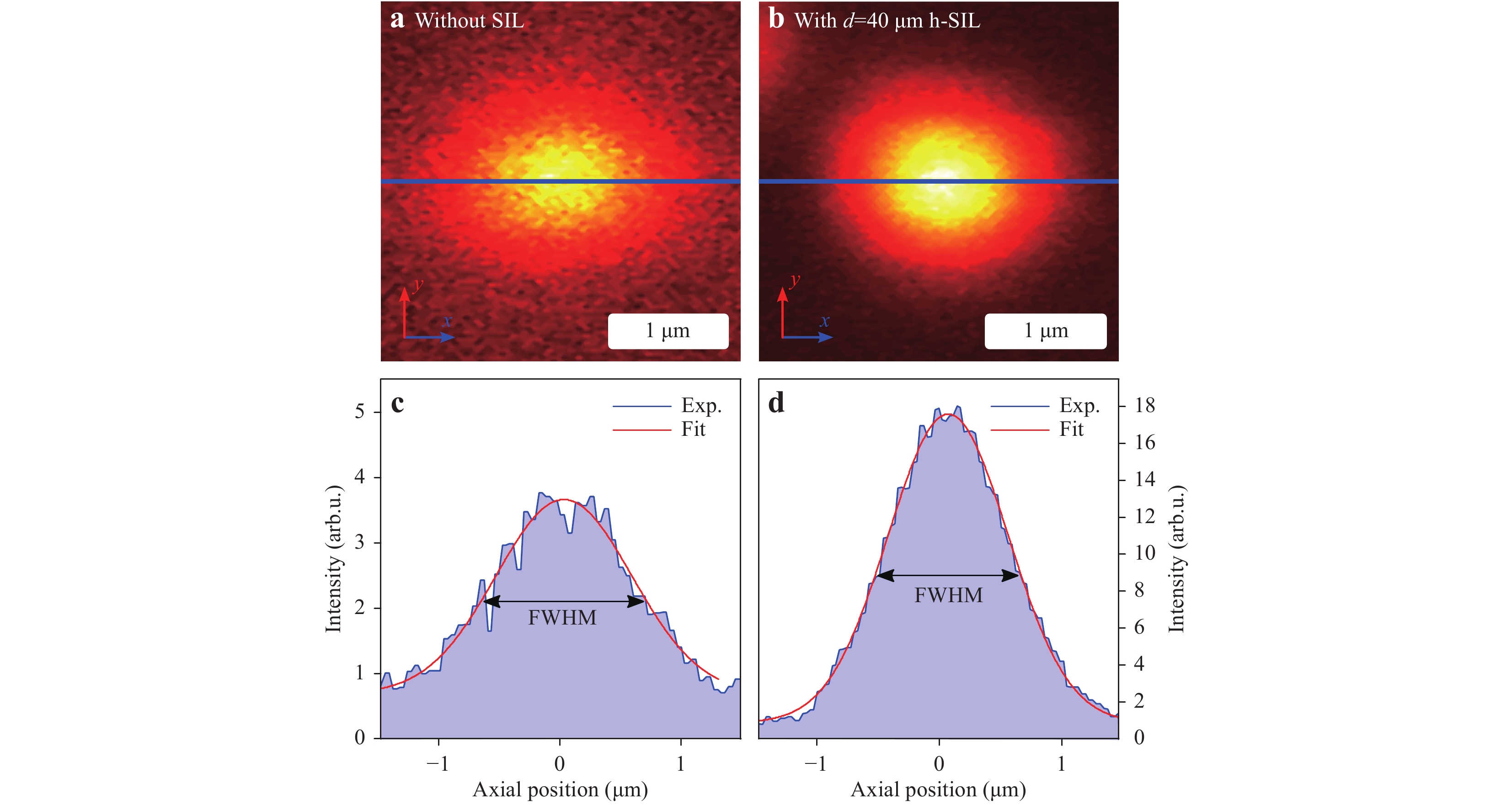
Fig. 3
a and b High-resolution µ-PL maps of the same isolated QD without the h-SIL and after fabrication, respectively. A longpass filter with a cut-off wavelength of 865 nm was used to suppress the contribution of the wetting layer. c and d Extracted intensity profiles (blue) of the maps from a and b (blue line) and corresponding Gaussian fits (red). A Gaussian fit is used for the signal as a convolution of the Gaussian laser beam and the QD spectrum. Figure analogous to Ref. 21.One question that remains is how precisely the 3D printer can be aligned on the etched markers. To address this question, the laser reflection pattern on top of the h-SIL was imaged on the built-in camera module, which appears circularly symmetric when aligned on the lens centre. Furthermore, the distance to the maximum PL signal was recorded, which provides the measured displacement values in Tab. 1. However, these values do not represent the real lens displacement because they do not account for refraction at the interfaces. To determine the refraction-corrected
$ \varDelta {x}_{0} $ values in the last column in Tab. 1, ray optics calculations were performed, as illustrated in Fig. 4. Fig. 4a shows the ray optics calculations for a non-displaced lens. The blue lines represent the fraction of light collected by the used detector collection NA. For a displacement of 0 nm, the central ray (here depicted in green) coincides with the ray that leaves the GaAs and the h-SIL orthogonally. However, if the QD is displaced with respect to the lens centre by$ \varDelta {x}_{0} $ , the maximum PL signal is measured at a site that does not correspond to the real QD position, but rather to the position of the depicted green ray in Fig. 4b. The obtained optimised coordinates now serve as a raw displacement input for further ray optics calculations that consider refraction at the interfaces. The values obtained with this method are reported for various SIL diameters in Tab. 1. These values demonstrate that sub-micrometric SIL placement accuracy, approximately 590 nm on average, could be achieved with the fabrication method utilised in this section. Because the laser used in the 3D printing phase is diffracted at the etched marker edges, it may be beneficial to switch to the deposition of metal markers to further improve these values. In the following paragraphs, this placement accuracy is shown to be improved by the use of metal markers, even in combination with lens geometries more sensitive to spatial displacement. Employing a similar approach to Fig. 4, the PL signal was already at its maximum when the beam was focused at the lens centre, demonstrating a higher placement accuracy than the one achieved for h-SILs.SIL diameter (μm) Measured displacement (nm) Refraction-corrected displacement $ {{\varDelta }}{{x}}_{{{0}}} $ (nm) 20 1350 850 30 510 400 30 900 650 40 860 460 40 1210 680 50 330 220 50 1350 730 75 1270 740 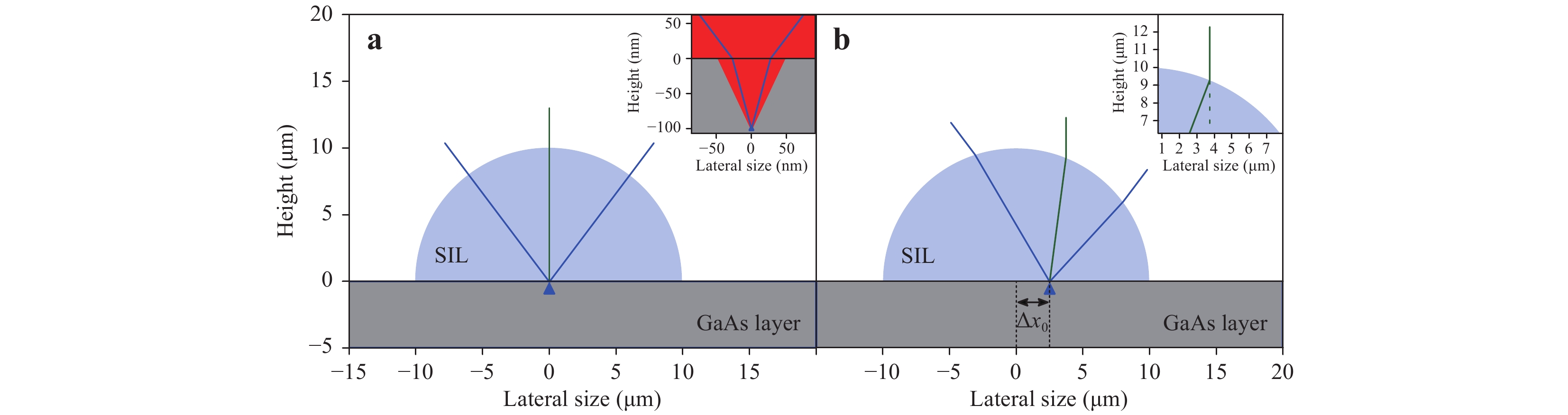
Fig. 4 Illustration of the ray optics calculations to determine the displacement of the SIL.
a The lens is perfectly centred with respect to the QD position. b The lens and the QD exhibit a lateral displacement of$ \varDelta {x}_{0} $ Changing the refractive index on top of the sample surface from
$ n=1 $ for the SIL material to$ n\approx 1.51 $ leads to a change in the condition of TIR. The critical angle increased from 16.6° to 25.6°, resulting in an increase in light extraction. Indeed, the direct spectral comparison in Fig. 5 before and after the h-SIL fabrication shows a broadband emission enhancement of all lines. This is observable in combination with an overall shift to higher emission energies.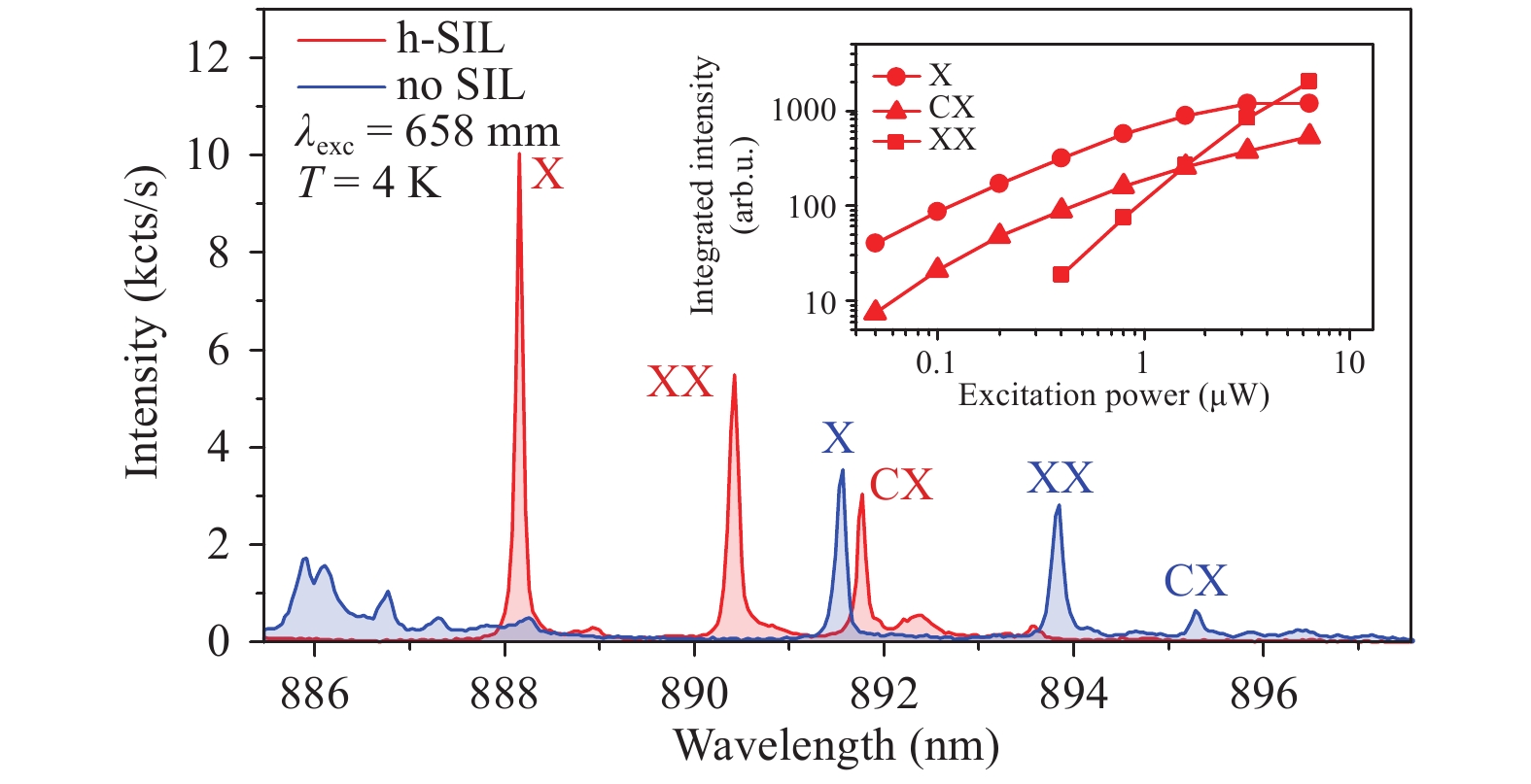
Fig. 5 Exemplary spectrum of a QD without the lens before fabrication (blue) and with the lens after deterministic lithography and 3D printing (red).
The inset shows a power-dependent measurement of the QD emission lines after lens fabrication. Exciton (X) and charged exciton (CX) saturate at the same excitation power level, while the biexciton (XX) shows a superlinear behaviour. A spectral blue shift of approximately 3.5 nm (5 meV) after SIL fabrication can be observed. Figure analogous to Ref. 21.Quasiparticle states are identified and labelled according to power-dependent measurements, which are depicted in the inset of Fig. 5 for the sample after SIL fabrication. For this measurement, SILs were 3D printed at room temperature and then cooled down to 4 K for QD spectroscopy. The overall blue shift can be attributed to the local compressive strain induced by the lens, both as a result of the photoresist shrinking during the polymerisation process and the polymerised resist having a larger thermal expansion coefficient than the QD surrounding GaAs. On average, all investigated QDs showed a lens-diameter-independent spectral blue shift of approximately 3.5 nm (5 meV), as shown in Fig. 6b. This allows for estimation of the applied stress, resulting in a value of approximately 180 MPa21,46,47. When biaxial strain is applied to indium arsenide (InAs) QDs, a variation of the biexciton (XX) binding energy is generally expected and is observed in the present case. Fig. 6a shows a variation of this value of approximately ± 20 µeV.
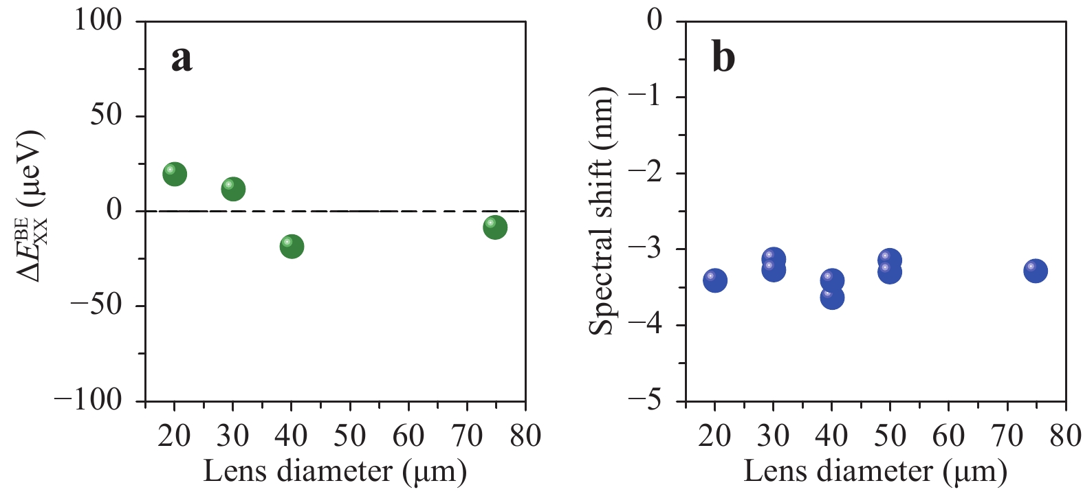
Fig. 6
a Change in the XX binding energy$ \varDelta E $ As already mentioned, the h-SIL leads to an increase in light extraction with a change in the TIR condition. However, the quantitative analysis is not obvious and requires further clarification, as the PL intensity ratio between different energy states of the QD might change after 3D printing of the SIL. This can be observed in Fig. 5 for the exciton (X) and charged exciton (CX) lines. As previously described, h-SILs have a focusing effect on the excitation laser beam. The consequence is a different power density at the QD site. This can affect trapped charges in the QD vicinity, thus modifying the internal quantum efficiency21,48, which leads to a definition of the PL intensity ratio of
$$ \tilde \eta = \frac{{I_{\rm{X}}^{\rm{a}} + \mathop \sum \nolimits_i I_{{\rm{C}}{{\rm{X}}_{\rm{i}}}}^{\rm{a}}}}{{I_{\rm{X}}^{\rm{b}} + \mathop \sum \nolimits_i I_{{\rm{C}}{{\rm{X}}_{\rm{i}}}}^{\rm{b}}}}$$ (6) Here,
$ {I}_{\rm{X}} $ represents the integrated exciton intensity, while$ {I_{{\rm{C}}{{\rm{X}}_{\rm{i}}}}} $ stands for the integrated intensity of the i-th charged state. The superscripts a and b represent intensities after and before SIL fabrication, respectively. Furthermore, the XX and higher transitions, if appearing, are not included in Eq. 6. The enhancement factor stems only from transitions saturating at the same excitation power level, which provides a reliable estimation of the PL intensity ratio$ \tilde {\eta } $ . To exclude errors from the setup alignment for the measurements before and after fabrication, a reference structure was fabricated on the same chip. This reference must not have any surface modification on top of the QD. By applying Eq. 6 on the reference QD in saturation, a correction factor$ \alpha $ was determined to account for small variations in the setup alignment. The use of a reference emitter makes it easy to compare results from different setups, even when using different collection NAs. Therefore, we can correct Eq. 6 to$$ \tilde \eta = \frac{{I_{\rm{X}}^{\rm{a}} + \sum\nolimits_i {I_{{\rm{C}}{{\rm{X}}_{\rm{i}}}}^{\rm{a}}} }}{{I_{\rm{X}}^{\rm{b}} + \sum\nolimits_i {I_{{\rm{C}}{{\rm{X}}_{\rm{i}}}}^{\rm{b}}} }} \cdot \alpha $$ (7) By applying this data analysis to the spectra visible in Fig. 5, it is possible to extract a value for this fabricated h-SIL (diameter 30 µm) of
$ \tilde {\eta }=2.19\pm 0.16 $ . In this case, the correction factor was found to be$ \alpha =0.87 $ . All lenses mentioned in Tab. 1 were investigated in the same manner. The corresponding PL intensity ratios are depicted in Fig. 7 and labelled with the corresponding placement error. An average PL intensity ratio of$ \tilde {\eta }=1.99\pm 0.21 $ was determined.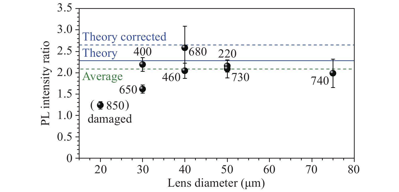
Fig. 7 PL intensity enhancement factor plotted over the SIL diameter.
The numbers next to the data points represent the refraction-corrected displacement values from Tab. 1. The green dashed line marks the average enhancement factor of 2.09. Corresponding theoretical calculations are shown in blue. The solid curve represents the expected PL intensity ratios without considering reflections at the interfaces ($ \tilde {\eta }{{ =2.28}} $ $ {\tilde {\eta }}_{{corr}}{{=}}{2.65} $ Further structural investigations pointed towards the smallest h-SIL being damaged, thus not delivering a perfectly hemispherical shape (see SEM image in Fig. 8a). When excluding the measurement point from the data evaluation in Fig. 7, the average enhancement factor was found to be
$ \tilde {\eta }=2.09\pm 0.23 $ (indicated by the dashed green line). This matches the theoretically calculated value of 2.28 (solid blue line) quite well, assuming perfect transmission at the interfaces. The deviation from the calculated reflection-corrected factor (dashed blue line) can be attributed to uncontrolled diffraction resulting from surface roughness.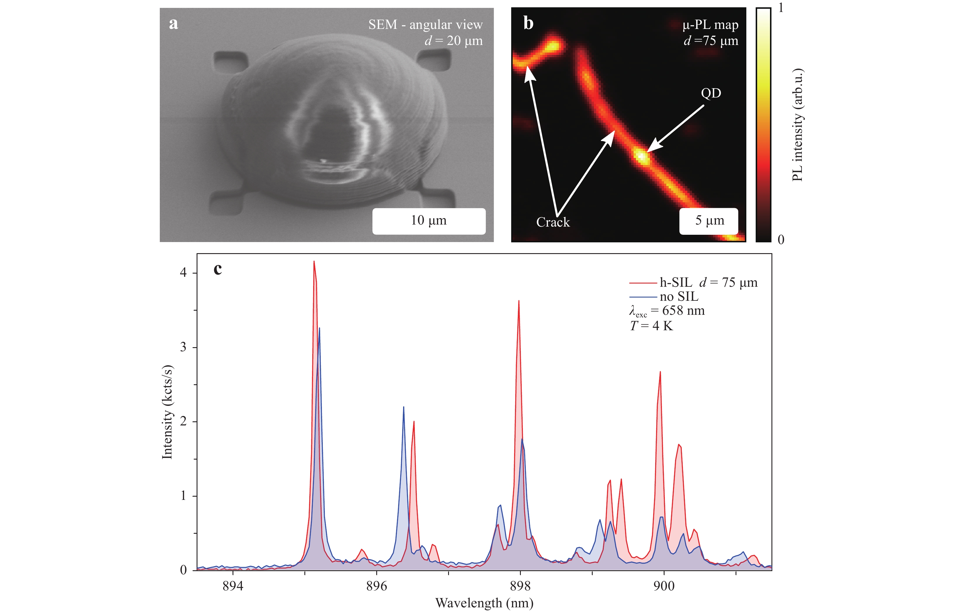
Fig. 8
a SEM image of the excluded broken h-SIL in Fig. 7. Parts of the lens are cracked and peeled off, most likely as a result of the cooling cycle to 4 K. b µ-PL intensity map of QDs underneath a cracked lens. The cracks are visible because of scattering of emitted QD light. Cracks most likely occur at the SIL-GaAs interface because of the lens shrinkage when cooled to cryogenic temperatures. An 865 nm longpass filter was used to suppress the wetting layer signal. c Spectral comparison of a QD underneath a cracked lens with a diameter of 75 µm at 4 K. Spectral shift and PL intensity enhancement are not observable here.These surface variations are on the order of several tens of nanometres and are thus not completely negligible. This can negatively influence lens performance. It is also worth mentioning that the smallest lens was the only small one that was partially damaged. Large lenses exceeding diameters of 75 µm and above are not suitable for low-temperature experiments because they crack during the cooling because of the induced amount of strain at the lens-GaAs-interface. This leads to defects or slight detachment, which results in the SIL not working properly. An example µ-PL scan of a QD underneath a cracked lens can be observed in Fig. 8b. Here, light emitted by QDs is scattered at the cracks, which limits the SIL performance. A further indication for the lens detachment is the absence of the expected spectral blue shift, which is shown in a spectral comparison (Fig. 8c) for the same lens investigated in Fig. 8b.
-
The investigated h-SILs exhibited good intensity enhancement. However, there are geometries that are much more promising. To boost the collection efficiency even further, in the second device generation, the lens geometry was changed to the so-called Weierstrass or hyperspherical geometry. In this case, the lens has the shape of a truncated sphere with a height of
$ R\left(1+1/{n}_{\rm{SIL}}\right) $ ,$ {n}_{\rm{SIL}} $ representing the refractive index of the lens material and$ R $ the radius. A schematic of the Weierstrass geometry used in this work with$ {n}_{\rm{SIL}}=1.51 $ is shown in Fig. 9.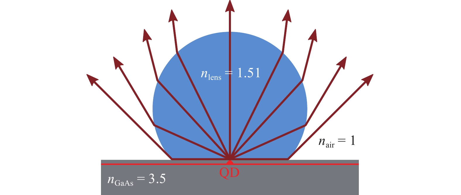
Fig. 9 Schematic of a SIL in the Weierstrass geometry.
All rays leaving the semiconductor are redirected into an output NA, which is only dependent on the refractive index of the lens material.Performing calculations analogously to those previously discussed leads to the collection efficiencies displayed in Fig. 10a. The maximum integration angle for the Weierstrass SIL (W-SIL)18 can be expressed as
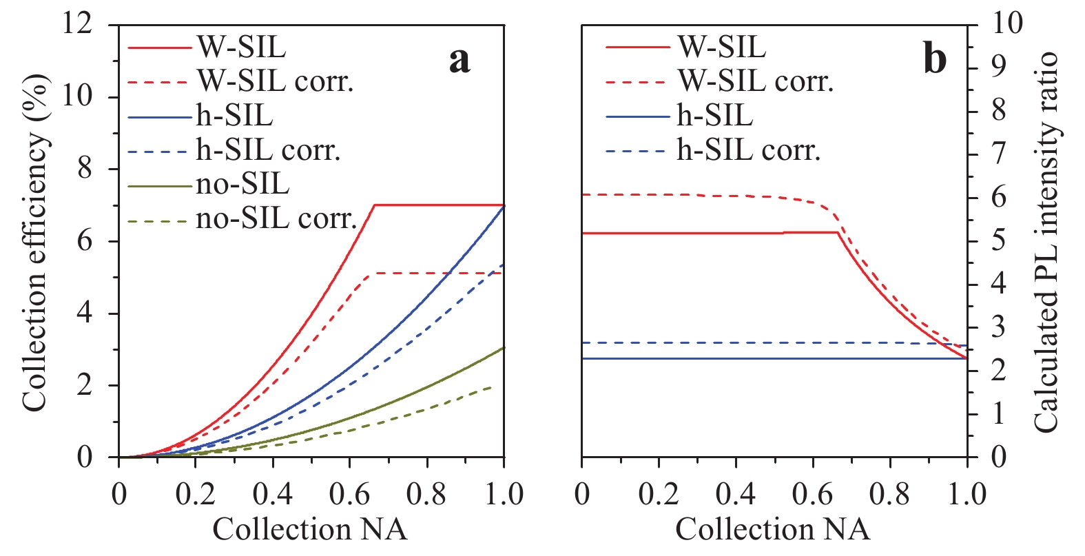
Fig. 10
a Calculated collection efficiencies for planar extraction and extraction from a W-SIL or an h-SIL placed centred above the emitter as a function of the detector collection NA. b Calculated PL intensity ratios for a W-SIL and an h-SIL geometry versus the detector collection NA. The curves are obtained by division of the respective collection efficiency with the W-SIL by the planar one in a. Solid curves represent ideal values, while dashed curves correct for one reflection at the present interfaces (labelled as “corr.”). Here, refractive indices of$ {n}_{\rm{GaAs}}=3.5 $ $ {n}_{\rm{SIL}}=1.51 $ $ {n}_{\rm{air}}=1.0 $ $$ \theta _{{\rm{max}}}^{{\rm{W - SIL}}} = {\rm{arcsin}}\left( {\frac{{n_{{\rm{SIL}}}^2}}{{{n_{{\rm{GaAs}}}}}} \cdot NA} \right) $$ (8) The curves of the W-SILs can be interpreted such that all the light that exits the semiconductor and enters the lens is folded into a certain output NA, which is only dependent on the refractive index of the Weierstrass lens. For a refractive index of
$ {n}_{\rm{SIL}}=1.51 $ , this critical NA value is 0.66. This is verified by taking a closer look at the non-reflection-corrected curves in Fig. 10. Here, both solid curves of h- and W-SIL intersect at$ {\rm{NA}}=1.0 $ , yielding the same overall collection efficiency. The refraction-corrected curve ends up at a slightly lower value than that for the h-SIL, which is expected. For an h-SIL, all angles of incidence at the lens-to-air interface are in good approximation zero, which leads to the highest possible transmission. As Fig. 9 illustrates, this is not the case for the W-SIL, where strong refraction leads to significant Fresnel losses.This indicates the expected PL intensity enhancement values of
$ {\tilde \eta _{{\rm{ideal}}}} = 5.20$ and$ {\tilde \eta _{{\rm{corr}}}} = 6.02 $ for detector collection NAs between 0 and 0.66, as shown in Fig. 10b. For higher NAs, the PL intensity ratio$ \tilde {\eta } $ converges towards the ratio for h-SILs, as expected. According to the spectral comparison shown in Fig. 11, a clear enhancement of all emission lines is observable, as well as the typical expected blue shift of approximately 3 nm. In this case, characterisation before and after SIL placement was carried out in a standard free-space µ-PL setup with a detection collection NA of 0.45 under continuous-wave (CW) excitation with a laser using an emission wavelength of 632 nm. Performing the data analysis on the X and CX emission lines, as in Section 3.1, resulted in a measured PL intensity ratio of$ \tilde {\eta }=3.85\pm 0.45 $ . This value deviates significantly from the theoretically expected enhancement factor of approximately 6 for a detection collection NA of 0.45. However, this behaviour can be explained by looking at the investigated W-SIL shape and surface structure in Fig. 12.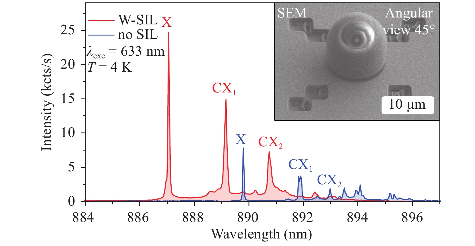
Fig. 11 µ-PL spectra of the same QD underneath a Weierstrass lens with a diameter of 10 µm and without a lens.
Emission characteristics were identified prior to the intensity enhancement evaluation via power-dependent measurements. The inset depicts a SEM angular view picture (45° tilt) of the printed W-SIL.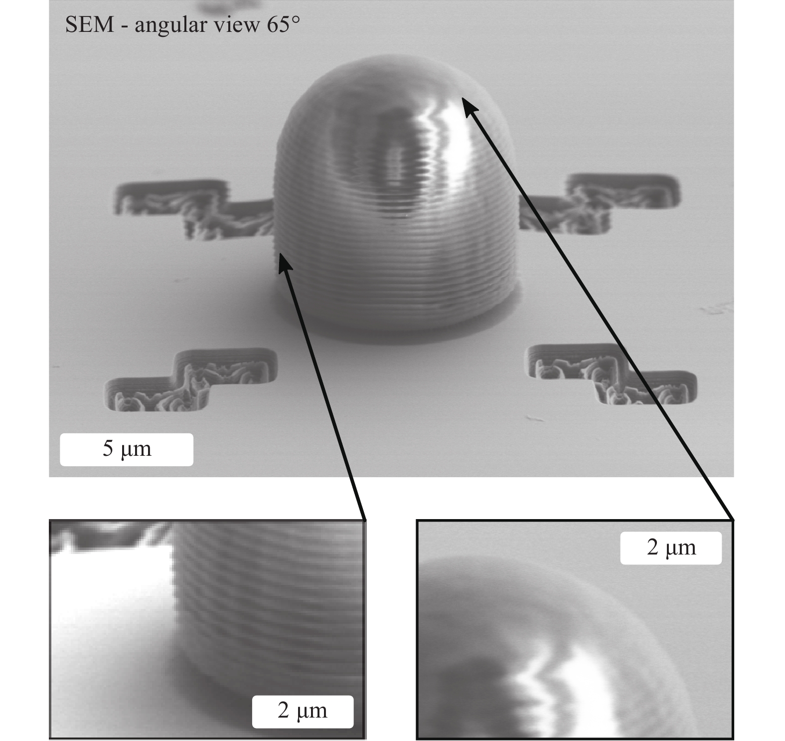
Fig. 12 SEM angular view picture (65° tilt) of the same W-SIL depicted in the inset of Fig. 11.
Severe surface roughening is observable at steeper surfaces (lower left image), while curved surfaces show less roughness (lower right image). Additionally, the lower shape deviates from the nominal Weierstrass geometry.When investigating the lens shape via scanning electron microscopy (SEM) in angular view (65° tilted), it can be seen that the shape does not perfectly correspond to the Weierstrass geometry. Indeed, the lower part differs considerably from the ideal shape, which causes losses because refractions do not fold the light into small NAs. In addition, severe surface roughening is also visible in the lower left image in Fig. 12, which is on the order of several tens of nanometres, up to 100 nm. This causes uncontrolled diffraction, which also limits the lens performance and explains the deviation from the theoretically expected value of approximately 6. However, the apex of the lens seems to be quite smooth (lower right SEM image in Fig. 12). Assuming the same placement accuracy as for the h-SILs, this may also be one of the limiting factors, as the Weierstrass geometry is considered to be much more sensitive to the emitter position. Another W-SIL with the same shape as demonstrated in Fig. 12 was investigated and showed a PL intensity enhancement of only
$ 2.51\pm 0.10 $ , which is assumed to occur as a result of an even larger lens displacement. -
The W-SIL results showed that much higher values of collection efficiencies can be achieved with more complex lens geometries than an h-SIL and that care must be taken to avoid roughness or deviation from the optimal design. For this reason, we developed an advanced SIL design, referred to as TIR-SIL. This geometry makes use of the total internal reflection condition at the SIL-to-air interface. A cross-sectional illustration that takes ray tracing calculations (with the commercially available software OpticStudio) into account is shown in Fig. 13.
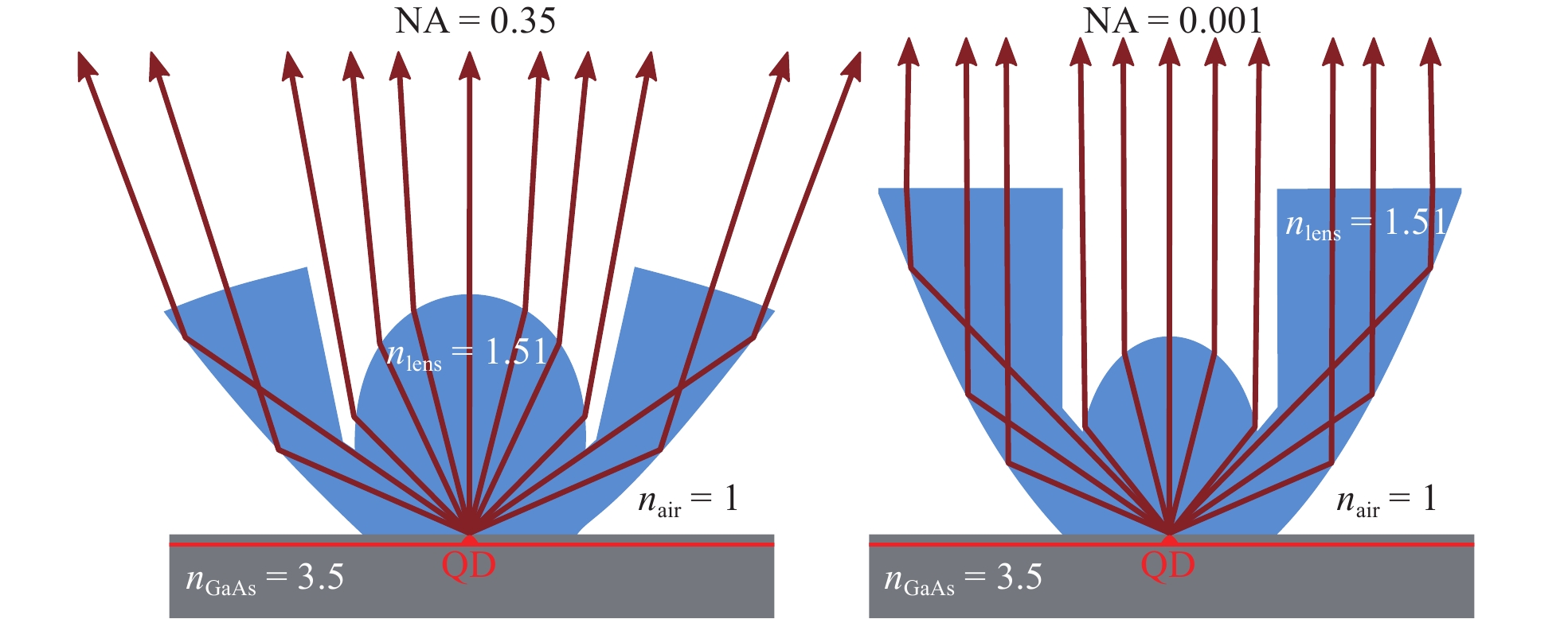
Fig. 13 Cross-sectional sketch of the working principle of a TIR-SIL, which folds all the light leaving the semiconductor into a predefined NA.
Reflections and refractions were calculated for this illustration with the commercially available ray tracing software OpticStudio. (left) TIR-SIL designed for NA = 0.35. (right) TIR-SIL designed for NA = 0.001.The TIR-SIL is composed of an inner aspheric lens and an outer parabolic reflector structure. The reflector makes use of the TIR condition at the lens-to-air interface, as can be seen in Fig. 13. By engineering both components, all the light can be folded into arbitrary output NAs. Because TIR is quite sensitive to the angle of incident light, a small lateral emitter misplacement is expected to affect the extraction more negatively compared with the h-SIL and W-SIL geometries. Thus, losses are induced in the form of light being refracted, instead of fully reflected. Choosing this TIR-SIL geometry can be interpreted in such a way that the kink in the efficiency curve of the W-SIL is shifted in the horizontal direction towards smaller NAs, depending on the lens design. This is illustrated (not calculated) in Fig. 14 for a designed NA of 0.35. The green sections of the curves can be calculated from the lens design. The grey sections are justified based on the similarity of the inner Weierstrass-like lens shape.
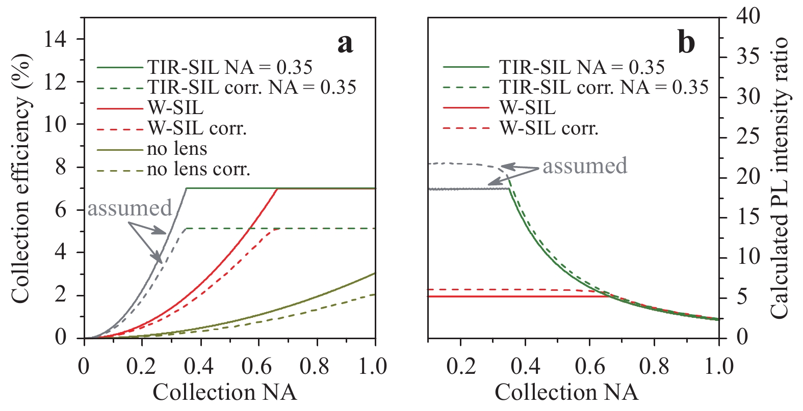
Fig. 14
a Collection efficiencies for planar samples, W-SILs, and TIR-SILs (output NA of 0.35) versus the detector collection NA. b PL intensity ratios for W-SILs and TIR-SILs (output NA of 0.35) versus the detector collection NA. The curves are obtained by division of the respective collection efficiency with the TIR-SIL by the planar one in a. Solid curves represent ideal values, while dashed curves correct for one reflection at the present interfaces (labelled as “corr.”). The assumed continuation of the curves for the TIR-SIL geometry for NAs lower than 0.35 is based on the similarity of the inner Weierstrass-like lens shape and plotted in grey.In this work, two TIR-SIL geometries with different output NA designs were fabricated. Both are illustrated in Fig. 13:
$ {\rm{NA}}=0.35 $ (left) and$ {\rm{NA}}=0.001 $ (right). Investigation of the TIR-SIL (see Fig. 15) with an NA of 0.35 resulted in a blue shift of 2.82 nm (4.4 meV). This lies within the typical range for QDs underneath 3D printed objects with contact surfaces in this size range. With the same data evaluation as before, a PL intensity enhancement of$ \tilde {\eta }=5.61\pm 0.14 $ (collection objective$ {\rm{NA}}=0.45 $ ) was determined. Theoretical values of$ {\tilde \eta _{{\rm{ideal}}}} = 11.30$ and$ {\tilde \eta _{{\rm{corr}}}} = 11.96 $ for a detector collection NA of 0.45 were extracted from the curves in Fig. 14.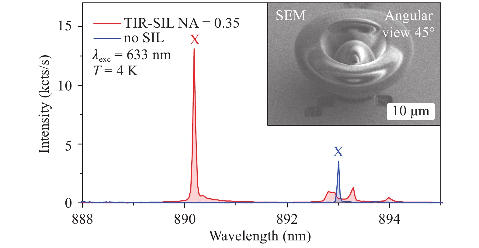
Fig. 15 µ-PL spectra of the same QD underneath a TIR-SIL designed for an NA of 0.35 with a bottom diameter of 10 µm and without a lens.
A blue shift of the main emission line of 2.82 nm is observable, while the intensity is enhanced by a factor of$ \tilde {\eta }{ =}{ {5.61\pm 0.14}} $ The rather large deviation of the measured value from the theoretically expected one can be explained by the surface roughness of the printed material (see Fig. 12), probably as a result of the non-ideal placement of the lens. In addition, the same QD below the lens was used to perform an autocorrelation measurement under pulsed excitation at 650 nm on the brightest line in saturation. This resulted in the histogram displayed in Fig. 16. A binning of 7 ns gives a
$ {g}^{\left(2\right)}\left(0\right) $ -value of$ 0.19\pm 0.01 $ , which is a clear indicator of single-photon emission. Although the QD experiences massive strain during cooling down after 3D printing, the single-photon character of the emission is maintained.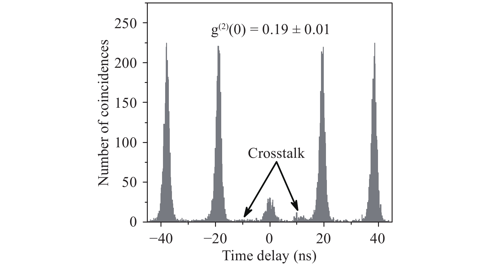
Fig. 16 Autocorrelation measurement of the main emission line of Fig. 15 under pulsed excitation at 650 nm.
For the$ {\rm g}^{\left(2\right)}\left(0\right) $ $ {\rm g}^{\left(2\right)}\left(0\right)=0.19\pm 0.01 $ To acquire further statistics for the TIR-SILs, several SILs folding the light into an NA of 0.001 for quasi-collimated output were 3D printed while being aligned on the pre-selected QD positions. Fig. 17 displays two spectra from the same QD, before and after 3D printing. Again, a blue shift of 3.43 nm (5.42 meV), which is comparable with previously achieved results, can be observed. A PL intensity ratio of
$ 8.33\pm 0.39 $ was found for this lens. The inset shows an angular SEM image (45° tilt) of the lens design. It is aligned here on etched markers, even though the spectrum belongs to a QD marked with metal markers. By deposition of metal markers, distortion of the alignment laser beam at the marker edges can be avoided. Therefore, an improvement in the alignment accuracy of the 3D direct laser writing machine is expected. Five TIR-SILs were fabricated in total, only one of them with etched markers. Analysis of this lens also resulted in the lowest enhancement factor (see Fig. 18) because it is more difficult to align the laser of the 3D printing machine on these markers. For the other four lenses, Cr/Au markers were deposited. A maximum PL intensity ratio of$ 9.72\pm 0.82 $ was observed here, underlining the use of metal markers and the sensitivity of the enhancement factor with respect to the accuracy of the lateral lens placement. On average, a PL intensity enhancement ratio for this lens geometry of$ \tilde {\eta }=7.24\pm 0.49 $ was determined, which is marked by the black dashed line in Fig. 18. The calculated enhancement factors are illustrated in blue.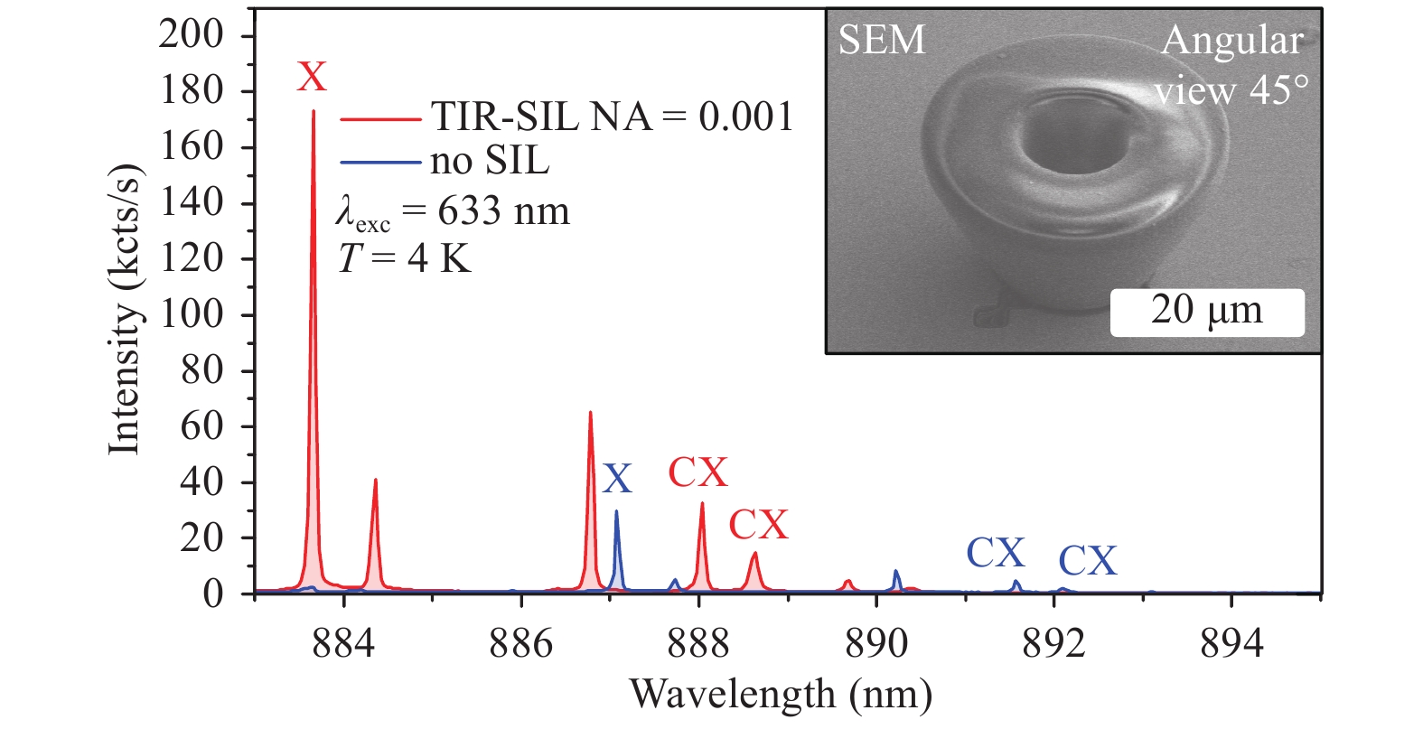
Fig. 17 µ-PL spectra of the same QD underneath a TIR-SIL designed for a NA of 0.001 with a bottom diameter of 10 µm and without a SIL.
Emission characteristics were identified prior to the intensity enhancement evaluation via power-dependent measurements. The inset shows an SEM angular view image (45° tilt) of the printed TIR-SIL designed for folding all the light leaving the GaAs into an NA of 0.001.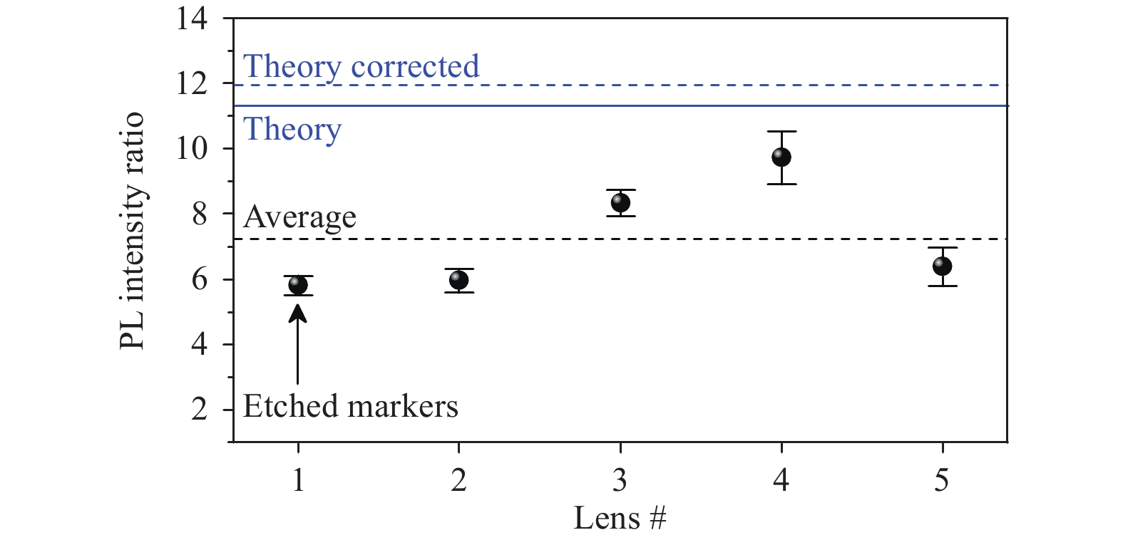
Fig. 18 PL intensity ratios for a total of 5 printed TIR-SILs, which fold all light into an NA of 0.001.
Lenses yield an enhancement of between approximately 6 and 10. The lateral position of the first lens was determined using etched markers, while all other lenses were positioned using metallic markers.Tab. 2 gives a final overview of the theoretically expected and averaged measured PL enhancement factors for each fabricated lens geometry. For future applications, the TIR-SIL designed for an output NA of 0.001 offers the most promising results, especially when the 3D printing machine is aligned using metal markers.
Lens type Theoretical PL enhancement Measured PL enhancement h-SIL 2.65 2.09 ± 0.23 W-SIL 6.02 3.18 ± 0.28 TIR 0.35 NA 11.96 5.61 ± 0.14 TIR 0.001 NA 11.96 7.24 ± 0.49 Table 2. Overview of theoretically expected and average measured PL enhancement factors for each fabricated lens type.
To compare our TIR geometry (
$ {\rm{NA}}=0.001 $ ) with the aspheric geometry introduced in22, we also estimated the collection enhancement for a collection objective NA of 0.1. With our geometry, a value of approximately 66 can be obtained, which is similar to the reported factor of approximately 100. Bogucki et al. obtained a maximum collection efficiency of 6.1% for a collection NA of 1, which is comparable with the values reported in this work (compare Fig. 10 and Fig. 14). However, the TIR geometry allows for the collection of that amount of the extracted light for arbitrary small NAs and provides the possibility of shaping the emitted light cone to match the in-coupling lens, 3D printed on a fibre tip, which will be the subject of the next section. -
After evaluating the different micro-lens designs, we now focus on the fabrication of a single-mode fibre-coupled standalone single-photon device based on 3D direct laser writing. For this purpose, we developed a design for a 3D printed fibre chuck. The working principle is illustrated in Fig. 19. Fig. 19a illustrates the chuck and fibre before mating. The mating is performed with a manual XYZ flexure stage under a microscope. The guideway is highlighted by the dashed lines in Fig. 19a. The narrower diameter at the lower level ensures a fixed vertical alignment, while the higher-level tube serves as a restriction in the lateral degree of freedom. After the lateral alignment, the fibre is inserted into the chuck, which can be seen in the intermediate microscope picture in Fig. 19b. Once the fibre cannot be moved any further (Fig. 19c), the mating is complete and epoxy glue is applied to fix the fibre to the 3D printed structure.
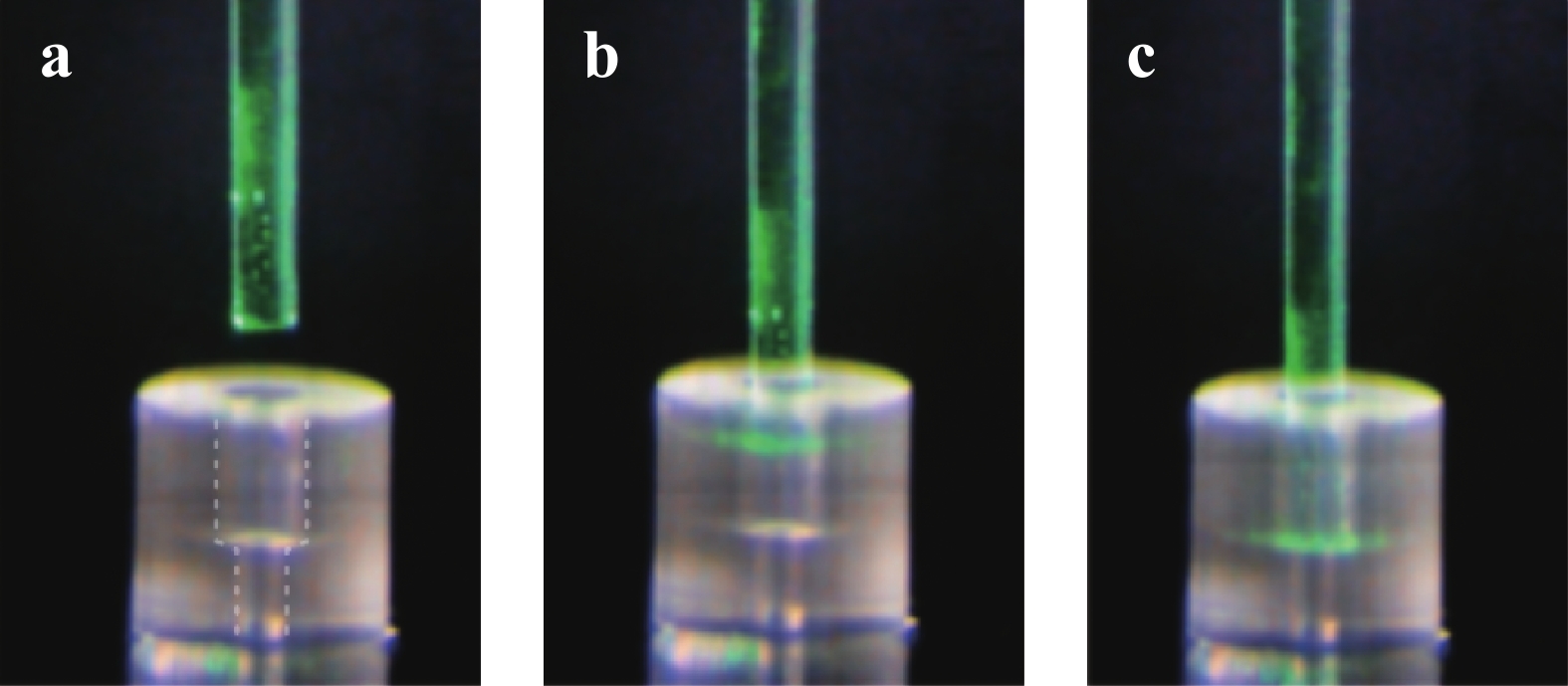
Fig. 19 Different stages of the fibre mating process recorded as a sequence of microscope pictures.
a The fibre is aligned on the opening hole of an exemplary chuck. b Intermediate snapshot of the mating procedure while the fibre is moved towards the stopping level. c Completed fibre mating. The fibre is stopped via the step indicated in a. by the dashed white lines and is ready for being fixed with epoxy glue.The entire structure is built on the precise knowledge of the location of a QD, provided by the deposition of metal markers, and the 3D direct laser writing of a TIR-SIL. To properly align the large chuck to the lens position, the step in which the TIR-SIL is printed has to be slightly adapted. The lateral lens dimensions are so large that the metal markers are no longer visible after 3D printing. Therefore, the fabrication of the lens is supplemented by simultaneous 3D printing of another set of large standard markers at a distance of a few micrometres. An example microscope image of a TIR-SIL with the 3D printed markers is shown in Fig. 20. The chuck printing step is then aligned to the 3D printed markers, and a conical in-coupling lens is additionally printed on the fibre tip, as sketched in Fig. 21a. This lens is designed for refracting the incident QD emission into the acceptance NA of the single-mode fibre (SM-780HP, NA = 0.14). Here, the sketched TIR-SIL
$ ({\rm{NA}}=0.001) $ is aligned on the QD position. In the second step, a large fibre chuck is printed to be aligned on the position of the printed lens. Its design is composed of a larger lower stage to ensure good contact with the sample surface. The chuck becomes thinner above a height of 100 µm. Pipes are included in the design to enable the He exchange gas used inside the bath cryostat to enter the chuck and fill the space between the TIR-SIL and modified fibre tip. A stopping level was introduced to precisely control the distance between the 3D printed lens and modified fibre tip. The upper section is designed to match the diameter of the fibre to control the lateral alignment. When the alignment is finished, the fibre and chuck are fixed using epoxy glue, as shown in Fig. 21b. In this experiment, the epoxy glue unfortunately also covered the gas exchange channels (Fig. 21). They were implemented with the idea of avoiding humidity and air freezing inside the device during the cooling cycle. Air inside the chuck is supposed to be evacuated when the sample is placed into a cryostat. Because this was not possible in this experimental round, the device performance was limited. For the sample characterisation, the fibre-coupled QD single-photon source was mounted in the deterministic lithography setup, as shown in Fig. 22.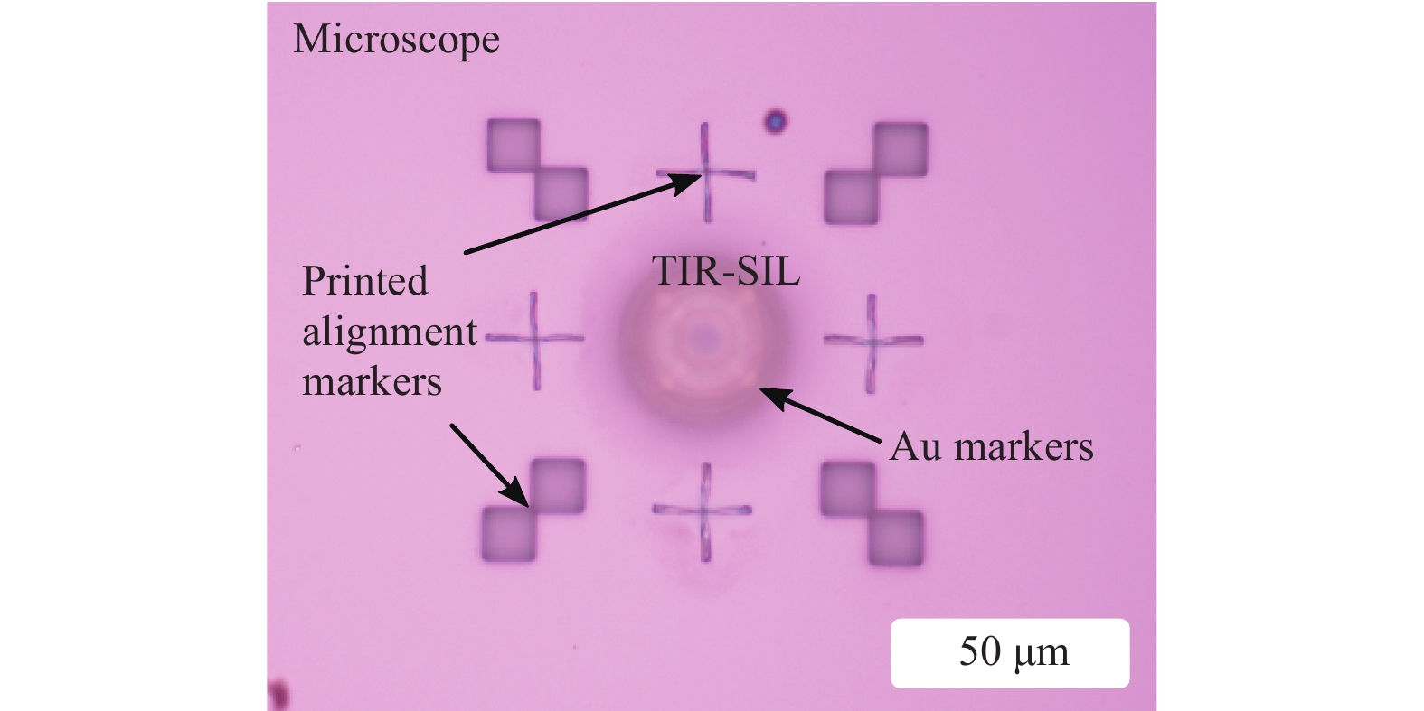
Fig. 20 Microscope image of a TIR-SIL designed for an NA of 0.001.
Alignment markers were printed in the same process step with the scope of later alignment for the fibre chuck printing. Deposited Au markers are still partly visible underneath the TIR-SIL.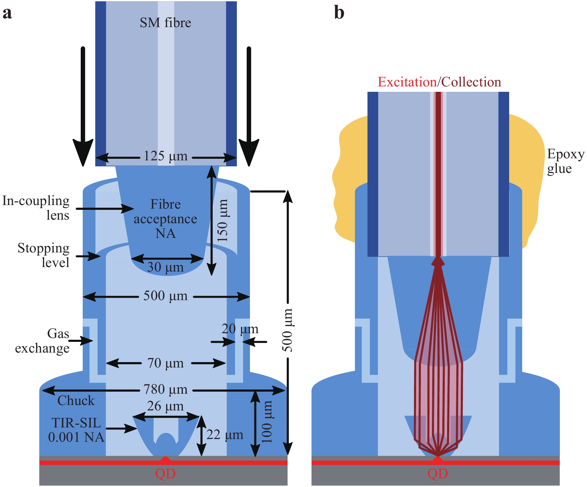
Fig. 21 Schematic of the final fibre chuck design.
a A TIR-SIL with an NA of 0.001 is printed, deterministically aligned on the QD position. After the characterisation of the printed lens, the big tube-like chuck is fabricated, being aligned on this lens. On the fibre tip, another lens is printed for coupling the modified emission into the fibre core. The modified fibre is then inserted into the chuck. Typical dimensions of the 3D printed parts are respectively labelled. b Epoxy is used to fix the fibre position. Excitation and collection of the QD are carried out via the same fibre, here illustrated as light red (excitation) and dark red (collection).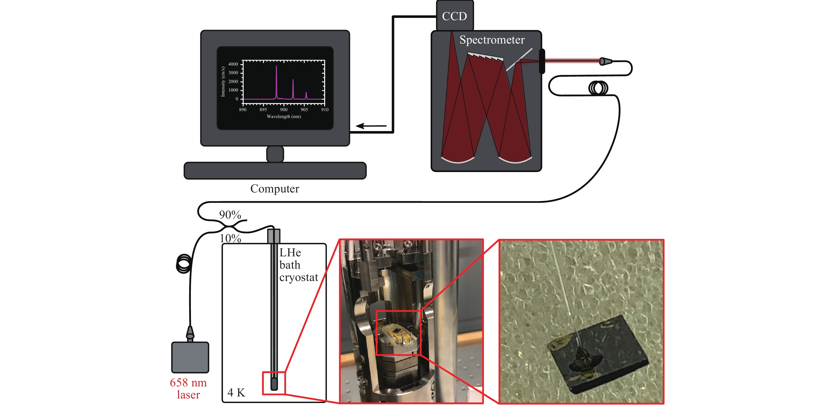
Fig. 22 Setup configuration for characterisation of the standalone fibre-coupled device.
Excitation takes place via a fibre-coupled laser diode at 658 nm sent through a 90:10 beam splitter and a fibre throughport connected to the sample. Light emitted by the QD is guided via the 90% channel to the spectrometer and recorded via a CCD on the computer.The red box indicates the mounted sample in more detail. On the bottom right, the standalone device is displayed completely covered in epoxy, which provides robustness in terms of mechanical stability when mounted. It is then glued to the sample holder and placed inside the setup as in the mid-bottom inset in Fig. 22. The fibre throughport installed at the top of the setup ensures the fibre connection from the red excitation laser to the sample and back to the spectrometer via a 90:10 beam splitter. All fibres are connected in such a way that only 10% of the QD emission is lost at the beam splitter. After cooling down to 4 K, the QD is excited through the fibres with a laser module emitting at 658 nm, and the emission is guided back to the spectrometer. Because of its high brightness and clean spectrum, the QD investigated in Fig. 17 was chosen as the ideal candidate for the fibre mating experiment. The investigation resulted in the spectra shown in Fig. 23a and b. It is directly visible from the left spectrum that, because of the large 3D printed chuck, even more strain is induced as a result of contraction of the lens material at low temperatures.
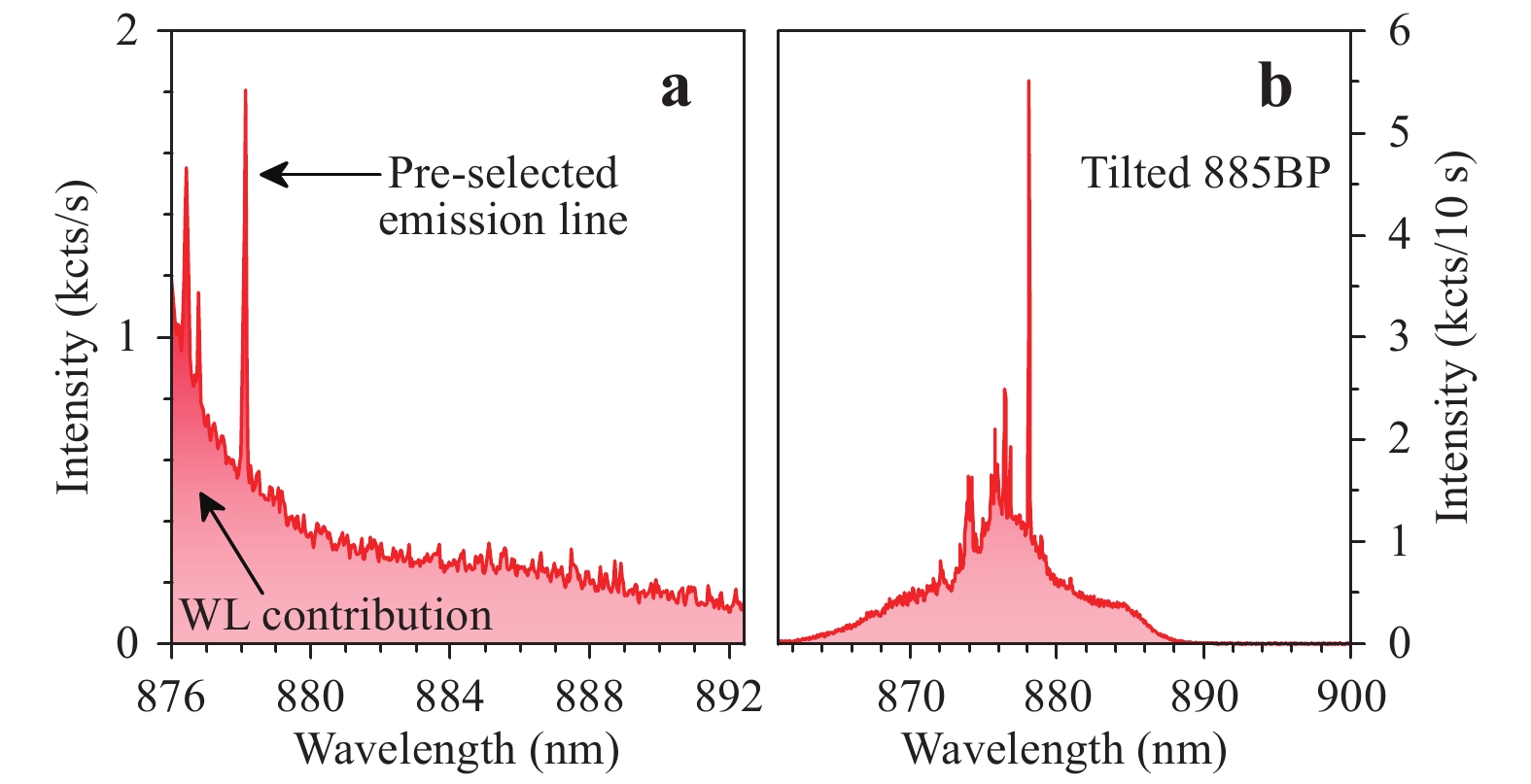
Fig. 23
a Unfiltered PL signal of the standalone QD device. b Spectrum filtered with a band-pass filter that is designed for 885 nm ± 12.5 nm. Tilting the filter shifts the wavelength window down to lower wavelengths. The large printed chuck induces additional strain on the QD, causing a further blue shift of the emission to the edge of the wetting layer. Both spectra were acquired in saturation. The QD with the spectrum in Fig. 17 was used for fibre mating. -
The brightest emission line in Fig. 23a is located at 878.12 nm. Unfortunately, the spectrum could not be directly reproduced because the strain was so large that the QD emission shifted to the tails of the wetting layer. The further blue shift could only be roughly estimated (5.55 nm, which equals 8.9 meV) by investigating the brightest observable emission line. It can be concluded that the lens and the chuck induce a blue shift of approximately 9 nm on pre-selected QDs in this emission wavelength range (energy of approximately 13 meV). Similar to previous estimations of the present stress on the QD, a strain of approximately 468 MPa can be derived46,47. For further experiments and applications, this shift has to be considered in the QD pre-selection step by selecting QDs with emission wavelengths far away from that of the wetting layer. To partially suppress the wetting layer contribution when acquiring a spectrum where the emission line is spectrally in the centre of the investigation, a band-pass filter (885BP) was placed inside the detection path in front of the spectrometer entrance. By tilting this filter, the transmission window could be shifted toward shorter wavelengths. This suppresses the large contribution on the lower wavelength side from the wetting layer and results in the spectrum visible in Fig. 23b (integration time: 10 s).
Comparing the integrated intensity of the coupled QD light from Fig. 23a with the integrated intensity before the chuck fabrication (Fig. 17) resulted in a total coupling efficiency of approximately 1.05 ± 0.18%. One factor that might inhibit the in-coupling efficiency is a non-perfect alignment between the fibre lens and TIR-SIL, possibly induced by the cooling process. Because of the circular symmetric chuck design, the effect of material contraction when cooling is not expected to induce displacement of the components in the lateral direction. Nevertheless, a change in vertical spacing seems likely. Additionally, the material contraction of the optical elements, as well as the thermo-optical effect, have to be taken into account, as they influence the focal length of the fibre lens. In addition to these issues, the surface roughness of the lenses or the displacement of the in-coupling lens with respect to the single-mode fibre core might contribute to the losses. To gain a better understanding of the limiting factors, we validated the in-coupling efficiency achievable with the current lens design using another QD sample without a chuck and performing an in-situ alignment of the fibre and TIR-SIL. As illustrated in Fig. 24a, the QD sample can be moved in relation to the fibre in a high-stability bath cryostat while monitoring the in-coupling signal. In this way, we eliminate the displacement between the fibre and TIR-SIL by aligning to the maximum signal. Fig. 24b compares the QD spectra without any lens to the fibre-coupled signal obtained by this method. Performing the same analysis that was used previously for the evaluation of the h-SILS, we found an in-coupling efficiency of 26 ± 5%, corresponding to an increase by a factor of greater than 20 compared with our first result. From this, we conclude that precise positioning of the fibre via the 3D printed chuck is crucial for the performance of our system. A fully integrated device using a glued fibre chuck yielding the same efficiency (corresponding to a maximum single-photon rate of 1.5 Mcounts / s) was realised recently in41. In the same work, successful Hanbury-Brown and Twiss measurements were performed, which resulted in a
$ {g}^{\left(2\right)}\left(0\right) $ -value of 0.13 ± 0.0541, confirming the single-photon nature of the fibre-coupled emission. In the future, in-coupling efficiencies might be improved further by addressing the issues mentioned above, such as the influence of the thermo-optical effect, or the positioning of the lens on the fibre.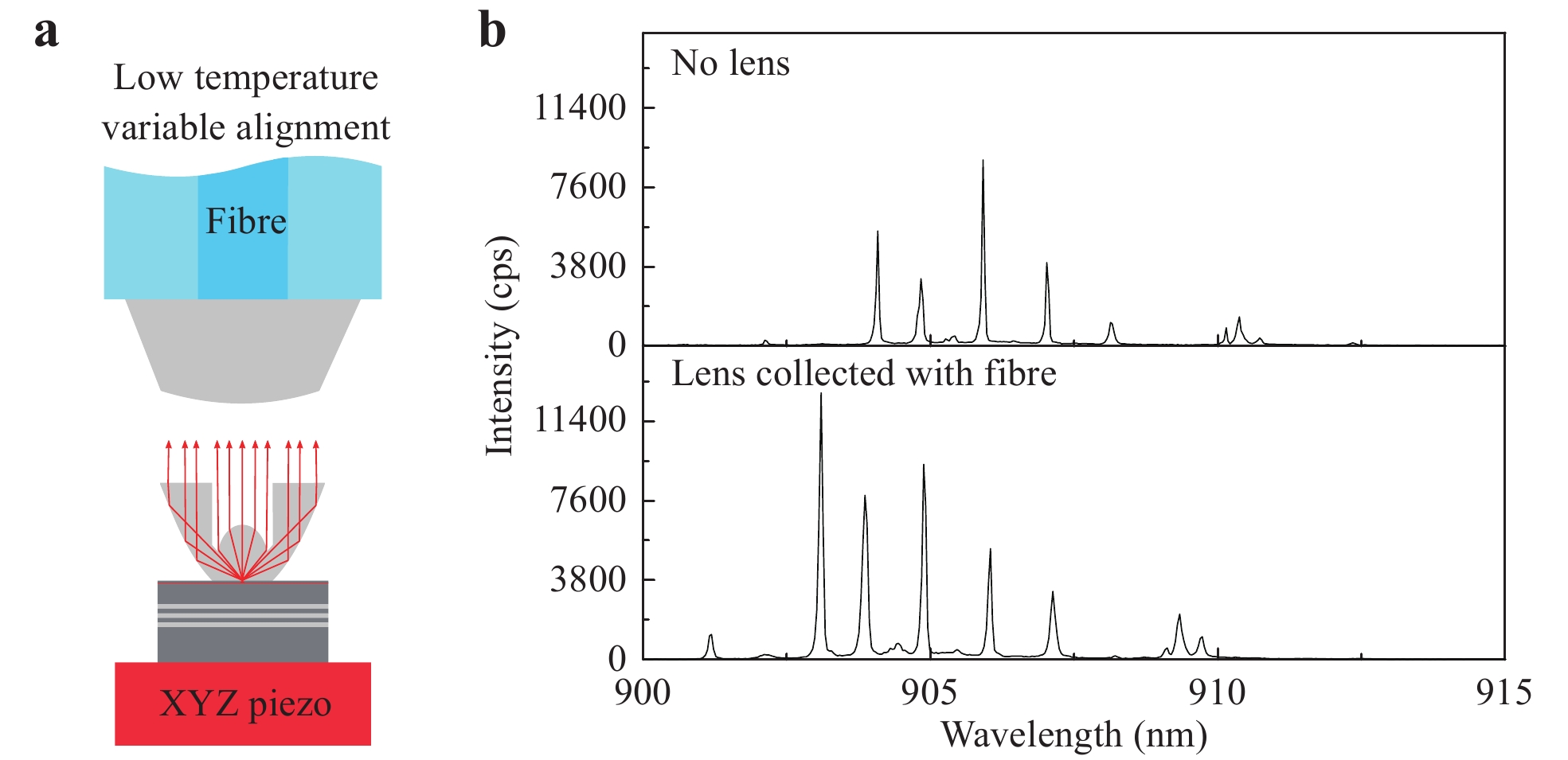
Fig. 24
a Schematic illustration of the measurement principle used to validate the in-coupling efficiency. The sample is mounted onto a high-precision XYZ piezo stage and can thus be moved in all three dimensions in relation to the fibre. b Spectrum of utilised QD before lens printing (top) and maximum fibre-coupled signal (bottom). Spectra are saturated upon above band gap pumping ($ \approx $ -
In conclusion, we successfully developed a reproducible method to enhance the collection efficiency in single QD spectroscopy using a combination of deterministic, optical low-temperature lithography with femtosecond 3D direct laser writing. Here, the 3D printing machine was either aligned on etched markers or deposited metal markers, which proved themselves to be the better choice in terms of the alignment procedure. Different lens shapes were investigated experimentally and compared with calculations. For all lens geometries, an increase in the collection efficiency was confirmed. The simplest geometry, namely h-SIL, resulted in an intensity enhancement of approximately 2.1, which is in good agreement with the performed calculations. Furthermore, the h-SILs seem to be relatively tolerant to displacement errors with respect to the QD position. Despite this, a spectral blue shift resulting from the contraction of the lens material and thus inducing strain on the QD when cooled down to 4 K has to be considered if a specific target emission wavelength is desired. Moreover, the lenses result in a better focusing of the pump laser, which affects the pumping condition, eventually modifying the ratio between different emission lines of the same QD. In addition, an increased signal-to-noise ratio was observed, increasing the localisation accuracy of a QD from 2 nm to less than 1 nm. A further increase in collection efficiency is promised by the Weierstrass geometry, which possesses a hyperhemispherical shape. It offers a more significant modification of the emission, redirecting all the light leaving the semiconductor into a detector collection NA of approximately 0.66. Enhancement factors of up to approximately 3.9 were observable in combination with a typical spectral blue shift. The deviation from the predicted enhancement value can be attributed to a non-ideal alignment of the 3D printer on the etched markers and to a non-perfect lens shape and lens surface roughness, which cause uncontrolled diffraction at the lens-to-air interface. Further improvement was achieved by the development of the TIR-SIL geometry, which consists of a centred aspheric lens and a radial symmetric reflector structure, making use of the TIR condition. This approach has proven to fold the light in even smaller and customisable NAs than achievable for the Weierstrass geometry. Theoretical estimates of the enhancement factor are also greater than the achieved experimental value. Because this lens type relies on the TIR condition, its placement accuracy becomes even more critical than before. Therefore, only one measured value was close to the expected theory. In general, the TIR-SIL reliably provides a PL intensity ratio between 6 and 10, also in combination with an overall spectral blue shift of approximately 5 meV. To summarise, a reliable process was developed to efficiently enhance the collected QD light by a factor of up to 10. Using the TIR-SIL and folding all the light into an NA of 0.001, the idea of a fibre-coupled standalone quantum dot device was partially realised. Because of the large contact area of the fibre chuck and the sample, additional strain was induced, leading to an additional blue shift in the overall emission. Consequently, the spectrum of the one and only device overlapped with the wetting layer. By selecting QDs with a far higher wavelength, this issue can be avoided. The validation of the approach for fibre in-coupling, that is, the use of a QD provided with a TIR-SIL and a fibre with an additional focusing lens, was performed, employing a setup capable of precisely aligning the fibre with respect to the emitter. A value of up to 26% was shown, opening the route to a stable stand-alone, fibre-coupled device41.
In the future, we are going to optimise coupling and add anti-reflection coatings, trying to push the coupling efficiency to the theoretical limit. Furthermore, our technology can be combined with a QD single-photon source based on circular Bragg gratings49,50, NV centres, defects, and other quantum emitters. In addition, a highly efficient combination with single quantum detectors should be feasible.
-
Both samples used in this work are schematically illustrated in Fig. 25 and were grown via metalorganic vapour-phase epitaxy (MOVPE) using the standard Stranski-Krastanov growth mode. The overall structures are similar, in that both are based on the growth of a bottom AlAs/GaAs distributed Bragg reflector (DBR) structure below the InAs QD layer to enhance the emission brightness before the 3D printing of SILs. For details on the sample growth, we refer to Refs. 21,51. Because we concentrate on the PL intensity enhancement and not on directly measuring the collection efficiency or brightness, the number of DBR pairs is actually not decisive. First, the sample was spin-coated with photoresist. It was then mounted with Fixogum, a silicon-based glue, onto a sample holder and placed onto a piezo stack underneath a specially designed low-temperature microscope objective with a numerical aperture of NA = 0.8. The sample was then cooled down to 4 K in a liquid helium bath cryostat, and a low-temperature lithography step was performed. During this step, markers with the shape illustrated in Fig. 26a were defined in the photoresist using an in-situ low-temperature lithography setup as developed and used in Refs. 21,29. After development (see microscope image in Fig. 26b), the markers were transferred onto the sample surface. This was accomplished by inductively coupled plasma reactive ion etching (ICP-RIE) (SEM image in Fig. 26c) or by the deposition of metal via electron-beam evaporation (SEM image in Fig. 26d).
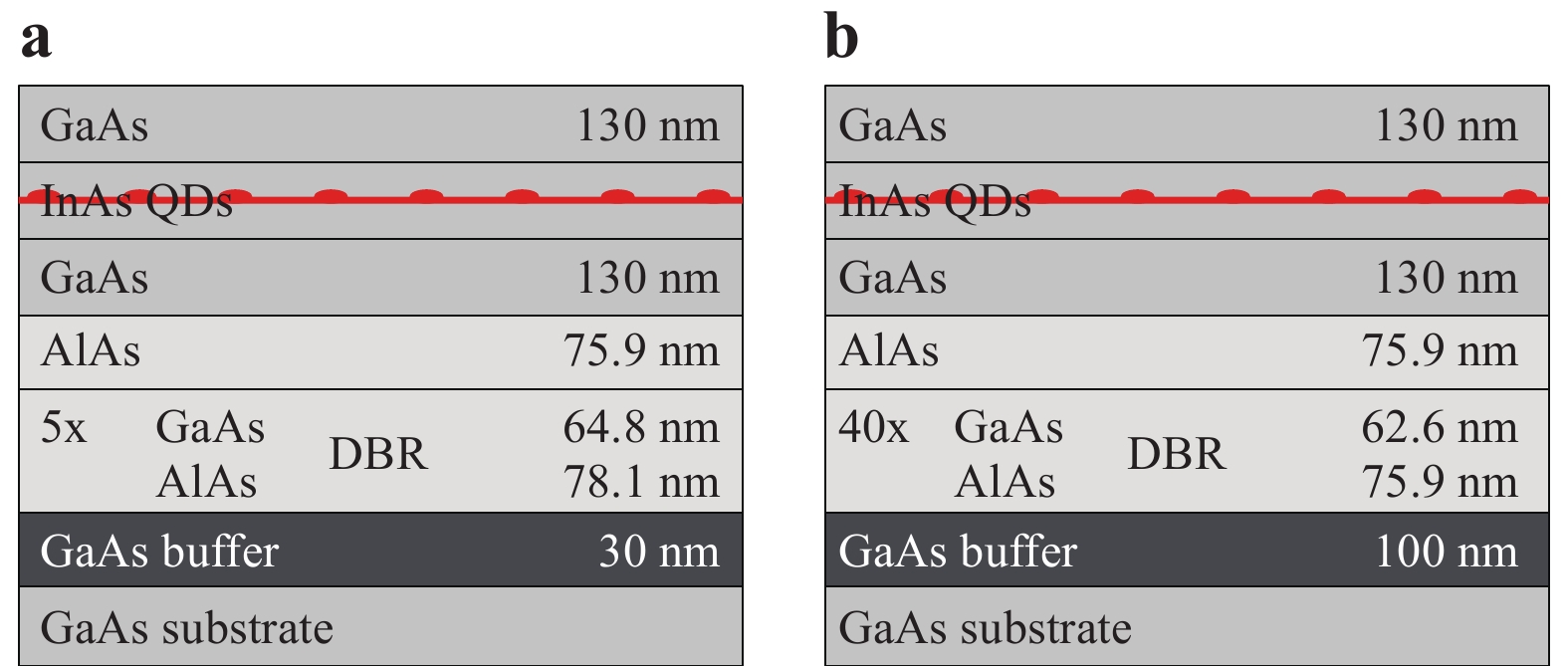
Fig. 25 Schematic of the used sample structures.
For both samples, a bottom DBR was grown to enhance the intrinsic QD brightness. a Used sample structure for the measurements in section 3.1 and 3.2. b Used sample structure for measurements in section 3.3.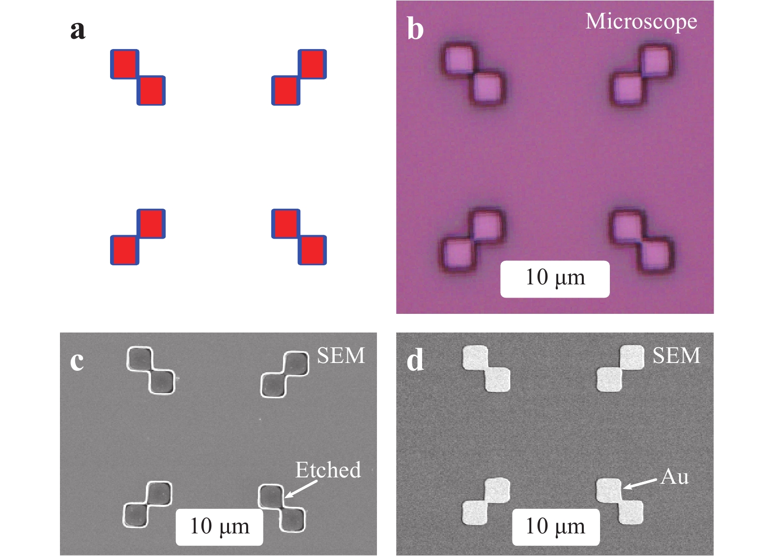
Fig. 26
a Illustration of the marker geometry. b Microscope picture of developed markers after positive lithography process. c SEM picture of markers transferred into the substrate with ICP-RIE etching. d SEM image of 50 nm thick Au markers after lift-off. -
For the fabrication of the micro-optics, a commercial 3D direct laser writing machine (Photonic Professional GT, Nanoscribe GmbH) was used. This machine is equipped with a femtosecond pulsed laser operating at a wavelength of 780 nm and a repetition rate of 80 MHz. A galvometric scanner was used to position the laser beam in the lateral direction through a high-NA microscope objective at a scan speed of 15,000 µm/s. In the vertical direction, the sample is moved by a built-in piezo positioning stage. During fabrication, the entire sample was first covered with a liquid photoresist (IP-dip) by drop-coating. Subsequently, a 63x microscope objective (NA = 1.4) was immersed into the resist (dip-in configuration). A laser power of 21% of the 3D printer’s maximum laser power was used to expose the photoresist. The aforementioned markers were then used to align the 3D direct laser writing machine to the QD position. To this end, the femtosecond laser was attenuated such that its reflection was visible on the built-in camera, but the resist was not exposed.
The coordinates (horizontal and vertical) of each marker (link of the two squares) were recorded via the piezo position readout. By calculating the average of all four coordinates, the writing coordinate of the structure to be exposed was determined. Ideally, this coincided with the QD position. Resist exposure occurred via the non-linear optical effect of 52,53 two-photon polymerisation using the femtosecond pulsed laser38. A CAD file served as an input and was sliced with a spacing of 100 nm. The slices were then exposed in a layer-by-layer fashion to complete the printed structure (see Fig. 27b). After the exposure, the leftover photoresist was removed in a developer bath (mr-Dev 600, microresist technology GmbH) for 20 min and isopropanol for 5 min. A sketch and an SEM image of the completed structure (in this case, a hemisphere) after development are depicted in Fig. 27c and d, respectively. Fig. 27d shows charge accumulation on the lens caused by the non-conducting nature of the resist.
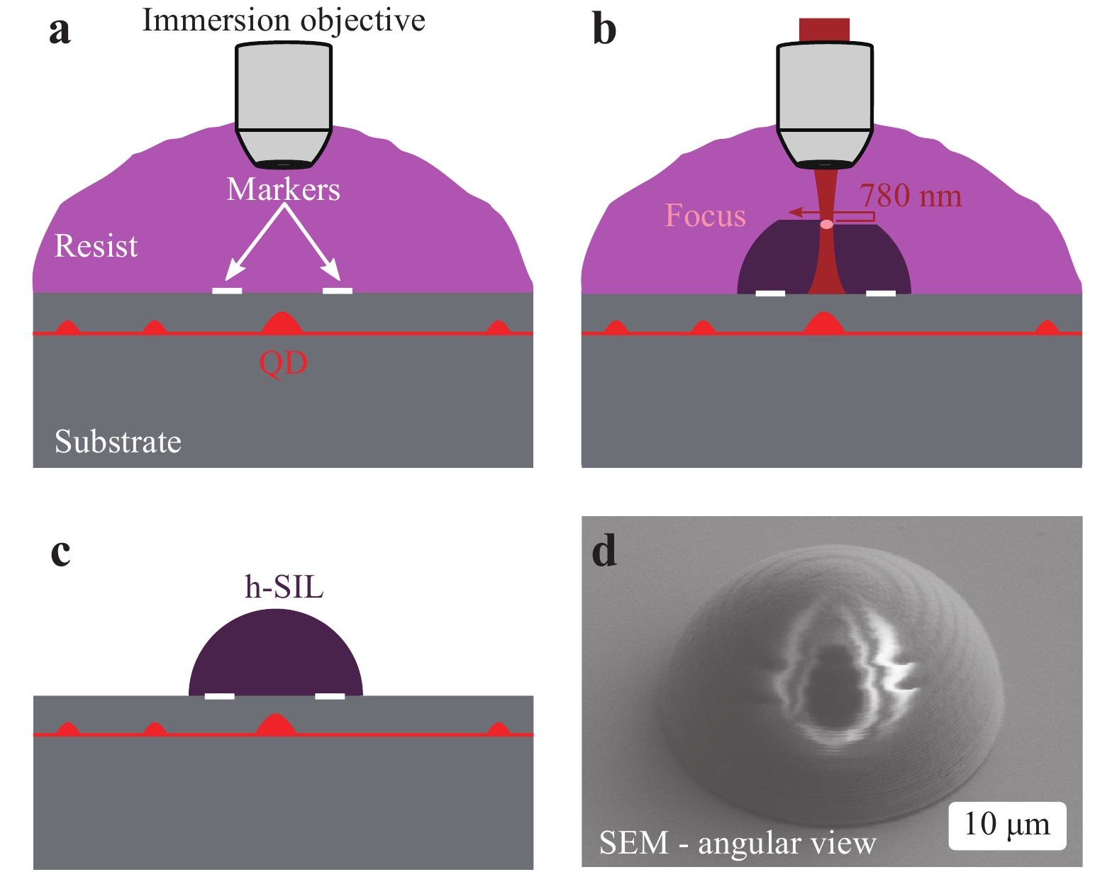
Fig. 27 Schematic process flow of the 3D direct laser writing of an h-SIL.
a Drop coated sample with etched markers. Markers are found via inspection with the depicted immersion microscope objective. b A fs pulsed laser at 780 nm wavelength is focused into the resist. The resist is polymerised only in the laser focus. c Leftover resist is removed using resist developer and isopropanol. d Example SEM image of the finished h-SIL. Because of the non-conductive nature of the resist, charge accumulation is visible.Note added: This paper is based in part on the PhD thesis by Marc Sartison54.
-
We acknowledge the financial support of the German Federal Ministry of Science and Education [Bundesministerium für Bildung und Forschung (BMBF)] via the projects Printoptics, Printfunction, and Q.link.X 16KIS0862, and support via the project EMPIR 17FUN06 SIQUST. This project received funding from Baden-Württemberg-Stiftung via the Opterial project. This project received funding from the EMPIR programme co-financed by the participating states and from the European Union’s Horizon 2020 research and innovation programme. Furthermore, funding was received from the European Research Council (ERC) via the projects AdG ComplexPlas and PoC 3D PrintedOptics. It was also funded by the Deutsche Forschungsgemeinschaft (DFG) via the projects SPP1839, SPP1929, GRK2642, as well as the Center for Integrated Quantum Science and Technology (IQST).
3D printed micro-optics for quantum technology: Optimised coupling of single quantum dot emission into a single-mode fibre
-
Marc Sartison1, ,
 ,
, -
Ksenia Weber2, ,
,
-
Simon Thiele3, ,
,
-
Lucas Bremer4, ,
,
-
Sarah Fischbach4, ,
,
-
Thomas Herzog1, ,
,
-
Sascha Kolatschek1, ,
,
-
Michael Jetter1,
,
-
Stephan Reitzenstein4, ,
,
-
Alois Herkommer3, ,
,
-
Peter Michler1, *, ,
,
-
Simone Luca Portalupi1, ,
,
-
Harald Giessen2, *, ,
- Light: Advanced Manufacturing 2, Article number: 6 (2021)
- Received: 06 July 2020
- Revised: 15 January 2021
- Accepted: 18 January 2021 Published online: 31 March 2021
doi: https://doi.org/10.37188/lam.2021.006
Abstract: Future quantum technology relies crucially on building quantum networks with high fidelity. To achieve this challenging goal, it is of utmost importance to connect individual quantum systems such that their emitted single photons overlap with the highest possible degree of coherence. This requires perfect mode overlap of the emitted light from different emitters, which necessitates the use of single-mode fibres. Here, we present an advanced manufacturing approach to accomplish this task. We combined 3D printed complex micro-optics, such as hemispherical and Weierstrass solid immersion lenses, as well as total internal reflection solid immersion lenses, on top of individual indium arsenide quantum dots with 3D printed optics on single-mode fibres and compared their key features. We observed a systematic increase in the collection efficiency under variations of the lens geometry from roughly 2 for hemispheric solid immersion lenses up to a maximum of greater than 9 for the total internal reflection geometry. Furthermore, the temperature-induced stress was estimated for these particular lens dimensions and results to be approximately 5 meV. Interestingly, the use of solid immersion lenses further increased the localisation accuracy of the emitters to less than 1 nm when acquiring micro-photoluminescence maps. Furthermore, we show that the single-photon character of the source is preserved after device fabrication, reaching a
Research Summary
Quantum technology: 3D printed fibre-based quantum light source
Making quantum networks a reality relies crucially on building efficient optical fibre-based quantum light sources. Here, Harald Giessen and Peter Michler from the University of Stuttgart in Germany and colleagues present an advanced manufacturing approach to accomplish this task. Complex micrometre-sized optics were 3D printed on top of individual indium arsenide quantum dots to enhance their single-photon extraction efficiency. Different lens geometries were systematically investigated to optimise the required optical design and a significant increase in light extraction was achieved. Furthermore, a 3D printed fibre chuck was used to precisely position an optical fibre, equipped with another 3D printed in-coupling lens, onto such a quantum dot. This compact on-chip solution enables high coupling efficiency into a single-mode fibre with high-rate single-photon emission.


Rights and permissions
Open Access This article is licensed under a Creative Commons Attribution 4.0 International License, which permits use, sharing, adaptation, distribution and reproduction in any medium or format, as long as you give appropriate credit to the original author(s) and the source, provide a link to the Creative Commons license, and indicate if changes were made. The images or other third party material in this article are included in the article′s Creative Commons license, unless indicated otherwise in a credit line to the material. If material is not included in the article′s Creative Commons license and your intended use is not permitted by statutory regulation or exceeds the permitted use, you will need to obtain permission directly from the copyright holder. To view a copy of this license, visit http://creativecommons.org/licenses/by/4.0/.

 DownLoad: