


-
The optical state of a material affects not only its visual appearance but also its possible applications. For example, maximizing optical absorption enables sensing, photodetection, steam generation, and the enhancement of solar cell efficiencies and printing ink darkness1–4. In contrast, maximizing reflection is essential for optical mirrors, cavities, or diffractive elements5–8, whereas high transmission is required for see-through applications such as smart windows or displays9–14. Applications may additionally demand switching from one optical state to another, for example, from diffuse reflection to strong absorption, as in most printing, sensing, or data storage applications15,16.
Here, we present a highly absorbing three-layer system that can switch from black to metallic appearance with high reflection and then to a fully transparent state. This multi-state switching is realized by first manufacturing a highly absorbing three-layer system and then modifying it by pulsed laser exposure. While engineering optical absorption and reflectance have been—and still are—extensively researched, this is possibly the first demonstration of the realization of a transparent state from an initially highly absorbing state.
A metal–insulator–metal (MIM) system is a class of structures maximizing absorption in the visible spectrum (VIS)17–21. It typically consists of a metallic base (mirror layer), dielectric spacer, and at least partially metallic top layers. The partially transparent and absorbing metallic top layer can be realized by various approaches, including lithography, to create a periodic pattern. This usually results in a rather narrow absorption band, which is detrimental to many applications1,22,23. However, this absorption band can be broadened through smart optimization methodologies, often at the cost of the maximum achievable absorption17. Another strategy to achieve broadband and near-perfect absorption is the use of a nanocomposite top layer consisting of metal nanoparticles embedded in a dielectric host material21. One possible way to manufacture this nanocomposite layer experimentally is by coevaporation18. Alternatively, laser-induced dewetting of an initially homogenous metal film24 can be used. The realization that it is possible to transform a homogenous metal film into nanoparticles inspired this work. Another important influence was the work of Li et al., who showed that near-perfect absorption is achievable for three-layer systems with a homogenous chromium top layer25.
The advantage of nanocomposite material layers is that their complex refractive index can be easily tuned by varying the metal nanoparticle filling fraction. This is advantageous when the MIM is encapsulated in a high-refractive index material26. In contrast, for surrounding media with low refractive indices, such as air or glass, near-perfect absorption can be achieved using homogenous chromium layers25. Another possibility is to use platinum, which can achieve an optical performance comparable to that of chromium, has a high melting temperature, and does not oxidize; it is often the metal of choice for thermal photovoltaic applications4. Here, we focus on using chromium as it is more economical than gold nanoparticle composites or platinum while providing high absorption in the VIS.
The abovementioned systems are useful in applications where static functionality is important, that is, where the optical properties need to be constant over time, for example, in solar panels. In this work, we focused on applications that require a modification of the optical properties, for example, printing, thus requiring the local modification of the optical appearance. One possible method for changing the optical appearance of homogenous layers is through pulsed laser processing. This approach has been demonstrated by several researchers for single-layer systems. Zywietz et al. showed that silicon spheres can be deposited locally from a homogenous donor silicon layer by focused femtosecond laser pulses27. Their sizes could be controlled, affecting the color produced by their strong electric and magnetic dipole resonances, thus enabling printing in the submicron range. Mao et al. focused on a green continuous wave laser with a high numerical aperture objective to locally create gold nanoparticles from a continuous 12 nm thick gold film28. At the focal spot, the gold film is liquefied and forms nanoparticles that exhibit plasmonic resonances with a colorful optical response different from that of the original gold film. Microscopy revealed that this method can be used to print legible text with a height of a single micron. Guay et al. proved that the color of silver coin surfaces can be directly modified with large topography variations by varying the laser fluences of a nanosecond pulsed laser29. They used a single and multipulse strategy to create vivid colors and observed that multiple pulses in burst mode can broaden the achievable color gamut. In 2019, Odintsova et al. demonstrated similar results by modifying polished bulk substrates for jewelry by varying the intensity and number of nanosecond laser pulses30.
The previous studies showed that single-layer modification works for a plurality of laser sources and metal combinations and can also alter the top layer of multilayer systems9,31–33 or to switch from no transparency to full transparency by ablating a single metal layer34. However, to the best of our knowledge, research has so far focused on switching the local appearance of areas by modifying colorful or metallic surfaces in a binary manner, that is, switching from one reflective/transparent state to another. A noteworthy exception is the gradual modification of either transparency35–37 or reflection38 of high-energy beam-sensitive (HEBS) glasses. These special types of HEBS glasses can be laser-modified with high spatial resolution and applied to grayscale lithography because of the fine tuning of either reflection or transmission with up to 256 discrete levels38.
Here, we aimed to modify a three-layer MIM system that is to transform its initially black state gradually to a plurality of reflection and transmission states. These states included metallic or mirror-like, transparent, semitransparent, and matt-like states. This plurality of achievable states can enable applications in data storage15,16, multi-state printing such as QR codes39, and fabrication of diffractive optical elements that can simultaneously alter amplitude and phase35,40. Any application that demands the realization of multiple states can benefit from this multi-state switching, but we restricted ourselves to a proof-of-principle for multi-state printing and demonstrated a large-area three-dimensional (3D) art image. Note that the printing strategy used here transforms the metallic parts of the MIM system rather than drying and/or applying an ink.
-
The MIM system for all the experiments described below is a three-layer stack of homogenous materials: Cr, MgF2, and Al (Fig. 1a). All three layers are directly vacuum-coated on transparent substrates but can also be applied indirectly via a hot stamping foil. The MIM system was embedded in air and absorbed almost 100% of the incoming light in the VIS based on a lossy Fabry–Perot interference effect. Typically, a Fabry–Perot layer stack consists of a partially transparent absorber, transparent dielectric spacer, and opaque reflector layers41. However, our system initially appeared black due to an exceptionally thin magnesium fluoride MgF2 spacer layer, in the thickness range of 50–70 nm (Fig. 1). Larger thicknesses would lead to the well-known Fabry–Perot reflection peaks in the VIS, which create a colorful appearance41. This effect has been used for more than two decades for the industrial creation of color-changing inks for banknotes42. Embedding the MIM system in a polymer would lead to lower absorption, but the system could be optimized to attain a similar performance to the system embedded in air.
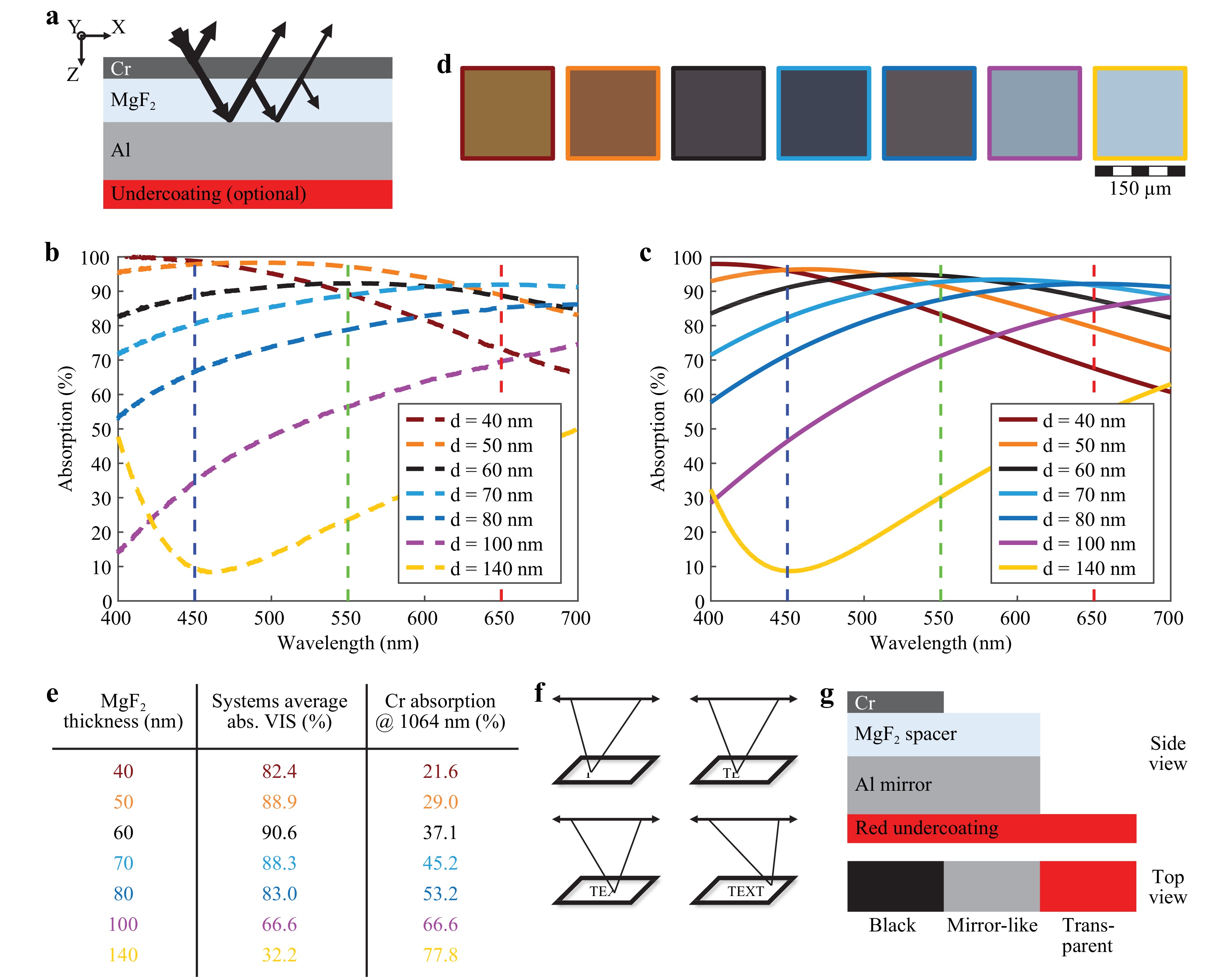
Fig. 1 Simulation and experimental results for three-layer absorbing systems.
a Simulation layout with top semitransparent chromium layer, central dielectric MgF2 spacer layer, bottom aluminum mirror layer, and an optional red undercoating. b, c Measured (dashed lines) and simulated (solid lines) absorption spectra for varying MgF2 thicknesses d and a 9 nm thick top chromium layer. d Microscopic images of the 7 samples shown in panel b, where the edge of each image is highlighted in the color of the corresponding spectra. e Simulated average absorption values of the three-layer system in the VIS and absorption of the chromium layer only at the lasing wavelength λ = 1064 nm. f Illustration of the pointwise raster scanning of the laser focal spot to modify the sample state locally. g Modified three-layer system with partially removed chromium and aluminum layers to create a mirror or transparent state.In addition to the very thin spacer layer, a highly reflective bottom layer is required for realizing high absorption. The reflective layer should be optically thick with negligible transparency (< 1%) to eliminate the influence of the substrate on the optical absorption of the system26. We chose aluminum as the mirror layer material because of its high reflectivity and low cost, which makes the system compatible for mass production. Any aluminum layer > 30 nm thick fulfils the criterion for optical thickness and results in identical optical absorption of the three-layer stack. However, the chosen thickness influences the process window, as will be shown later using four different thickness values: 50, 100, 200, and 400 nm.
The top chromium layer must be partially transparent such that the incoming light is partially transmitted, reflected, and absorbed. The transmitted fraction is reflected at the bottom aluminum layer before reaching the top chromium layer, where a fraction of this light is again transmitted, reflected, and absorbed. These multiple reflections and transmissions lead to a multibeam interference phenomenon (Fig. 1a), resulting in nearly perfect destructive interference over the entire VIS for thin dielectric spacer layers. This requires that the intensity and phase of these multiple beams match, as described in detail in Ref. 43. The optimum chromium layer transmission for high absorption is in the range of 50–70%, corresponding to a thickness in the range of 6–12 nm (Figure S1), which reduces reflections and thus weakens interference, whereas thicker layers prevent multibeam interference owing to their low transmission (Figure S2). Thus, the reflectance spectra in the latter case were dominated by the reflectivity of the chromium layer.
Based on the initial experimental observations, we chose a chromium layer thickness of 9 nm for the MIM system and varied the MgF2 spacer layer thickness experimentally between 40 and 140 nm. The measured absorption spectra in Fig. 1b show that absorption in the VIS is maximized for 50–70 nm thick MgF2 layers. The measured spectra in Fig. 1b agree extremely well with the simulated spectra using Lumerical FDTD, as shown in Fig. 1c44. This good agreement is a consequence of the very smooth multilayer system, as confirmed by AFM measurements (Sq < 2 nm) after evaporation of all three layers (see FigureS3), matching the ideally flat system in the simulations. The FDTD simulations also reveal that almost all visible light is absorbed within the top chromium layer for thicknesses up to 80 nm (see Figure S4). Optical microscopy images of the fabricated samples with different MgF2 spacer layers are shown in Fig. 1d, where each image is framed with the color corresponding to the spectrum in Fig. 1b and Fig. 1c. These images are taken with a 10 × magnifying objective (NA 0.3) and highlight the very different visual appearance of each sample as a function of the MgF2 spacer thickness: the samples with the two thinnest MgF2 spacer layers (40 and 50 nm) appear visually dark brown metallic; the optimal 60 nm thick sample with maximum absorption in the VIS appears nearly perfectly black; the 70 nm thick sample looks metallic dark gray and the 80 nm one gray, whereas the thickest samples (100 and 140 nm thick MgF2 layers) appear metallic light blue. The observed microscopic colors agree very well with a visual inspection because the color is relatively independent of viewing and illumination angle as well as polarization because of the low thickness of the MgF2 spacer layers (see Figure S5). The modest dependency of the system on these observation parameters is confirmed by Figure S6 for observation angles up to 45°, which is sufficient for common low NA observation. When the highest absorption and lowest change are important for an application, s-polarized light should be used for illumination.
The color code of the image frames is also used in the table in Fig. 1e, where the average simulated absorption across the VIS is summarized for all samples, together with the absorption at a wavelength λ of 1064 nm, which is important for the subsequent laser printing process. The simulated average absorption of 90.6% across the VIS for the 60 nm MgF2 spacer layer thickness confirmed the visual and microscopic observation of the blackest appearance. For all remaining experiments, we use a 60 nm thick MgF2 spacer layer, which produces the strongest absorption.
The black state can be switched locally to a reflective or transmissive state by focusing a nanosecond pulsed laser beam on the three-layer stack. Larger areas can be modified by scanning the focal spot across the sample, as shown in Fig. 1f, where the black state is locally modified at the focal spot by a single laser pulse. Between pulses, the focal spot moves to a new position, where the state can be altered with the same or another pulse energy. By repeating this procedure, one can raster scan the sample and modify its appearance locally within polygons, images, or line elements such as text. By varying the laser pulse energy, one can either remove the chromium layer only or remove both the chromium and the aluminum bottom layer. Fig. 1g shows the cross section of the system (side view) for three different states (from left to right): original system, chromium layer removed, and both metal layers removed. In direct reflection, these states correspond respectively to a black, mirror-like, and transparent appearance, as shown in the top view in Fig. 1g.
By further modifying the density of the laser spots, semireflective states: a mixture of black and high reflectance, or semitransparent states: a mixture of black and transparent states, could be realized. This rasterization produces areas of different transparencies, facilitating the realization of 3D impressions and half-tone images45. We first focus on the three-state realization (black, metallic, or transparent) because it allowed us to determine the process window and describe the underlying physical mechanisms.
The commercial laser marking system (Trumpf TruMark Station 5000) operates at λ = 1064 nm and has a typical pulse duration of 24 ns and an average optical power of 2.2 W at a repetition rate of 8 kHz. As shown in Fig. 1e, at λ = 1064 nm, 37.1% of the incoming light power was absorbed within the chromium layer. Simulations further reveal that this accounts for 88% of the total absorption by the system (see Figure S7); thus, in total, approximately 42% of the laser pulse energy is available for the state modification process (5% is absorbed within the aluminum mirror layer). Laser marking systems operating in the near-infrared at 1064 nm are readily available and are often used for the laser personalization processes of ID documents because the involved materials are transparent at this wavelength, or for other industrial applications46. However, a pulsed laser in the VIS would be even more effective because nearly 100% of the incoming energy would be absorbed (Fig. 1e). However, an absorption of only 33% of the laser pulse energy within the top chromium layer is sufficient to melt it, thus switching the system from black to metallic (mirror-like) appearance.
The laser system at hand is typically used for label engraving on bulk metal parts, and its power had to be attenuated by 87.5% for the results in Fig. 2a, b, resulting in an optical power of 0.275 W and an energy per pulse of 34 µJ. In the following, we consider that these values correspond to 100% laser pulse energy; they are sufficient to melt either only the chromium layer or both the chromium layer and a thin bottom aluminum layer. A low-power pulsed laser could also be used for this task, using a multipulse strategy to achieve similar results, as long as the repetition rate is high enough to prevent significant cooling between successive pulses47,48. This emphasizes that the results presented here can be realized with a variety of laser marking systems, and all graphs use a relative scale to reflect this flexibility. Absolute values will depend on the laser system and the pulses overlap, but the curves and results presented here should be reproducible with many different systems. The optical configuration of the system leads to a laser spot size of 40−50 µm, and for all the results in Fig. 2, the distance between consecutive laser spots was chosen to be 50 µm, such that individual laser spots did not overlap. These and all other rasterization schemes used are schematically visualized in Figure S8.
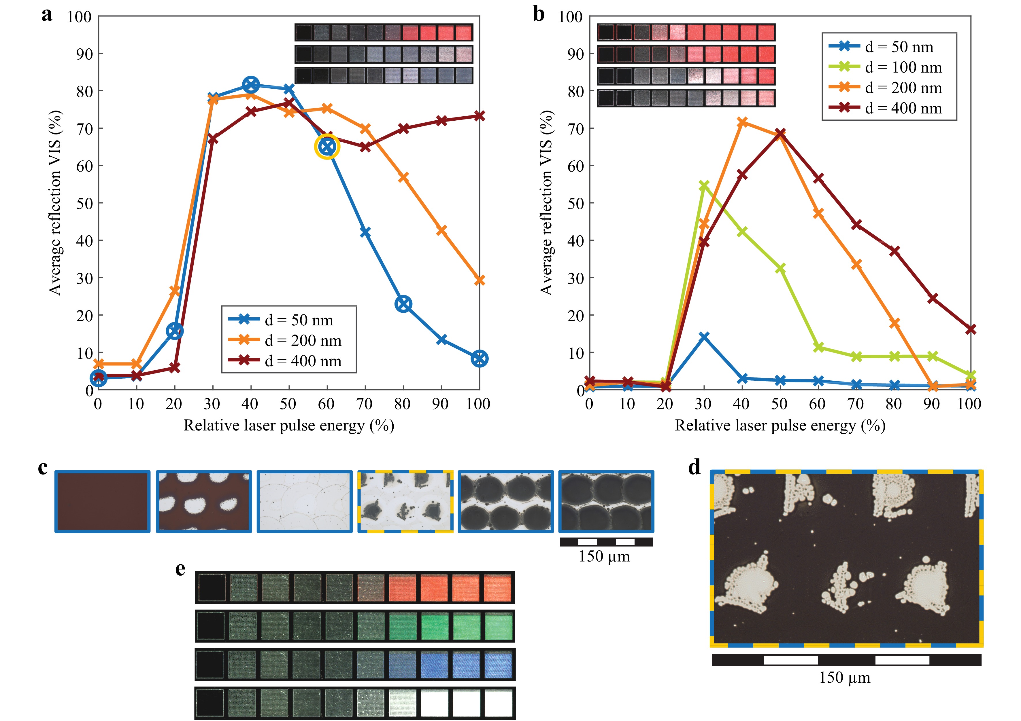
Fig. 2 Gradual state modification of three-layer absorbing systems by pulsed laser processing.
Process windows for three-layer samples manufactured on a, glass or b, PET substrates for different aluminum mirror thicknesses. The insets show photographs of the corresponding sample. c Optical microscopy reflection images for six different laser settings, highlighted by light blue circles in panel a with relative laser pulse energy increasing from 0% to 100% in 20 % steps. d Optical microscopy transmission image of the 60% relative laser pulse energy setting. e Photographs of the test pattern on plain paper and red, green, and blue papers, where the transparent areas reveal the colored undercoating.Fig. 2a shows the relative laser pulse energy versus the average reflection in the VIS. For varying thicknesses of the bottom aluminum layer on glass substrates, the relative laser pulse energy is approximately the same for switching from the initially black state with low average reflection in the VIS to the mirror state with high average reflection, by melting only the top chromium layer. This leads to a drastic increase in the chromium transmission and happens between 20−30% relative laser pulse energy. On the other hand, switching from the metallic to transparent state strongly depends on the aluminum bottom layer thickness: thicker aluminum layers require a higher laser pulse energy and thus a wider range of laser pulse energies can be used to realize the mirror state. Consequently, the process window for the three-transparency-state laser switching is larger for thicker aluminum bottom layers. On further increasing the laser pulse energy, the bottom aluminum and top chromium layers are melted, thus transforming the initially black appearance into a mostly transparent one.
The switching of optical states can also be observed in the inset of Fig. 2a, where the top row is a photograph of the sample with a 50 nm thick aluminum bottom layer, the central row of a 200 nm thick, and the bottom row of a 400 nm thick one. The transparent state was revealed by placing a red paper below the sample. This could also be realized with a thin red dye layer beneath the bottom aluminum layer, as shown in Fig. 1a. Please note that even the thickest 400 nm aluminum layer can be made fully transparent using a higher laser pulse energy (approximately 150%) or by applying several pulses at the same location as previously mentioned and used later.
Another parameter that substantially influences the size of the process window is the choice of the substrate material beneath the three-layer system. The results in Fig. 2a were obtained using 1 mm thick glass substrates, whereas those in Fig. 2b used 19 µm thin polyethylene terephthalate (PET) foils. This change in the substrate material leads to a significant reduction in the process window. The switching from black to mirror state still occurs for relative pulse energies around 20−30%, but the switching from mirror to transparent state occurs at a much lower energy (compare, for example, the orange curves for d = 200 nm in Fig. 2a and 2b). This can also be inferred from the insets in Fig. 2b, which show photographs of the test rows with increasing aluminum layer thicknesses from top to bottom. Even for thick aluminum bottom layers, the laser pulse energy must be precisely controlled to reproducibly switch between the three states, whereas for the 50 nm thick aluminum bottom layer, the mirror state cannot be reached at all. A likely reason for this behavior is that because it has a lower melting temperature, a larger fraction of the top PET substrate melts compared with the glass one49. Furthermore, the boiling temperature of PET is so low that fumes crack the three-layer system at intermediate laser pulse energies, which also increases transmission and consequently lowers reflection. Note that each of the test squares shown in Fig. 2a, b has a side length of 3 mm, and the spectral reflection is measured with a collimated light beam with a diameter of approximately 2.5 mm. Each data point of the average reflection thus corresponds to the mean reflection from approximately 2000 laser processed spots.
The microscope reflection images in Fig. 2c correspond to the blue encircled data points in Fig. 2a. They showed that the initially black state (0% or no laser pulse applied) is partially switched to a mirror-like state at 20% relative laser pulse energy. According to the manufacturer, the laser system used in this work has a significant variation in the laser pulse energy at low powers. Consequently, the successive dots vary in shape and size, as is visible in the second image from the left in Fig. 2c. Thus, this three-layer system can be used to measure the reproducibility of the laser pulses. At a relative laser pulse energy of 40 %, the energy was sufficient to completely melt the top chromium layer. A fraction of the chromium evaporates, but the larger fraction flows to the rim of the laser spot mainly because of thermal gradients, where it solidifies, and it is known that the laser system has and forms small chromium spheres (black dots in Fig. 2c)50. Increasing the relative laser pulse energy further from 60% to 80% and, finally, 100%, results in partial and then full melting of the bottom aluminum layer. The liquefied metal is again redistributed to the rim of the individual laser spots, as can be clearly seen in the rightmost picture, which corresponds to 100% relative laser pulse energy (Fig. 2c). The dark areas in the images for pulse energies between 60% and 100% are in fact transparent areas, as revealed by the transmission microscope image in Fig. 2d, which corresponds to the same location as the 60% relative laser pulse energy image in reflection (see also the encircled yellow data point in Fig. 2a). We observed a contrast reversal between the reflection and transmission images indicating that the area modified by the laser pulse effectively becomes transparent. The insets in Fig. 2a, b are photographs of the samples placed on red paper. Alternatively, one could place the samples on green or blue paper or even blank paper, as shown in Fig. 2e. This illustrates how the transparent state can be used in combination with a suitable undercoating to realize multicolor states. Even a true-color image could be realized by using a background image with red, green, and blue printed pixels and registered laser processing of the MIM system on top.
So far, we have seen that three different optical states can be realized by laser exposure: black, metallic, or transparent. This modification occurs as a localized spot in the material. We next discuss how the rasterization strategy for laser beam spots can create additional states. Fig. 3a shows a 3D art representation of the EPFL logo that required six different states for its realization: black (initial, no switching), metallic, low, medium, and full transparency, as well as a matt state. The front, top, and side faces of the logo have full, medium, and low transparency, respectively. The black lines between the red faces were not modified during laser processing and thus appeared black initially, whereas the background is in the mirror state. At the top left and bottom right, six white EPFL logos were created in a matt state by melting and reflowing of the top chromium layer, as explained later. Below this print, we also created test squares of all five modified states that were used in the logo. To obtain a large process window, we used a glass substrate and an aluminum layer thickness of 400 nm in combination with a 9 nm thick chromium layer and a 60 nm thick MgF2 layer for all experimental results shown in Fig. 3.
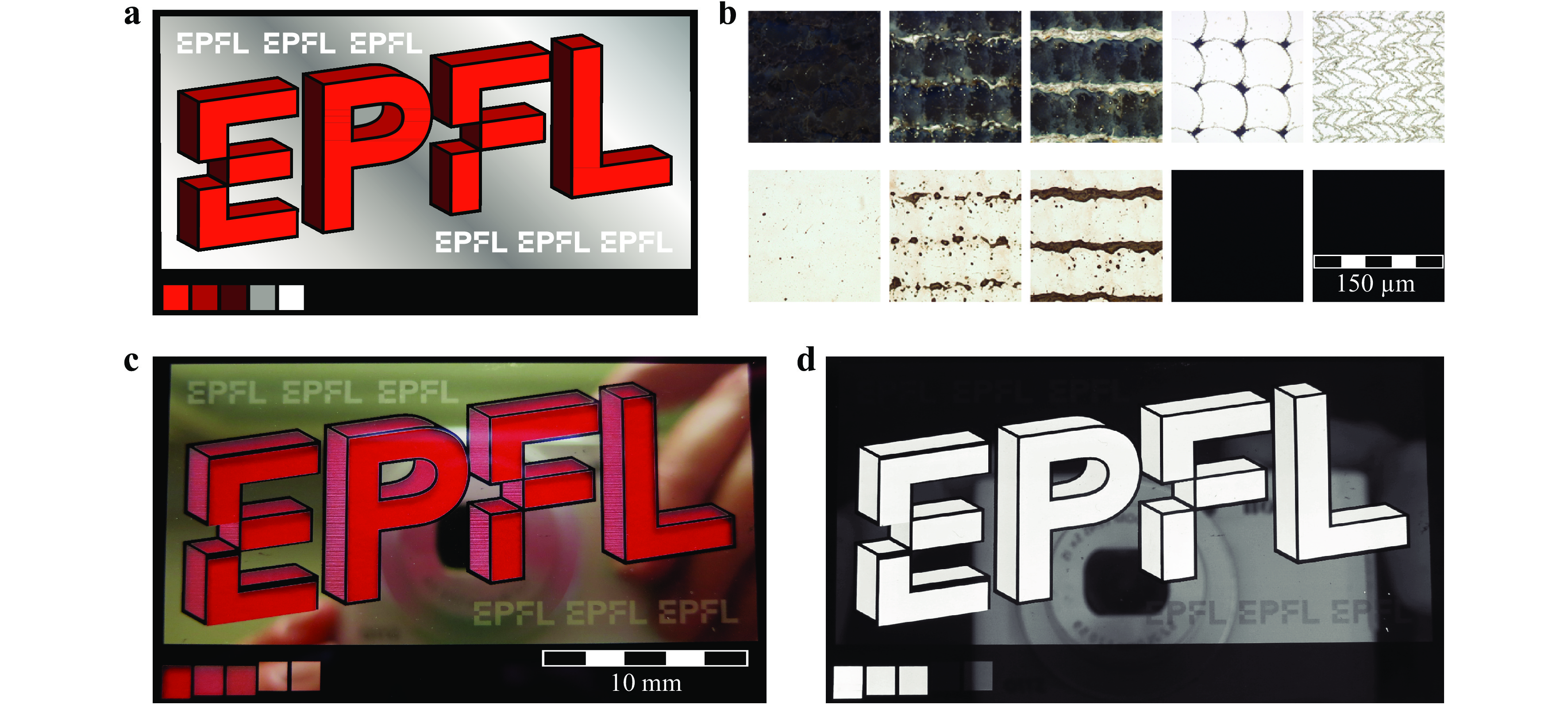
Fig. 3 Demonstration of three-state laser printing by pulsed laser processing.
a 3D artwork used for multi-state laser printing. b Photograph of the laser-printed 3D artwork placed on top of a red paper. c Optical microscopy reflection (top row) and transmission images (bottom row) of the five test patterns used for optimization of the printing parameters for both metallic and (semi) transparent states. d Photograph of the laser-printed 3D artwork illuminated from the back.Fig. 3c shows a photograph of the laser-modified sample placed on the red paper. The scattering matt state for the three 2D EPFL logos at the top and bottom, as well as the differences in transparency for the 3D logo faces are clearly seen. They agree well with the original 3D art design in Fig. 3a. On the bottom left of the picture, the quadratic test patterns for the five different optical states can be seen. These five states were imaged with an optical microscope, as shown in Fig. 3b where the top row corresponds to the reflection images and the bottom row corresponds to the transmission images; each column corresponds to one of the test patterns in Fig. 3c. The three left image columns reveal that these test patterns are mostly transparent and have weak blocking lines in the medium and low transparency states. The red color in reflection is a result of placing the sample on a red sheet of paper, and any other color tone would be possible, as demonstrated in Fig. 2e. The varying transmission grades of these three states can also be observed directly by inspecting the sample in transmission. Fig. 3d shows a photograph of the sample illuminated from the back. Note that the camera is visible in reflection because of the scattering of the transmitted light by the camera’s white front face. The fourth column from the left shows a mirror-like state, where the chromium flowed to the rims of the individual laser spots. This state is also used as a background for 3D art, which is highly reflective, as confirmed by the reflection of the camera. Finally, the rightmost column in Fig. 3b shows microscopic images of the matt state and reveals the pseudoperiodic reflow of the chromium top layer. The last two states (mirror-like and matt) show no transmission, as evidenced by the corresponding optical microscope transmission images (Fig. 3b, bottom row).
All the five optical states were created by varying the laser rasterization strategy, whereas the black state required no laser exposure because it corresponds to the original three-layer system itself. The mirror state was realized as previously described by melting the top chromium layer with a single pulse strategy and 50 µm spacing between consecutive laser spots at an intermediate energy of 29% to reveal the aluminum mirror beneath. Both the semitransparent states were realized by adjusting the raster distance in one direction. Each (semi) transparent area of the 3D art image was rastered line wise, and a 25 µm distance between consecutive spots was used along this horizontal line by reducing the scanning speed to 50% of its original value of 400 mm/s. The distance between successive raster lines in the vertical direction is changed to 60 μm for medium transparency, resulting ideally in 10 μm wide black lines between the 50 μm wide transparent lines. For low transparency, the raster spacing was increased to 70 μm, resulting in 20 μm wide black lines. The fully transparent state was realized with a multipulse strategy by decreasing the line spacing to 25 µm. This produces an overlap of approximately 50% of the individual laser spots in both directions and ensures that the transparency is maximized. The series of white EPFL logos in the 3D artwork in Fig. 3a required an additional matt state corresponding to strong light scattering. This was realized with a slightly lower relative laser pulse energy (27%) than that used for the mirror-like state (29%) but with an even larger spatial overlap of the individual laser spots, that is, 75% overlap along a horizontal line and thus also a multipulse strategy. This caused multiple reflows and solidification of the chromium top layer. The liquefied chromium flowed toward the rim of each laser spot owing to the thermal gradient resulting in a pseudoperiodic pattern with a mean period length of 15 µm, as shown in Fig. 3b top right. The reflow generated a topography that alters the phase of incoming light and ultimately leads to scattering. The periodicity of this pattern is broken mostly because of the limited precision of the laser scanning system. All laser and raster parameters are schematically visualized in Figure S8 and summarized in Supplementary Table 1.
-
In summary, we manufactured three-layer systems that absorb more than 90% of the incident light in the VIS and thus have a black appearance. The measured absorption spectra of the initial black state agreed well with the simulation data. The black appearance was locally modified by focusing a λ = 1064 nm nanosecond pulsed laser to 50-micron sized spots. This allowed us to realize a six-state 3D artwork print with defined areas containing either a black, mirror-like, matt-like, or one of the three transparent states. Transparency was selectively tuned in three different grades by altering the raster strategy of the printing process. Realizing additional transparent states would be straightforward by further altering the rasterization. The influence of the substrate material and metallic bottom layer thickness on the process window of this novel multi-state process was determined and discussed in detail. The experiments were supported by numerical simulations, and the agreement between the two was excellent. We envision that the findings for the multi-state print presented here are readily transferable to other research areas, including the fabrication of novel diffractive optical elements by local modifications of its reflection, transmission, and phase properties.
-
An Avatec ULS3648-USB2 spectrometer in combination with the reflection probe FCR-7UVIR200-2-ME and a broadband light source Thorlabs SLS201/M was used for all spectroscopic measurements. Sample transmission was not measured because the three-layer stack was optically opaque owing to the thick aluminum bottom layer. The measured absorption spectra correspond to 100% − reflection [%].
-
The chromium and aluminum layers were evaporated using a Leybold Heraeus L560 by electron-beam evaporation. For the deposition of aluminum, the chamber was evacuated to a pressure of 3.5 × 10⁻⁵ mbar, and the deposition rate was adjusted to 0.4–0.8 nm/s. Chromium evaporation was performed at a pressure of 3.5 × 10⁻⁵ mbar, and the deposition rate was adjusted to 0.2–0.3 nm/s. The MgF2 spacer layer was applied by thermal evaporation with a tectra GmbH Mini-Coater at a pressure of 2 × 10⁻⁵ mbar and a deposition rate in the range 0.8–1.2 nm/s.
-
Spectral simulations were performed using Lumerical FDTD44. A linearly polarized broadband source from λ = 350 to 1100 nm was used to illuminate the three-layer system. The simulation volume was set to 10 nm × 10 nm × 2000 nm with a conformal meshing of variant 1 with an accuracy of 5. The mesh in and close to the chromium and MgF2 layers was overwritten to a maximum size of 2 nm × 2 nm × 0.25 nm, mainly to ensure accurate resemblance of the layer dimensions in the axial direction. Bloch-type periodic boundary conditions were selected laterally and perfectly matching layers with 32 layers in the z-direction. Power detectors were placed at appropriate positions in accordance with the recommendations of Lumerical to achieve the highest possible accuracy in reflection and absorption detection. The material data for aluminum, chromium, and MgF2 are based on literature values51−53.
-
We gratefully acknowledge the valuable discussions with Rossen Todorov about the accuracy of modeling of thin chromium films using appropriate refractive index data measured for thin films.
Engineering multi-state transparency on demand
- Light: Advanced Manufacturing 2, Article number: 26 (2021)
- Received: 15 September 2021
- Revised: 19 October 2021
- Accepted: 27 October 2021 Published online: 13 December 2021
doi: https://doi.org/10.37188/lam.2021.026
Abstract: Materials are, in general, either transparent or not. In principle, it is impossible to switch a material from a reflective optical state to a fully transparent one. Transparency has received relatively less research attention compared to other optical properties such as absorption, research on which have successfully produced perfect blacks, that is, highly absorbing materials. The ability to change optical transparency, especially locally and on demand, can enable several applications. Here, we present an absorbing three-layer system whose transparency can be altered by pulsed laser processing to realize different states, ranging from full transparency to mirror, black, and combinations thereof. An initially black surface can be made highly reflective or transparent by changing the laser pulse energy. The corresponding process window, including the influence of the substrate material, was investigated in detail.
Research Summary
Optical appearance: Laser switching from black to full transparency
Engineering the transparency of a material that is originally black enables myriad of applications, including printing, photovoltaics, sensing, reconfigurable surfaces, customizable security solutions, diffractive optical elements, and data storage. Sebastian Mader and Olivier J.F. Martin from the Swiss Federal Institute of Technology in Lausanne have discovered means of altering locally and on demand the appearance of an absorbing three-layer system by pulsed laser processing. They realized different optical states, ranging from absorbing black to highly reflective, fully transparent, or even combinations thereof. An initially black surface becomes reflective or transparent by simply changing the used laser pulse energy. These findings are applied to realize high-resolution, multi-state printings of a 3D artwork.
Rights and permissions
Open Access This article is licensed under a Creative Commons Attribution 4.0 International License, which permits use, sharing, adaptation, distribution and reproduction in any medium or format, as long as you give appropriate credit to the original author(s) and the source, provide a link to the Creative Commons license, and indicate if changes were made. The images or other third party material in this article are included in the article′s Creative Commons license, unless indicated otherwise in a credit line to the material. If material is not included in the article′s Creative Commons license and your intended use is not permitted by statutory regulation or exceeds the permitted use, you will need to obtain permission directly from the copyright holder. To view a copy of this license, visit http://creativecommons.org/licenses/by/4.0/.

 DownLoad: