


-
Measurement technology is crucial for manufacturing. Terahertz (THz) electromagnetic waves1, which lie between the microwave and infrared (IR) spectral ranges, have great potential in manufacturing processes for the characterization of material and electronic properties. Compared with visible/IR radiation, THz electromagnetic waves are less affected by scattering owing to their long wavelengths and can deeply penetrate materials, which is beneficial for imaging2−5 and spectroscopy6−9 applications. Furthermore, THz electromagnetic waves have small photon energies (1 THz = ~4 meV); therefore, they are non-ionizing and biologically safe. Among their advantages, we emphasize that THz photon energies match various energy/frequency scales (quantization energies, plasma frequencies, etc.) in nanomaterials, such as quantum dots (QDs)10, 11, carbon nanotubes (CNTs)12, 13, and nanowires (NWs)14, 15, allowing THz electromagnetic waves can interact with various types of electronic excitations. Furthermore, molecular vibration frequencies, such as center-of-mass motions, bending modes, and rotational modes, lie in the THz range. Such features make THz spectroscopy an attractive and powerful tool for characterizing the properties of various types of nanomaterials and molecules. These features of THz spectroscopy are complementary to IR spectroscopy, which is often used to study interatomic vibrations in molecules.
However, the long wavelengths of THz electromagnetic waves pose challenges for performing spectroscopy at the nanometer (nm) scale. The typical wavelengths of THz waves lie between 3 mm and 10 μm (corresponding to 0.1-30 THz). Because of the diffraction limit, it is difficult to focus THz electromagnetic waves on nm-scale samples. Therefore, conventional THz measurements using free-space optics, such as THz time-domain spectroscopy8, 16 and Fourier transform IR spectroscopy10, 11, have mainly been performed on samples several millimeters in size2, as schematically shown in Fig. 1a. This is acceptable for the measurement of large samples, such as semiconductor wafers and biological tissues16−19. However, with the progress in nanotechnology, the demand for measuring the properties of single nanostructures is increasing. For instance, to realize advanced quantum nanodevices for information processing, the electronic structures and dynamic properties of single quantum nanostructures must be understood, and advanced pharmaceutical applications require the characterization of molecules at the individual level. Therefore, while THz spectroscopy at the nm scale is becoming increasingly necessary, it is far beyond the capability of conventional THz spectroscopy techniques.
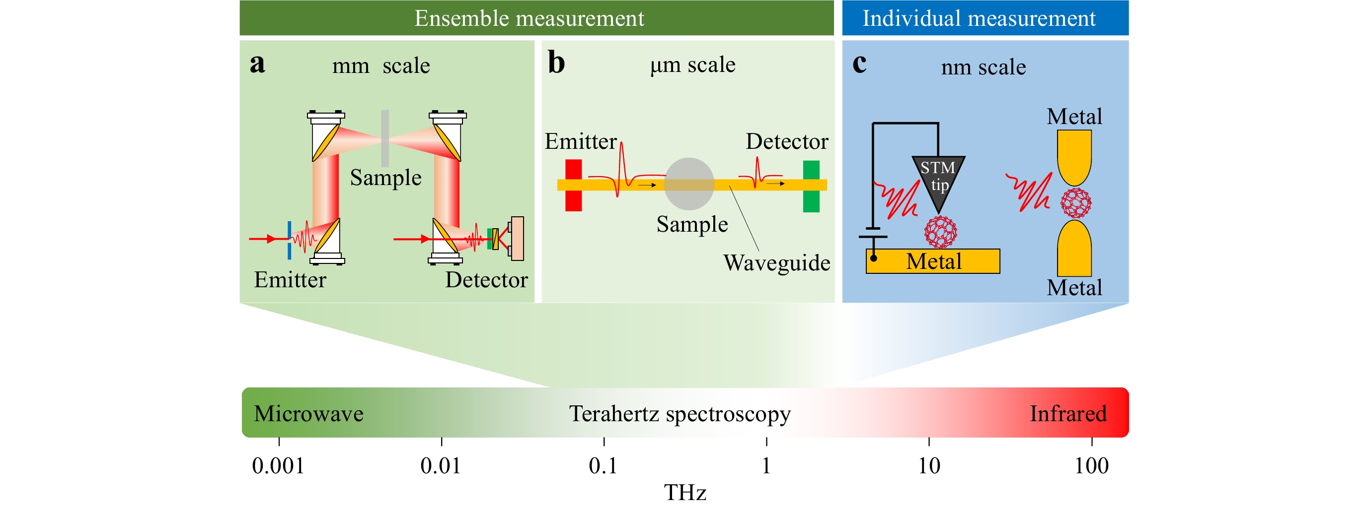
Fig. 1
Schematic of the development of THz spectroscopy from a the millimeter scale to the b micrometer and c nanometer scales.Over the last decade, several groups have attempted to overcome the diffraction limit by building on-chip systems with integrated THz sources, waveguides, and detectors20−25. Compared with conventional free-space measurement systems, on-chip THz spectroscopy systems can reduce the sample size to the subwavelength range, and the necessary sample volume is significantly reduced to approximately the cubic micrometer level, as schematically shown in Fig. 1b. Furthermore, an on-chip THz spectroscopy system can be integrated with microfluidic structures26−28. THz metamaterial resonators29−32 can also be introduced to compress the mode volume and improve the signal-to-noise ratio. Femtomolar-order sensitivity has been reported29, 30 for the detection of large biomolecules, such as deoxyribonucleic acid (DNA). However, the sensitivities of such systems remain insufficient for measuring the THz spectra of single nanostructures. To realize nm-scale THz spectroscopy, new measurement schemes that are different from simple transmission or reflection measurements are required.
Nanoscale THz spectroscopy is very challenging because it requires a new scheme not only for focusing THz electromagnetic waves onto nm-scale regions but also for high-sensitivity detection of the extremely weak absorption by nm-scale systems. Three types of nanoscale THz spectroscopy techniques have been reported, namely, THz scattering-type scanning near-field optical microscopy (THz s-SNOM)33−38, THz scanning tunneling microscopy (THz-STM)39−48, and THz single-electron tunneling spectroscopy (THz-SETS)49−54. In these measurements, the THz electromagnetic wave is focused onto nm-scale systems using either a scanning probe or nanogap electrodes, as schematically shown in Fig. 1c. By detecting THz electromagnetic waves scattered by a measurement target or by measuring the photocurrent induced by THz photoexcitation in the sample, the THz response of single quantum nanostructures can be detected. By providing a key scientific basis for understanding the physics and the application of nanostructures and single molecules, nm-scale THz spectroscopy has great potential in the fields of nanoscience and technology.
This paper aims to provide a comprehensive review of the recent progress in nm-scale THz spectroscopy using THz-SETS. In Section 1, we provide a general introduction to conventional and nm-scale THz spectroscopy. Section 2 describes the principles of the three types of nm-scale THz spectroscopy, that is, THz s-SNOM, THz-STM, and THz-SETS, and compares their characteristics. In Section 3, we provide a detailed description of THz-SETS and discuss the crucial aspects for achieving ultrahigh-sensitivity measurements. Section 4 presents examples of nm-scale THz dynamics revealed by THz-SETS to demonstrate the effectiveness of this technique. Finally, in Section 5, we conclude this review and provide an outlook on how nm-scale THz spectroscopy will advance the cutting edge of THz technologies and related nanotechnologies.
-
To realize nm-scale THz spectroscopy, THz electromagnetic waves must be tightly focused onto nm-scale systems, and extremely weak absorption must be detected with high sensitivity. Depending on the method used to detect the extremely weak THz absorption, nm-scale THz spectroscopy techniques can be classified into the following three categories: (i) THz s-SNOM, (ii) THz-STM, and (iii) THz-SETS. Table 1 shows a comparison of the three methods, and their characteristics are described below.
THz s-SNOM THz-STM THz-SETS Imaging yes yes no Gating at the nm scale difficult difficult easy Requires powerful THz source yes yes no Signals scattered power photocurrent photocurrent Table 1. Comparison of THz s-SNOM, THz-STM, and THz-SETS.
-
THz s-SNOM33−38 provided a breakthrough in the diffraction limit in free-space optics and enabled the measurement of nm-scale samples, as shown in Fig. 2a. A metal-coated atomic force microscopy (AFM) tip is used as an antenna to concentrate incident THz radiation to a nm-scale near-field spot at the tip apex. When the tip is close to the sample surface, the near-field interaction between the tip and sample modifies the tip-scattered THz field, which depends on the local dielectric properties of the sample. By collecting the scattered THz light in the far field, THz spectroscopy and imaging can be achieved at the nm scale.
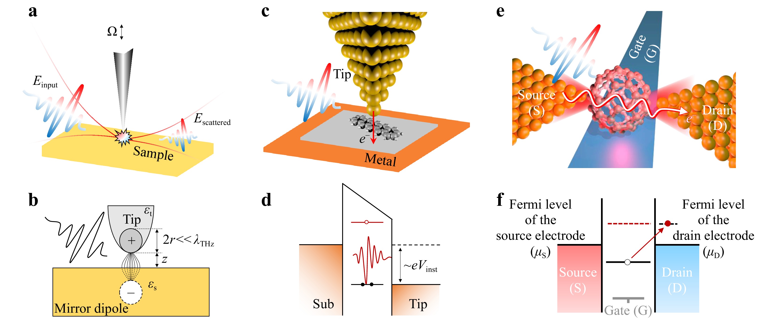
Fig. 2
a Schematic of THz s-SNOM. b Model of the near-field interaction in THz s-SNOM. The AFM probe tip is assumed to be a polarizable sphere with dielectric constant εt. A point dipole can be used to replace the probe tip, which allows the prediction of the dependence of the scattered THz wave on the distance z between the tip and sample and on the complex dielectric constant εs of the sample. c Schematic of THz-STM. d Tunneling process of single molecular orbitals in THz-STM measurements. Vinst is the instantaneous voltage between the tip and substrate induced by THz pulses. e Schematic of THz-SETS. f THz-induced vibron-assisted tunneling in an SMT.The near-field interaction between the tip and sample is the key to the THz s-SNOM technique. The THz s-SNOM system can be regarded as a simple model that includes the tip and the sample, as shown in Fig. 2b. The effective polarizability of the coupled tip–sample system (αeff) can be expressed by the polarizability of the tip (α) and the dielectric surface response function of the sample (β)55.
$$ {\alpha }_{\mathrm{e}\mathrm{f}\mathrm{f}}=\frac{\alpha (1 +\beta )}{1 -\alpha \beta /\left(16\pi {\left(r+z\right)}^{3}\right)} $$ (1) $$ \alpha = 4\pi {r}^{3}\frac{{\varepsilon }_{t}- 1}{{\varepsilon }_{t}+ 2} $$ (2) $$ \beta =\frac{{\varepsilon }_{s}- 1}{{\varepsilon }_{s}+ 1} $$ (3) where r is the radius of the assumed polarizable sphere at the tip, z represents the distance between the tip and sample, and εt and εs are the dielectric constants of the tip and sample, respectively. Typically, the tip is used in tapping mode, and by detecting the scattered THz signal at the tapping frequency, the weak signal from nm-scale regions can be extracted from the overwhelming background radiation. The THz signal from the sample can be obtained by measuring only the scattered component of the THz field (Es) because Es is proportional to αeffEi (Ei is the incident THz field). Using this technique, THz intersublevel transitions in single QDs have been measured33, 36, 37. However, owing to the very weak backscattered light, a powerful THz radiation source, such as a free electron laser, is required.
-
THz-STM39−48 is another method that uses a nanoprobe. The essential difference from THz s-SNOM is that the signal measured in this method is the tunneling current instead of the scattered light power. Owing to the ultrahigh spatial resolution of STM imaging, nm-scale samples can be well resolved. As shown in Fig. 2c, a nm-scale sample is placed between an atomically sharp tip and a conducting substrate, and pulsed THz radiation is focused onto the sample. To avoid hybridization between the electronic orbitals of the sample and substrate, the substrate surface is sometimes covered by a very thin insulating layer46. When a THz pulse is coupled to the STM tip, it generates an ultrafast voltage transient and forms a THz-induced tunneling photocurrent between the atomically sharp tip and sample, as shown in Fig. 2d. To overcome the large binding energies of electronic orbitals in molecules, strong incident THz fields are typically necessary. Owing to the high sensitivity and high spatial resolution of THz-induced tunneling photocurrent measurements, THz-STM can map the shapes of the highest occupied molecular orbital (HOMO)/lowest unoccupied molecular orbital (LUMO) wavefunctions46.
Extensive THz s-SNOM and THz-STM measurements have been performed to study nanostructures and molecules. For more details, please refer to an excellent recently published review article56.
-
THz-SETS is a simple and powerful nm-scale THz spectroscopy method that was recently developed49−54. THz-SETS is based on a single-electron transistor (SET) geometry, as shown in Fig. 2e. The source and drain electrodes are separated by a gap on the order of sub-nanometer to a few tens of nanometers and focus THz electromagnetic waves onto a nm-scale system captured in the nanogap. Although it lacks imaging capabilities, the great advantage of the SET geometry is that, by using the gate electrode, the electrochemical potential and the charge state in the nanostructures can be precisely tuned, as shown in Fig. 2f. The ability to change the electrochemical potential is particularly important for the study of QDs and molecules, whose electron dynamics are strongly modulated by the electron number. When a QD or single molecule is illuminated by THz radiation, a very small but finite THz-induced photocurrent is generated. Furthermore, excitation spectra associated with intersublevel transitions or molecular vibrations can be obtained.
THz-SETS has an invaluable advantage over the other two methods, as summarized in Table 1. The THz-SETS geometry allows the modulation of the electrostatic potential and the number of conducting electrons in nanostructures by using a gate electrode. Because of this ability to tune the band structure of nanostructures, even very weak THz radiation from a blackbody light source can photoexcite electrons and produce photocurrent signals. Otherwise, intense THz light pulses are required to photoionize nanostructures.
-
In this section, we explain additional details of THz-SETS and demonstrate how it works by introducing examples involving single InAs self-assembled QDs and single molecules.
-
To collect the maximum amount of THz power on a nm-scale sample, a solid immersion lens and metal nanogap electrodes integrated with a THz antenna structure are used, as schematically shown in Fig. 3a. A high-resistivity Si is used to make the hyperhemispherical lens. A THz electromagnetic wave is further focused into the nanogap region owing to the antenna effect of the source–drain electrodes, which greatly enhances the THz field in the nanogap area. Nanogap electrodes with various gap sizes (typically 20−50 nm) are fabricated using standard electron-beam (EB) lithography and subsequent Ti/Au deposition for the measurement of InAs QDs49, 51, 52, InAs quantum dashes (QDHs)50, InAs NWs, and CNTs13, as shown in Fig. 3b−e.
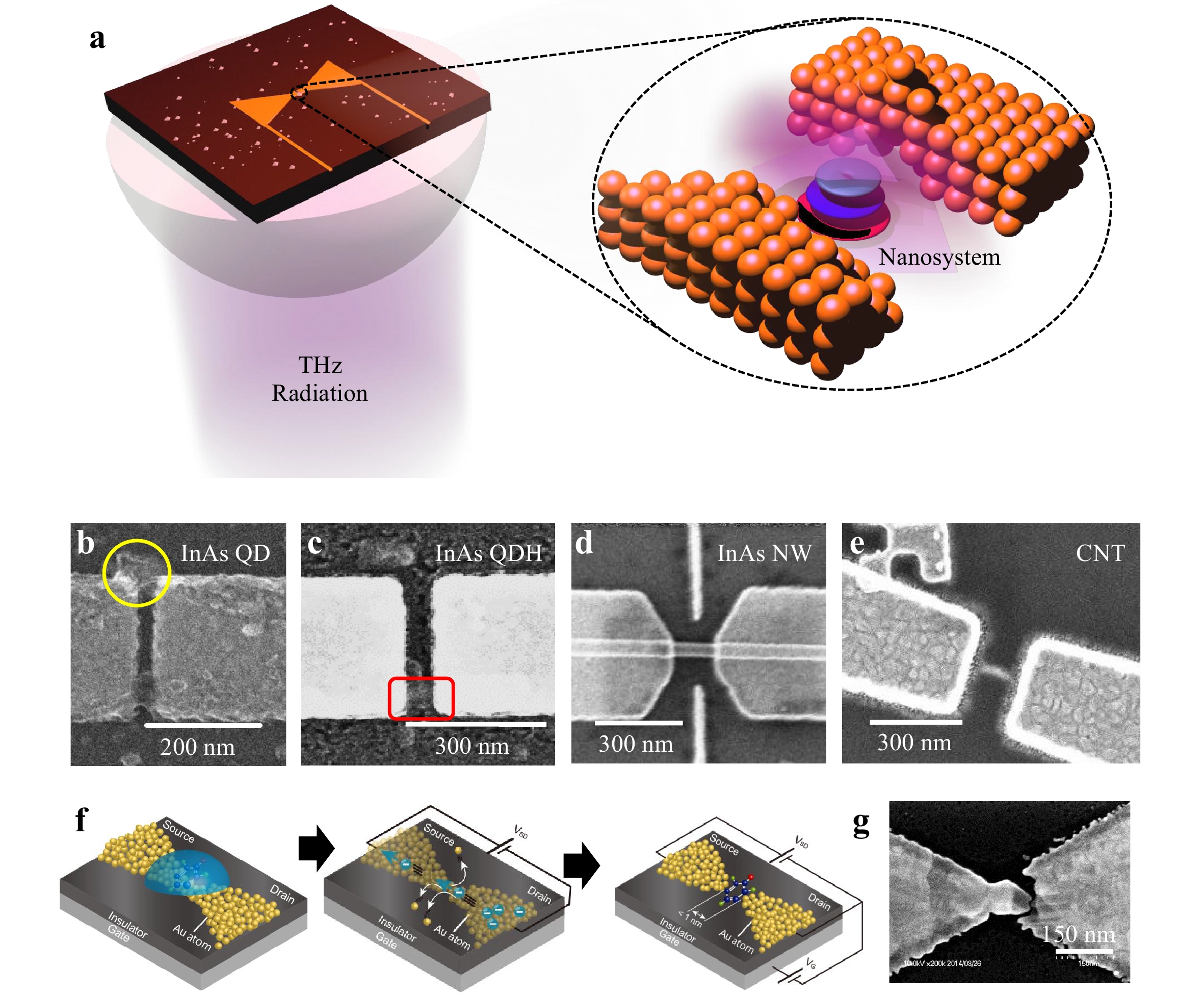
Fig. 3
a Schematic of the THz-SETS measurement setup49. b Scanning electron microscopy (SEM) image of an InAs QD-SET51. c SEM image of an InAs QDH-SET52. d SEM image of an InAs NW-SET. e SEM image of a CNT-SET13. f Schematic of the fabrication process of 1-nm-scale metal nanogaps for capturing a single molecule, including the fabrication of metal nanojunctions, deposition of a molecular solution, and breaking of metal nanojunctions by feedback-controlled EM. g SEM image of the nanojunction region after the EM process53. Images reprinted with the following permissions: a and b from ACS, c from APS, and g from Springer Nature.For measuring systems in deep-nm regions, such as single molecules, the standard top-down nanofabrication process using EB lithography does not work. Instead, a technique called the “electrical break junction” method is used to reproducibly generate sub-nm gaps. The entire process of sub-nm gap fabrication can be separated into two steps. First, a metal nanojunction is fabricated on a substrate using a technique called “shadow evaporation”57. Then, a solution of molecules is deposited on the nanojunction, and the feedback-controlled electromigration (EM) technique58−60 is applied to create a nanogap to capture a single molecule, as schematically shown in Fig. 3f. The electrical break junction process with feedback control enables the reproducible fabrication of sub-nm gaps, as shown in Fig. 3g.
The THz field in the nanogap area is greatly enhanced from its value in free space because the incident THz light is squeezed into the nanogap region owing to the antenna effect. The enhancement factor of the THz field was quantitatively estimated by measuring the strength of the photon-assisted tunneling effect61, 62, reaching values as high as ~105. This enhancement factor can be well explained by the fact that radiation with a wavelength (λ) of ~100 μm is squeezed into a gap (d) of ~1 nm, that is, the enhancement factor is ~λ/d.
-
The enhanced THz electromagnetic field on single QDs or molecules induces photoexcitation. However, reading such signals is not trivial. In QDs and molecules, electronic states are quantized, and only a few conduction electrons can be excited by the THz field. Therefore, the detection of such few-electron absorption by conventional transmission or reflection measurements is extremely difficult. To overcome this problem, nanogap electrodes are used as source/drain electrodes to form a transistor structure for nm-scale systems (QDs, molecules, etc.), and the photocurrent is measured through the transistor. The photocurrent is induced by THz photoexcitation in the QDs or molecules, either by intersublevel transitions or by THz-excited molecular vibrations. This makes the measurement sensitive only to the THz power absorbed by the sensing target. Furthermore, to suppress thermal fluctuations and thermal broadening effects in THz photocurrent measurements, the sample is typically cooled to the temperature of liquid helium (~4.2 K), at which the sample functions as an SET. In the Coulomb blockade region of SETs, the dark current is suppressed, and hence, the noise in the photocurrent measurements is very small; a photocurrent as small as ~10 fA can be detected.
To obtain the photocurrent spectra, Fourier transform spectroscopy or THz autocorrelation measurements with femtosecond laser pulses are used, as shown in Fig. 4a, b. The differences between the two systems are as follows. The former employs a blackbody radiation source that provides weak, broadband, and continuous THz electromagnetic waves. The latter delivers THz pulses whose intensity has a peak mainly at low frequencies (~1 THz for THz photoconductive antennas and several THz for semiconductor surface emitters), as shown in Fig. 4c. Although the THz light sources are different, both methods measure THz autocorrelation signals using a Michelson interferometer. The photocurrent through the SET structure is measured as a function of the position of the moving mirror. Then, THz spectra are obtained by calculating the Fourier spectra of the measured autocorrelation waveforms of the photocurrent, which contain information on THz excitation in nm-scale systems.
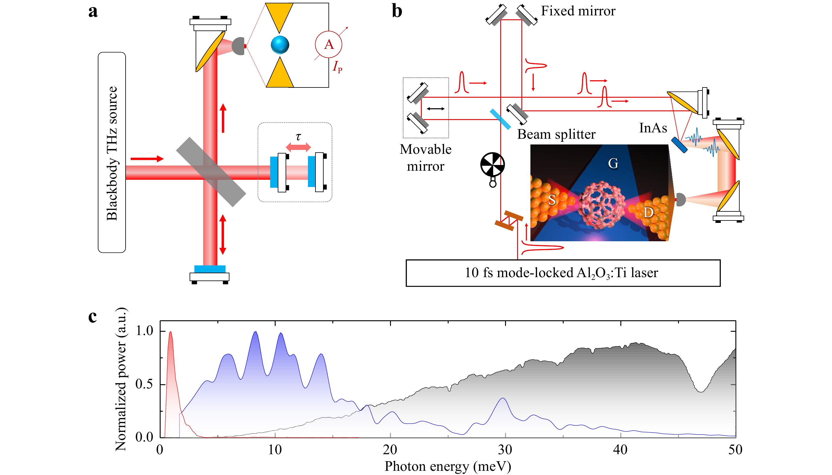
Fig. 4
a Schematic of Fourier transform IR spectrometry (FTIR) for realizing THz-SETS. b Schematic of THz autocorrelation measurements with a femtosecond laser. Femtosecond laser pulses are split into two beams and focused on an InAs wafer as a THz emitter53. c Normalized THz spectrum of the blackbody light source (black), THz spectrum generated from an InAs surface excited by a 10 fs Al2O3:Ti laser (blue), and THz spectrum generated by a photoconductive antenna excited by a 100 fs Al2O3:Ti laser (red). Images reprinted with the following permission: b from Springer Nature. -
In this section, we present examples of THz signals in two types of nanostructures: self-assembled InAs QDs and fullerene molecules. These examples demonstrate the effectiveness of THz-SETS as a powerful tool for exploring nm-scale THz physics.
-
Self-assembled InAs QDs are a promising material system for realizing quantum effect devices, such as QD lasers and single-photon sources63. The key feature of self-assembled QDs is their zero-dimensional discrete energy levels. The realization of quantum effect devices requires precise information on the energy-level structures in QDs. THz intersublevel transitions in single InAs QDs were studied using THz-SETS. Taking advantage of THz spectra with narrow linewidths and high signal-to-noise ratios, the transition dynamics and electron-electron interactions can be studied at the single- or few-electron level.
Fig. 5a, c show schematic energy band diagrams of a QD-SET, which illustrate the mechanisms of photocurrent generation by THz photoexcitation. In a self-assembled InAs QD, the energy states are quantized owing to three-dimensional confinement. A backgate is used to modulate the electrostatic potential in the QD. When the QD is illuminated by a broadband blackbody light source, an electron from a lower-energy state transitions to a higher-energy state by absorbing a THz photon. Then, the excited electron tunnels into one of the source/drain electrodes, and an electron from one of the electrodes tunnels into the empty lower state. Depending on the position of the electrochemical potential in the QD, the electron tunneling-in and tunneling-out processes can have different sequences, which are called the “N → N − 1” and the “N → N + 1” processes49, as shown in Fig. 5a, c, respectively. Fig. 5b, d show schematics of the photocurrent distributions of the “N → N − 1” and “N → N + 1” processes, respectively. Fig. 5e plots the measured photocurrent with respect to the source–drain voltage (VDS) and gate voltage (VG). Comparing the experimental results and theoretical predictions, the photocurrent distribution shown in Fig. 5e indicates that the induced photocurrent arises from the “N → N + 1” process. Fig. 5f shows the measured photocurrent as a function of the bias voltage (VDS). The photocurrent through the QD-SET is on the order of 1 pA and exhibits a stepwise increase with increasing VDS, which is caused by the discrete nature of the energy states and the Coulomb repulsion in the QD. It should be noted that there is a finite photocurrent even at VDS = 0, indicating that the photocurrent mechanism consists of not only a simple photoconduction effect but also a photovoltaic effect. This photovoltaic effect originates from the inherent asymmetry in the four tunneling rates between the QD and the source/drain electrodes for the ground and excited states13, 51 and may be useful in nanoscale energy harvesting in the THz range51.
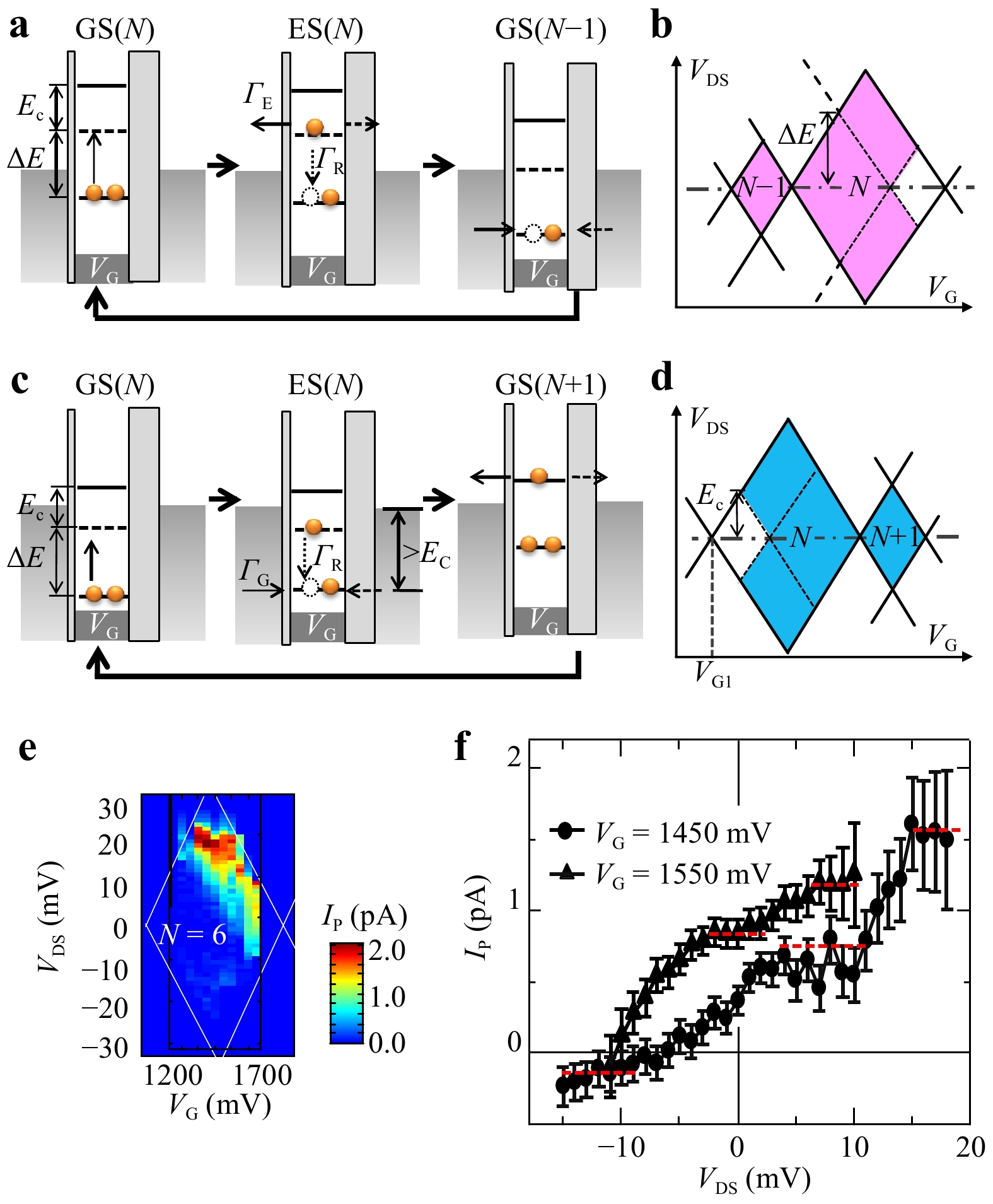
Fig. 5
a Energy band diagram of an InAs QD-SET for the “N → N − 1” process in THz photoexcitation49. b Photocurrent distribution with respect to the bias voltage (VDS) and gate voltage (VG) for the “N → N − 1” process49. c Energy band diagram of an InAs QD-SET for the “N → N + 1” process49. d Photocurrent distribution for the “N → N + 1” process49. e Measured THz-induced photocurrent distribution49. f THz-induced photocurrent measured with respect to VDS51. Images reprinted with the following permissions: a−e from ACS and f from AIP.Photocurrent spectra can be obtained using a Fourier transform spectrometer49, as shown in Fig. 6a. When the electron number in the QD (N) is six, the s- and p-shells in the QD are fully occupied. Three photocurrent peaks are present at slightly different photon energies. When VG is swept to modulate the electrostatic potential in the QD, the relative heights of the three peaks vary, but their photon energies remain constant. The three photocurrent peaks can be explained by the three transitions allowed by the optical selection rule for intersublevel photoexcitation. As shown in Fig. 6b, the THz field of this experimental setup is polarized along the source/drain nanogap electrodes, and only three dipole transitions are allowed when N = 6, as shown in Fig. 6c. Fig. 6c demonstrates that THz-SETS is a powerful tool for resolving very small energy splitting caused by the asymmetry in the shape of the QD.
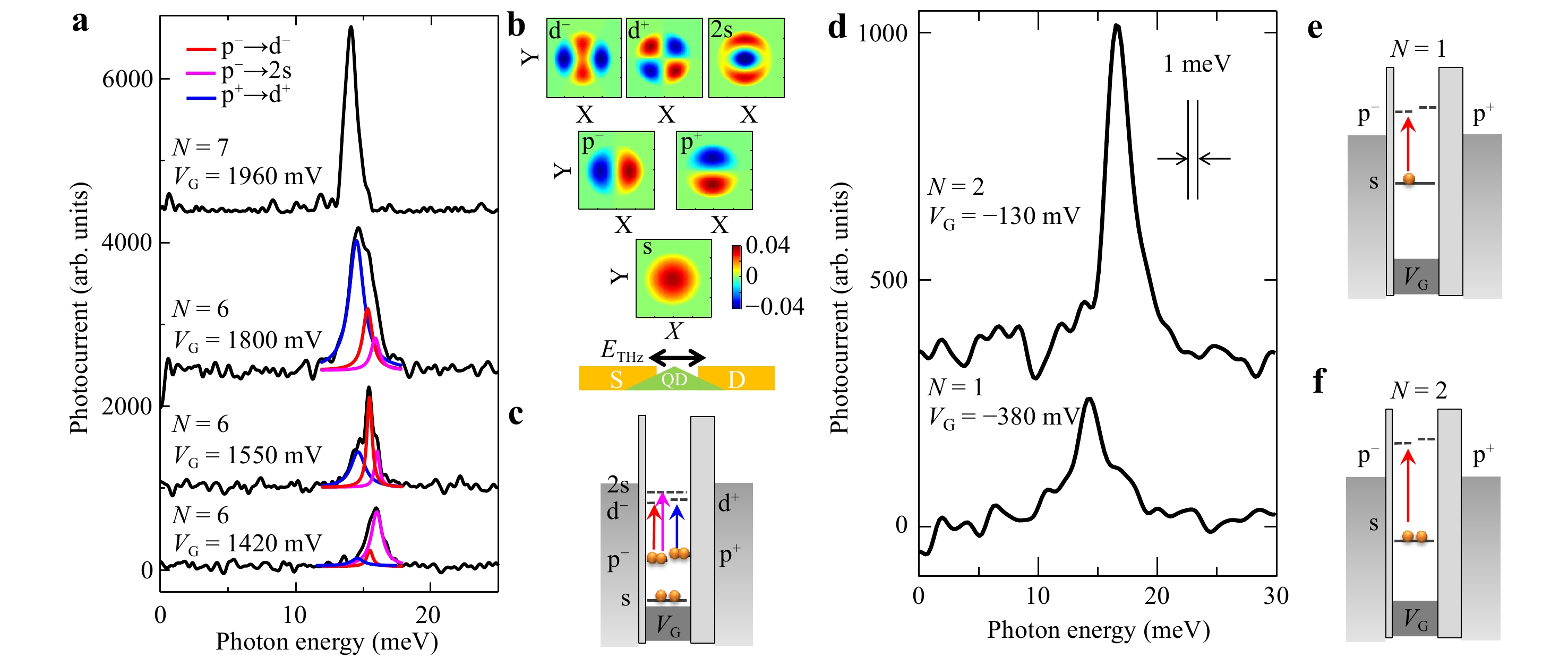
Fig. 6
a Photocurrent spectra of a QD when N = 6. The black, red, and blue curves show the three photocurrent peaks isolated from the spectra corresponding to the transitions between different subshells in the QD49. b Schematic illustrating the structure of a QD-SET. The THz field is always polarized along the direction of the source/drain electrodes49. c Energy band diagram of the QD-SET when N = 6. The black, blue, and red arrows indicate the three allowed transitions49. d Photocurrent spectra measured in an InAs QD-SET at various electron numbers (N = 1, 2)52. e, f Energy band diagrams of a QD-SET showing the intersublevel transitions for N = 1 and N = 2, respectively58. Images reprinted with the following permissions: a−c from ACS and d−f from APS.Another advantage of THz-SETS is that the electron number in the QD can be precisely controlled by VG. This is crucial for studying QDs or other zero-dimensional nanomaterials because both the optical and electrical properties are strongly affected by electron–electron interactions. A simple example of electron–electron interactions in QDs is shown in Fig. 6d−f. Fig. 6d plots the photocurrent spectra measured in a QD-SET when setting N = 1 and N = 2 by modulating VG50. As shown, photocurrent peaks are observed at different photon energies, ~14.3 meV for N = 1 and ~16.7 meV for N = 2. As schematically shown in Fig. 6e, f, the QD can accommodate two electrons in the ground state (s-state). The optical selection rule allows only one transition from the s-state to the p-state because the THz field is polarized along the source/drain nanogap electrodes. Therefore, the two photocurrent spectra shown in Fig. 6d arise from the same transition but with different electron numbers. The different photon energies imply that adding or removing a single electron to/from the QD substantially changes the THz photoexcitation energy through electron–electron interactions. This effect is important for the design of THz sensors or emitters using intersublevel transitions in zero-dimensional nanomaterials.
-
Spectroscopy at the single-molecule level provides key knowledge for customized medical, genomic, chemical, and quantum information technologies. However, there is a very large mismatch between the wavelength of a THz electromagnetic wave (~100 μm) and the size of a single molecule (~1 nm), which makes efficient focusing of THz electromagnetic waves onto a single molecule extremely difficult owing to the diffraction limit. THz spectroscopy of single fullerene and single endohedral metallofullerene molecules was performed. Ultrafast motions were observed not only for the fullerene cage53 but also for the encapsulated metal atom54.
First, we discuss how THz excitation modifies electron transport through a single molecule51. Assume there are N electrons in the molecule and that the system is in the Coulomb blockade region, as shown in Fig. 7a. The LUMO is above the source/drain Fermi levels. Therefore, in the dark, a tunneling electron cannot enter the molecular state. However, when the molecule is illuminated by THz radiation, an electron can move into the LUMO by absorbing a quantum of molecular vibration (“vibron”). The electron excited to the LUMO level subsequently leaves the molecule and tunnels into one of the electrodes, as shown in Fig. 7b (vibron-assisted tunneling-in process). Similarly, when there are N + 1 electrons in the molecule, and VDS and VG are set in the Coulomb blockade region, the HOMO is below the Fermi levels (see Fig. 7c), and the electron in the HOMO cannot escape the molecule in the dark. However, when the molecule is illuminated by THz radiation, the electron in the molecule absorbs a vibron and can leave the molecule (vibron-assisted tunneling-out process). Subsequently, as shown in Fig. 7d, the empty HOMO is refilled by a new tunneling electron from one of the electrodes. Fig. 7e, f show maps for the dark current and the THz-induced photocurrent measured as a function of VG and VDS on a single-molecule transistor (SMT)54. In Fig. 7e, the boundaries of the Coulomb diamonds are clearly shown, and it is evident that the polarity of the dark current follows the polarity of VDS. In contrast, as shown in Fig. 7f, the THz-induced photocurrent does not depend on the bias voltage for the range plotted in the figure, indicating that a portion of the photocurrent arises from the photovoltaic mechanism, similar to the photocurrent observed in QD-SETs51.
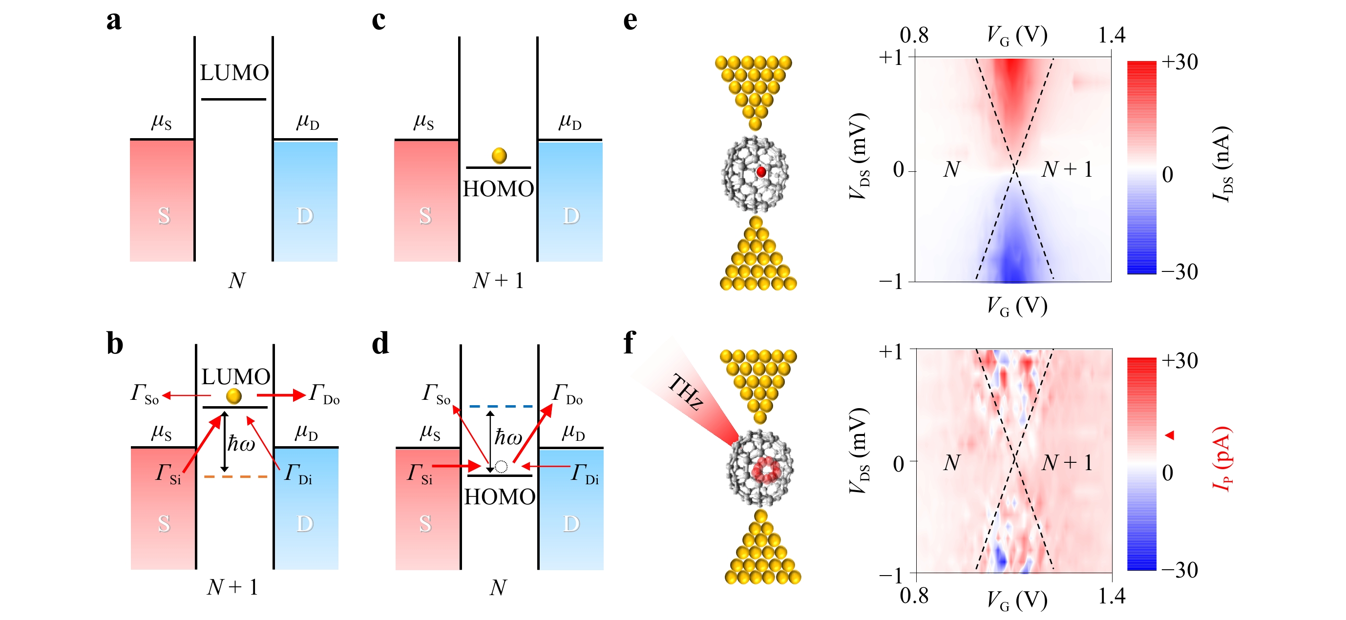
Fig. 7
a, b THz-induced vibron-assisted tunneling process when VG is on the left side of the charge degeneracy point. c, d THz-induced vibron-assisted tunneling process when VG is on the right side of the charge degeneracy point. ΓSi: tunnel-in rate from the source; ΓDi: tunnel-in rate from the drain; ΓSo: tunnel-out rate to the source; ΓDo: tunnel-out rate to the drain54. Maps of the e dark current (IDS) and f THz-induced photocurrent (IP) of an SMT as a function of VDS and VG. Images reprinted with the following permissions: a−f from IOP.Fig. 8a shows an autocorrelation trace of the THz-induced photocurrent signal measured on a C60 SMT. The trace shows quasi-oscillatory behavior with periods of ~1 and ~2 ps. The corresponding Fourier spectrum in Fig. 8b exhibits two low-energy peaks at ~2 and ~4 meV, which arise from the THz center-of-mass nanomechanical oscillation of the fullerene cage53. When a C60 molecule is captured on the surface of the Au nanogap electrodes, the C60 molecule experiences a quasi-parabolic van der Waals potential, which gives rise to a quasi-harmonic oscillation of the entire C60 molecule against the Au wall (center-of-mass oscillation). When the electron number in the molecule changes, the profile of the van der Waals potential may be modified. As shown in Fig. 8b, the photocurrent peaks at ~2 and ~4 meV are both finely split into two peaks. The observed peak splitting agrees well with the calculated change in the curvature of the quasi-harmonic van der Waals potential. This observation demonstrates that even the difference in the vibrational frequency caused by single-electron charging in the molecule can be detected by THz-SETS using nanogap electrodes53.
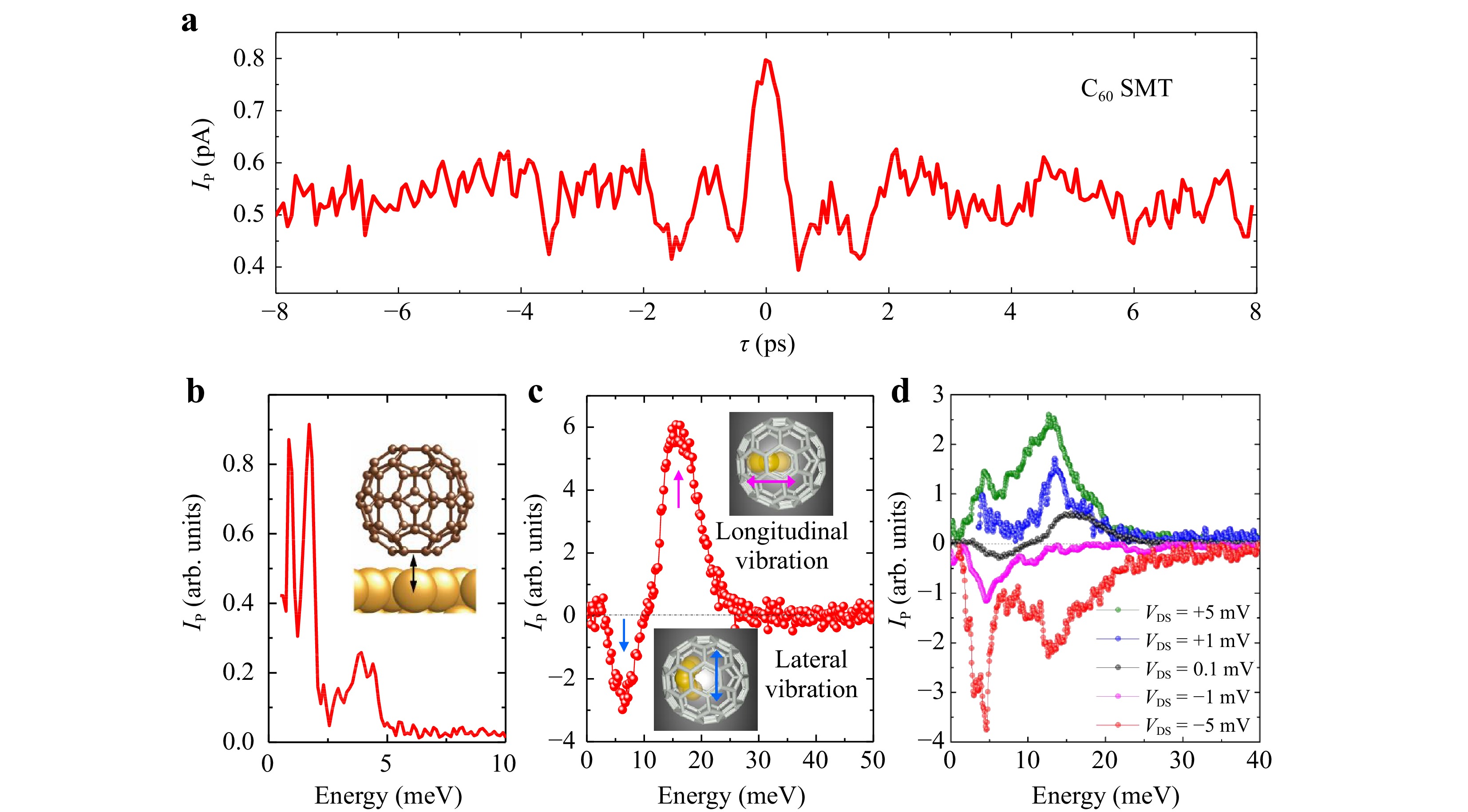
Fig. 8
a Quasi-autocorrelation trace (interferogram) of the THz-induced photocurrent measured on a C60 SMT. τ is the time difference between the two consecutive applied THz pulses. b Fourier spectrum of the interferogram shown in a. The spectrum exhibits sharp peaks at ~2 and ~4 meV with very fine peak splitting53. c THz-induced photocurrent spectrum of an SMT that consists of a single Ce@C82 molecule54. d Magnitudes of the two photocurrent peaks as a function of VDS (−5 mV < VDS < 5 mV)65. Images reprinted with the following permissions: a and b from Springer Nature and c and d from IOP.Furthermore, THz-SETS can reveal the dynamics of a single atom. A single Ce@C82 fullerene molecule was captured by a sub-nm gap between metal electrodes and excited by a THz electromagnetic wave to probe the motion of the Ce atom54. Two photocurrent peaks in the THz frequency range were observed, as shown in Fig. 8c, d. The first peak at ~5 meV is assigned to the vibration of the trapped Ce atom in the lateral direction, and the second broader peak at ~15 meV is attributed to the vibration of the Ce atom in the longitudinal direction54, 64, 65. As seen in Fig. 8c, d, the two peaks are broader than the photocurrent peaks in Fig. 8b. The broad peaks suggest that the vibrational modes of the Ce atom have very short coherence times, which is probably due to the chaotic interactions between the elastic fullerene cage and the Ce atom. These results demonstrate that THz-SETS has an extremely high sensitivity and can sense the dynamic motion of a single atom.
These examples clearly demonstrate that although THz-SETS is not capable of imaging, it can provide invaluable information on the electronic and vibronic dynamics in deep-nm-systems with a sub-picosecond time resolution.
-
In summary, we have reviewed a novel THz spectroscopy technique for deep-nm-scale systems by combining antenna-integrated metal nanogap electrodes with an SET structure. Metal nanogap electrodes can capture a single nm-scale system, such as a semiconductor QD or a single molecule. The THz field is tightly confined in the metal nanogap region and is enhanced by a factor of ~λ/d (λ: THz wavelength, d: gap size), which can reach ~105. Even tiny absorption of THz radiation by a single nm-scale system can be detected by measuring the THz-induced photocurrent through the system. Taking advantage of the ultrasmall dark current in the Coulomb blockade regions in single-electron tunneling, THz dynamics, such as intersublevel transitions in single QDs and vibrational excitations in single molecules, can be studied. The THz-SETS scheme can achieve THz spectroscopy with simultaneous sub-nm-scale spatial resolution and sub-picosecond time resolution.
The ability to measure the properties of single molecules may be useful for studying complex molecules, such as DNA and biological macromolecules, at the single-molecule level. In conventional THz spectroscopy, THz plasmonic nanoantennas66, 67 and THz metamaterials68−71 have been used to enhance THz fields for the detection of microorganisms, organic molecules, and biomolecules. However, ensemble measurements contain information on both intra- and intermolecular vibrations. Because of the complex nature of biomolecules, these two types of vibrations are easily coupled and exhibit very broad absorption peaks, which makes THz data interpretation difficult. Measuring such complex molecules at the single-molecule level is promising because it can remove the effects of both intermolecular excitations and inhomogeneous broadening.
There are several issues that must be solved for nm-scale THz spectroscopy. One issue is how to image and capture targeted ultrasmall nanostructures (such as single molecules) while maintaining the ability to modulate the electrostatic potential and the electron number in the nanostructures. As mentioned previously, s-SNOM and STM are excellent at imaging nanostructures46. However, a major drawback is that it is difficult to modulate the electronic states of the sample using these nanoprobe techniques because they lack gate electrodes. A few novel methods based on nanoprobe techniques have been developed72−75 that include both “imaging” and “gating” functions simultaneously. However, realizing this dual functionality at the single-molecule level remains a major challenge. The SET geometry can easily modulate the electronic states in single molecules. However, capturing single molecules using nanogap electrodes is a stochastic process, and contact cannot be made at a targeted molecule. Therefore, combining the two types of measurements to realize a more versatile nanoscale THz spectroscopy system in the near future is highly desirable.
We conceive a new direction for THz-SETS: the control of the electronic/vibronic states in nm-scale systems, which will be critical for future quantum information technologies. When THz photons strongly couple with electrons in nanostructures76, 77, they can form a quantum hybrid system: THz cavity quantum electrodynamics (cavity-QED)78−80. The strong electron–photon coupling in THz cavity-QED enables the operation of the cavity quantum dynamic ground state78 and is expected to be useful for transferring quantum information from electrons to photons and vice versa81. This is a new technology for quantum information processing. THz-SETS is attractive for THz cavity-QED because it can tightly focus THz radiation onto a single quantum nanostructure. Furthermore, its gating ability enables the manipulation of quantum states using simple electrical gating. However, the quality (Q)-factors of standard bowtie-type THz antennas used for THz-SETS are too small to achieve strong electron–photon coupling (typically Q-factor of ~1). By combining the present THz-SETS with high Q-factor THz cavities, such as THz metamaterials78, 79 and THz photonic crystals80, a powerful platform can be developed for studying THz cavity-QED.
Nanoscale THz spectroscopy also shows promise for the investigation of THz nonlinear effects, in which an intense THz field is utilized to reveal new light–matter interactions82, 83. Many exciting findings have been reported, such as the use of intense THz pulses to coherently control the switching of the polarization in ferroelectric materials84, 85 and to excite/control spin waves in antiferromagnetic materials86−91. Such findings indicate that intense THz waves can control material properties and even lattice structures. The nanoscale THz spectroscopy introduced here can extend such nonlinear control to nm-scale regions. In particular, when the THz field is strongly squeezed into sub-nm regions, it is greatly enhanced by a factor of ~105. The combination of a recently developed technique to generate very intense THz pulses83, 92, 93 with such a large field enhancement effect in nanogaps offers a unique opportunity to study novel material properties in the extremely high THz electric field regime (1−100 GV/cm).
In conclusion, THz-SETS provides a powerful method for squeezing THz electromagnetic waves into nm-scale regions and detecting ultrasmall THz absorption with high sensitivity. It is promising for the investigation of the nm- and sub-nm-scale THz dynamics of not only single quantum nanostructures but also single molecules, which will extend the great success of traditional THz spectroscopy to the deep-nm-scale regime. Such nm-scale THz spectroscopy provides a key scientific foundation for nanoscience and nanotechnology.
-
The authors thank Y. Arakawa, G. Bastard, H. Q. Xu, Y. Hirayama, K. Yoshida, K. Shibata, and T. Tsusugaya for their fruitful discussions. This work was supported by MEXT KAKENHI Grant Number JP15H05868, JSPS KAKENHI Grant Numbers JP20H05660, JP17H01038, JP16H06709, and the Canon Science Foundation.
Deep-nanometer-scale terahertz spectroscopy using a transistor geometry with metal nanogap electrodes
-
Ya Zhang1, *, ,
 ,
, - Shaoqing Du2, *, ,
-
Kazuhiko Hirakawa2, 3, *, ,
- Light: Advanced Manufacturing 2, Article number: (2021)
- Received: 10 January 2021
- Revised: 15 November 2021
- Accepted: 28 November 2021 Published online: 13 December 2021
doi: https://doi.org/10.37188/lam.2021.031
Abstract: Terahertz (THz) spectroscopy is a powerful tool for characterizing electronic properties and vibronic excitations in various types of solids, liquids, and gases, and it has been extensively used not only for basic science but also for industrial applications. Recently, it has become necessary to understand electronic and vibronic excitations at the nanometer (nm) scale to realize state-of-the-art quantum nanodevices and the synthesis of new molecules for medicine. However, it is challenging to perform THz spectroscopy at the nm scale because the diffraction limit of electromagnetic waves hinders tight focusing of THz radiation at the nm scale. Here, we introduce a novel technique for THz spectroscopy using metal nanogap electrodes. Metal nanogap electrodes integrated with a THz antenna are employed to capture sensing targets, such as a single semiconductor quantum dot (QD) or molecule. Even extremely weak THz absorption can be detected with high sensitivity by measuring the THz-induced photocurrent through the sensing target. Taking advantage of THz-induced photocurrent spectroscopy, the electronic structures in single QDs as well as the vibrational states in single molecules are systematically investigated. The present characterization technology for nm-scale systems provides a key scientific foundation for creating nanodevices with new functions.
Research Summary
Deep-nanoscale THz spectroscopy: going much beyond the diffraction limit
THz spectroscopy has become a powerful tool for characterizing electronic properties and vibronic excitations in various kinds of materials. Recently, the need to understand electronic and vibronic excitations at the nanometer (nm) scale has emerged for realization of state-of-the-art quantum nanodevices and synthesis of new molecules for medicine. However, performing THz spectroscopy at the nm scale is extremely challenging because the diffraction limit of electromagnetic waves hinders tight focusing of THz radiation down to the nm scale. A team from University of Tokyo and Tokyo University of Agriculture and Technology has introduced a novel technique of using metal nanogap electrodes for deep-nanoscale THz spectroscopy, which provides a major scientific basis for creating nanodevices with new functions.


Rights and permissions
Open Access This article is licensed under a Creative Commons Attribution 4.0 International License, which permits use, sharing, adaptation, distribution and reproduction in any medium or format, as long as you give appropriate credit to the original author(s) and the source, provide a link to the Creative Commons license, and indicate if changes were made. The images or other third party material in this article are included in the article′s Creative Commons license, unless indicated otherwise in a credit line to the material. If material is not included in the article′s Creative Commons license and your intended use is not permitted by statutory regulation or exceeds the permitted use, you will need to obtain permission directly from the copyright holder. To view a copy of this license, visit http://creativecommons.org/licenses/by/4.0/.

 DownLoad: