


-
Artificial intelligence (AI) proliferation has catalysed a significant increase in data generation, consequently amplifying the demand for robust data centre traffic capabilities1. As the industry anticipates further data traffic escalation, the commercial adoption of 400 Gbit/s per lane intensity-modulated direct detection (IM/DD) high-speed optics is expected by 20272. To enable this 400 Gbit/s per lane IM/DD transmission, employing high-bandwidth electro-optic modulators with a bandwidth above 100 GHz is essential3−5.
Thin-film lithium niobate (TFLN) is a promising platform for high bandwidth electro-optic modulators because of its wide transparency window, strong electro-optical coefficient (γ33 = 30.8 pm/V at λ = 630 nm), and high refractive index contrast (Δn ≈ 0.7 at λ = 1550 nm)6,7. Based on TFLN, several modulators with bandwidths h of 100 GHz8, > 100 GHz9, and 170 GHz10 have been reported in previous studies. However, these high-performance modulators were fabricated using an electron-beam lithography system, which is unsuitable for high-volume manufacturing owing to its limited throughput. Lithography is widely used in the volume manufacturing of integrated circuits (ICs). It has also been applied to fabricate TFLN photonic integrated circuits11,12. However, not all prior studies achieved volume manufacturing of TFLN modulators with a bandwidth > 110 GHz. This study demonstrates a high-yield, low-loss, and high-bandwidth photonic platform based on 4-inch TFLN wafers with a quartz handle layer.
TFLN modulators with bandwidth greater than 110 GHz and half-wave voltage (Vπ) less than 3 V are achieved on this platform. Additionally, by utilising deep-ultraviolet (DUV) lithography and metal lift-off processes, the platform can be extended to larger wafer sizes, such as 6 or 8 in. Such wafer-level throughput of a 110 GHz electro-optic modulator can substantially increase the capabilities of data centre optical interconnects.
-
Fig. 1 shows the schematic of the proposed modulator with capacitance-loaded traveling-wave electrodes (CL- TWEs). CL-TWEs comprise a coplanar transmission waveguide (CPW) and a series of segmented electrodes arranged periodically with a period of r. The optical group index of the proposed waveguide is 2.23-2.25. Using CL-TWEs, the microwave index of the travelling wave electrode on TFLN wafers with a quartz handle can be tuned in the 2.2-2.3 range, precisely matching the optical group velocity of the TFLN waveguides. Meanwhile, the segmented electrodes prevent the electrical current from flowing into the narrow-gap region, decreasing the ohmic loss of the travelling-wave electrodes.
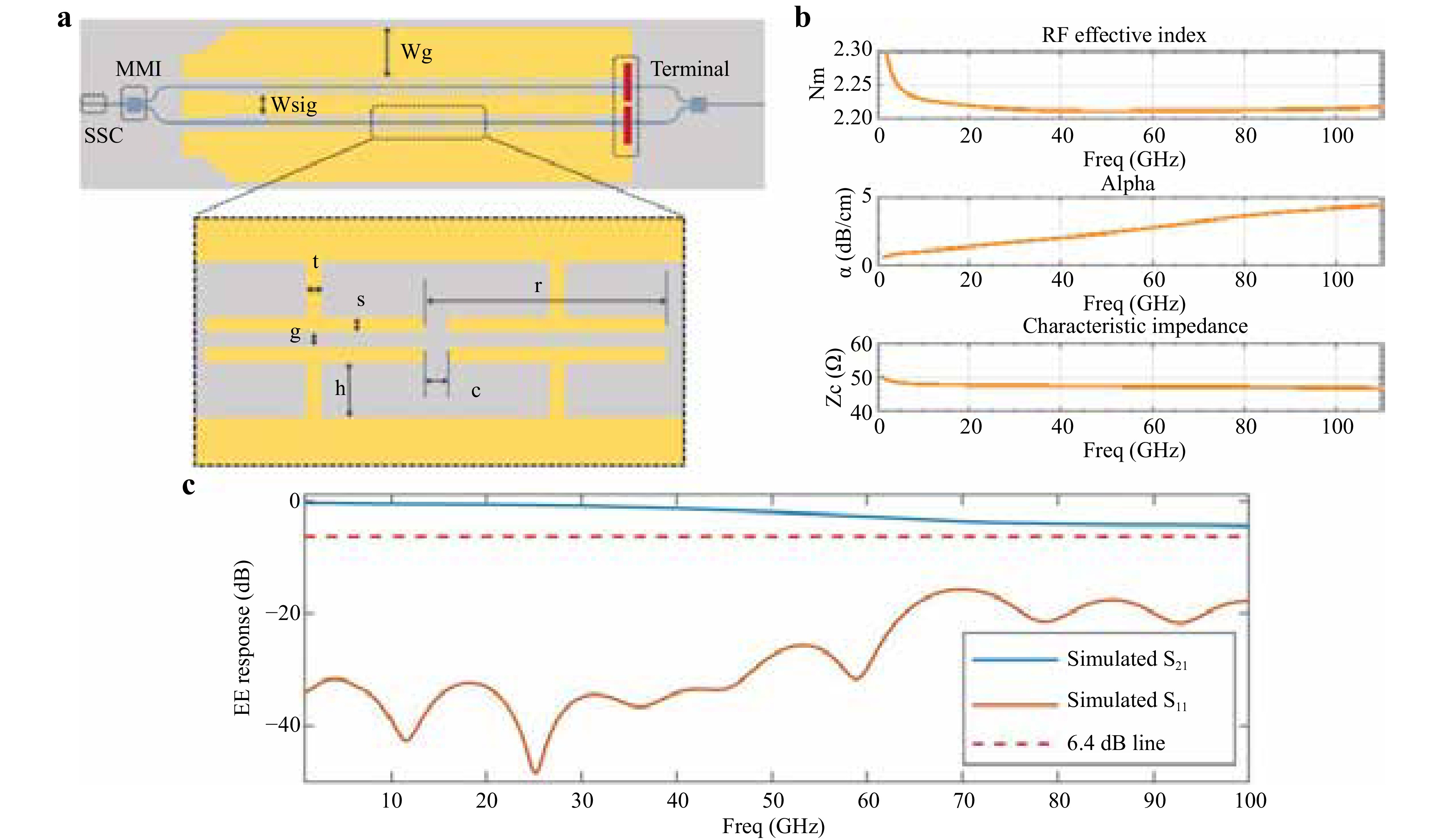
Fig. 1 Layout schematic of the TFLN modulator and parameters extracted by simulation. a The schematic of the ‘T-shaped’ modulator, where Wg = 200 μm, Wsig = 80 μm, t = 2.3 μm, h = 10 μm, s = 2.3 μm, g = 3 μm, r = 50 μm, c = 5 μm. b Parameters extracted from simulation, featuring the effective index of microwave is 2.22, alpha is4.4 dB/cm at 110 GHz and characteristic impedance is 47 Ω. c The simulation results for S21 and S11 of the electrode.
Hence, the CL-TWEs on the TFLN wafers with quartz handle enable a broad bandwidth > 110 GHz9,13.
CL-TWEs with a length of 600 μm were simulated using commercial finite element methods. For CL-TWE on TFLN wafers with quartz handle, the film stacks were Au: 1 μm, SiO2: 1 μm, LN: 360 nm, SiO2: 2.5 μm and quartz: 500 μm. The width of the CPW signal line is 80 μm, and the width of the ground electrode is 200 μm. Fig. 1a shows the magnified view of the segmented electrodes, where t = 2.3 μm, h = 10 μm, s = 2.3 μm, g = 3 μm, r = 50 μm and c = 5 μm. As illustrated in Fig. 1b, the simulation results indicate that the effective microwave index is 2.22, the microwave loss is 4.4 dB/cm at 110 GHz, and the characteristic impedance is 47 Ω. Fig. 1c shows the simulation results for the S21 and S11 electrodes. S211 of the electrode drops 4.5 dB at 100 GHz, supporting an electro-optical bandwidth greater than 100 GHz. In other words, CL-TWEs with the proposed parameters can simultaneously achieve low microwave loss, impedance, and velocity matching, enabling a large bandwidth.
A commercial 4-inch x-cut TFLN wafer with a 360-nm thin film of LN and a 2.5 µm buried oxide (BOX) layer is used as the substrate. The wafer handle is made of quartz, exhibiting a low microwave absorption tangent of 10−5. In comparison, the microwave absorption tangent of Si is 0.043. By using a quartz substrate, microwave loss can be effectively suppressed at high frequencies. This is crucial for obtaining a modulator with a bandwidth exceeding 110 GHz. First, the LN waveguides were defined by DUV stepper lithography based on a 193 nm ArF excimer laser and Ar+ based reactive ion etching. Using DUV, in contrast to commonly employed electron beam lithography, enables a dramatic increase in fabrication throughput, stability, and reproducibility, which is essential for large-volume manufacturing. Fig. 2d shows the scanning electron micrographs (SEM) of the LN waveguide with smooth sidewalls. After the first lithography and etching, the LN waveguides with a top width of 2.5 µm, slab thickness of 180 nm, and rib height of 180 nm are obtained. The slab with a thickness of 180 nm was then patterned and etched to form the edge couplers. After patterning the LN waveguides and edge couplers, a PECVD SiO2 film of 3 µm thickness is deposited as the cladding layer. Such a thick cladding layer is utilised to maintain a large optical mode, which leads to high coupling efficiency. However, the thick cladding layer separates the electrodes and waveguides, decreasing the modulation efficiency. Hence, we etch the SiO2 with a depth of 2 µm to open windows for metal deposition. Subsequently, a 180-nm-thick NiCr layer was deposited as the terminal resistor and thermal electrode. Finally, a lift-off process produces the 1-μm-thick gold transmission lines.
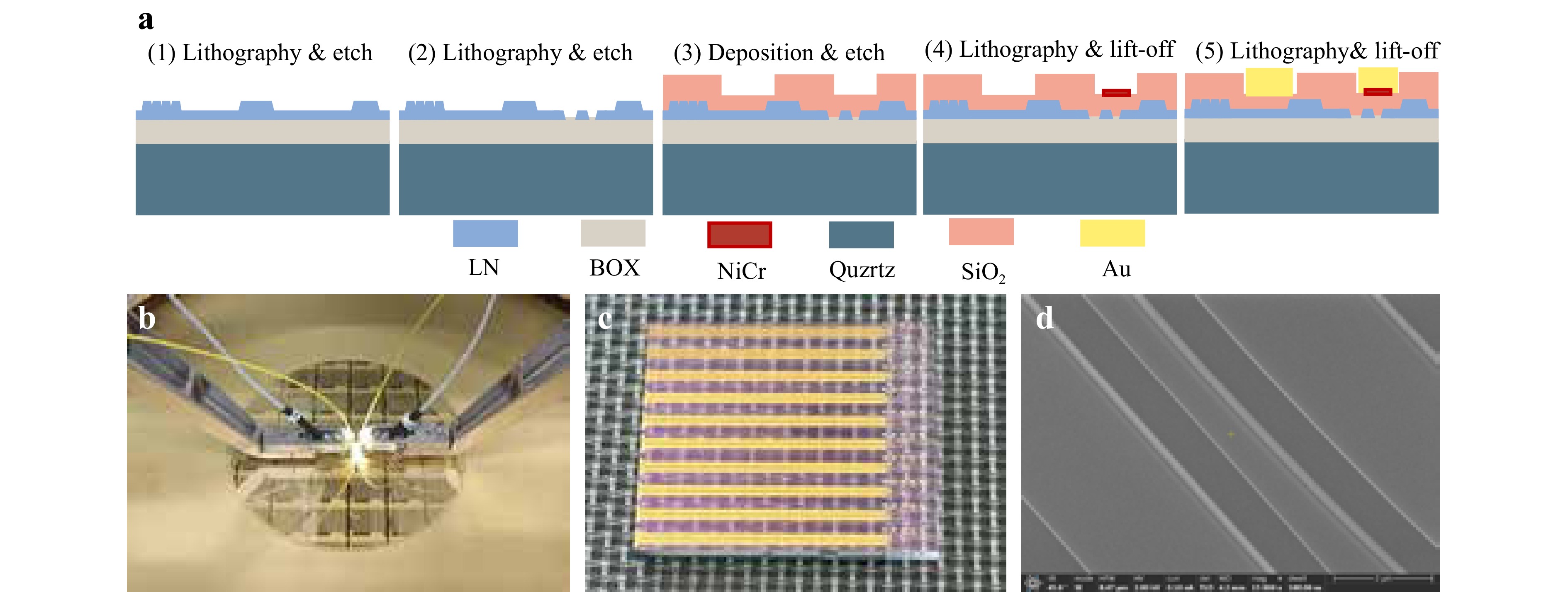
Fig. 2 Wafer-scale TFLN process flow and photos of a wafer. a Process flow of TFLN wafer. b Wafer under wafer-scale test. c Single block photograph. d SEM of LN waveguide.
-
Using the wafer-scale TFLN process, we can integrate components, including splitters, filters, thermal shifters, edge couplers, grating couplers, and high-bandwidth modulators, on the TFLN wafer and achieve on-chip systems for emergency applications. The fabricated TFLN wafer underwent characterisation to ascertain the optical loss of 1-μm-wide waveguides across the 4-inch wafers. Fig. 2b shows the fabricated TFLN wafer subjected to wafer-scale testing. A mapping of the fabricated wafer is shown in Fig. 3a. The wafer was composed of 12 chips on the DUV stepper reticle, each measuring 22 × 22 mm2 and incorporating modulators, couplers, and spiral waveguides. Fig. 3b offers a microscope image of the spiral TFLN waveguides, which are densely packed with a waveguide width of 1 μm and a gap distance of 13 μm. The DUV stepper uniformly inscribes the reticle pattern across the 4-inch wafer in discrete fields.
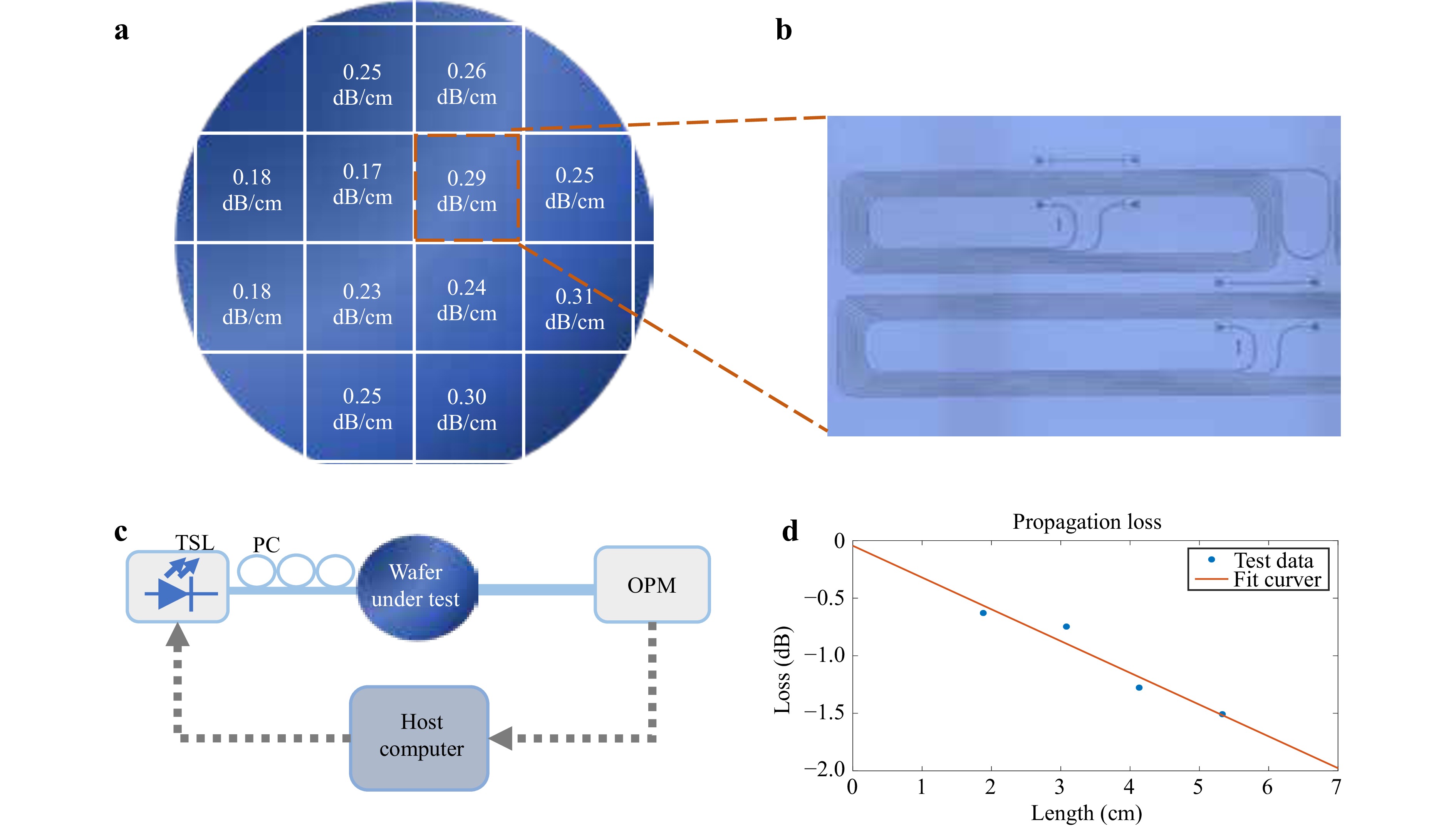
Fig. 3 Wafer-scale characterization of the optical propagation. a DUV stepper exposure Layout and 1 µm waveguide propagation loss test results of each block. b Micrograph of spiral waveguide. c Propagation loss measurement, tunable laser (TL), polarization controller (PC), optical power meter (OPM). d The test data and linear fitting curve of one block.
The cut-back method was used to estimate the propagation loss. The experimental setup is shown in Fig. 3c. This was performed by measuring the transmission through spiral waveguides with lengths of 2.83 cm, 3.75 cm, 5.59 cm, and 7.43 cm. The four spiral waveguides had the same bending waveguide region but different straight waveguide lengths. Therefore, the bending loss was calibrated. Two grating couplers were connected to a single-mode waveguide to achieve fibre–chip–fibre coupling. Fig. 3d shows one of the cut-back loss measurements for the 180 nm × 1000 nm rib TFLN waveguides at a wavelength of 1550 nm, calibrated using the adjacent reference waveguide. The propagation loss was determined to be 0.2 dB/cm, and waveguide losses of other chips are shown in Fig. 3a by using the same measurement method. As the figure shows, a low-loss waveguide yields a propagation loss of < 0.4 dB/cm.
Following the testing procedure, the wafer was carefully diced to yield individual chips, as shown in Fig. 2c. Each chip contained ten electro-optic (EO) modulators, as shown in Fig. 4a. Subsequently, the EO response of the modulator was measured. The input light from a tunable laser (TL), set to a wavelength of 1550 nm, was directed through a polarisation controller (PC) to align its polarisation. Subsequently, light is efficiently coupled to the chip using an edge coupler. A small RF signal from the vector network analyser (VNA) was sent to the chip through a 110 GHz probe. The modulated light is then propagated through the other edge coupler. A Keysight 110 GHz lightwave component analyser (LCA, N4372E) was used to receive the output signal. As shown in Fig. 4b, the EO response shows only a 2.3 dB roll-off at 110 GHz. This indicates that the 3 dB EO modulation bandwidth of the proposed modulator is larger than 110 GHz, which enables 400 Gbit/s/lane IMDD transmission. Meanwhile, the half-wave voltages Vπ were also measured for the proposed modulator using a 500 kHz triangular voltage sweep. As shown in Fig. 4c, the Vπ value for the modulators is 2.92 V, corresponding to a VπLof 2.92V cm. Moreover, the EO bandwidth and Vπ of the modulators among the wafer were measured. Fig. 5a, b shows the wafer-scale map of modulators EO bandwidth and Vπ. We define the yield of the modulator as the ratio between the number of modulators with bandwidth > 110 GHz and Vπ < 3V to the total number of measured chips. In the present study, the yield was calculated to be 6/12 = 50%.
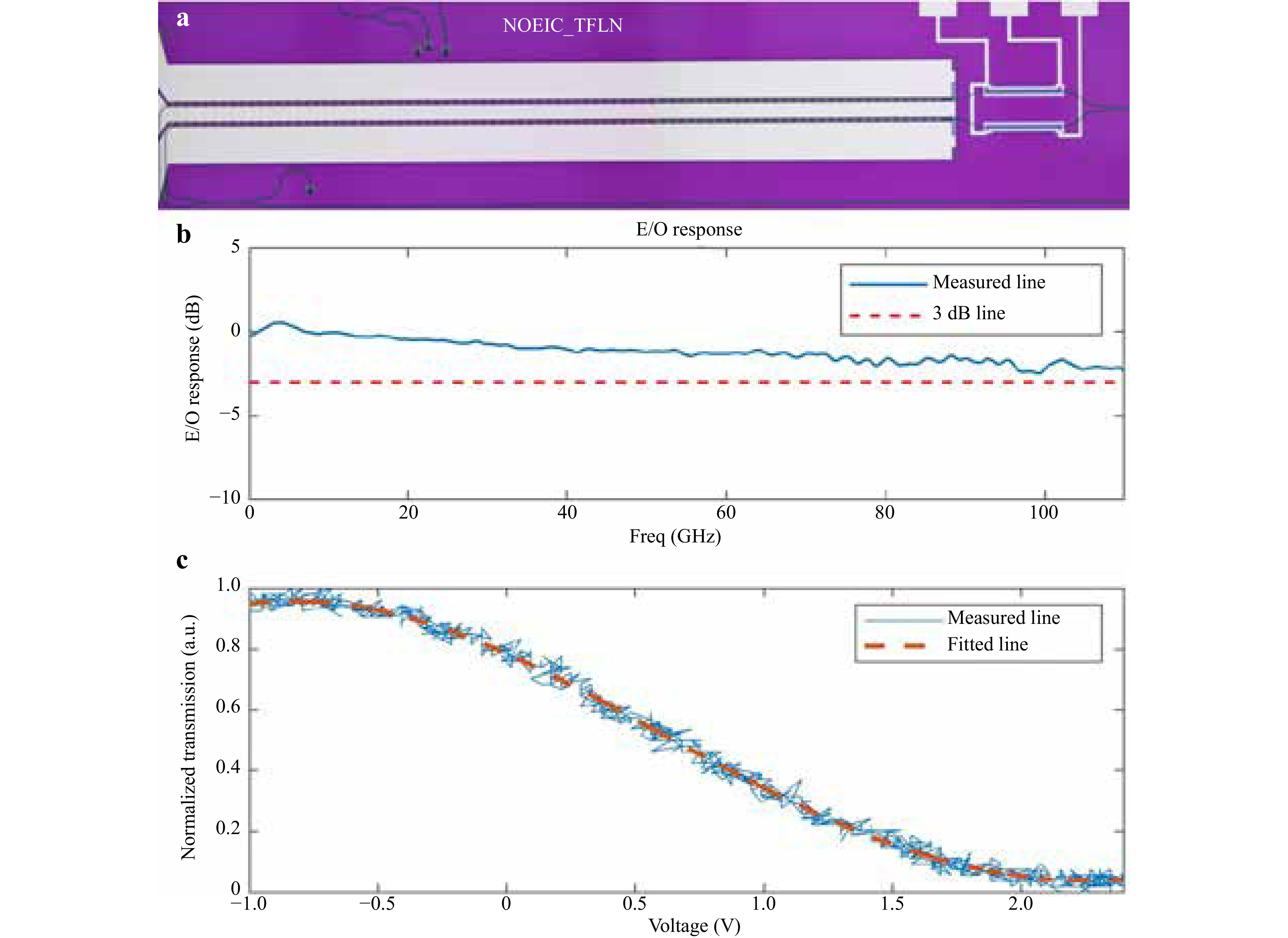
Fig. 4 TFLN modulator. a Micrograph of a Mach- Zehnder modulator. b 3 dB EO response beyond 110 GHz. c Half-wave voltage at 1 GHz, 2.92 V.
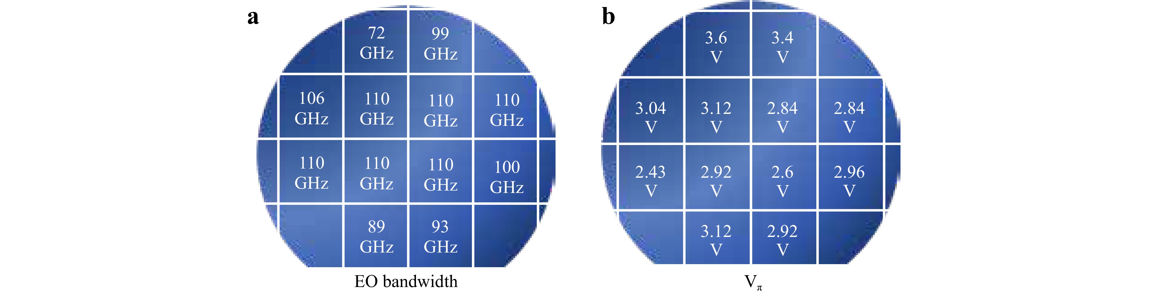
Fig. 5 a Wafer-scale map of modulators EO bandwidth. b Wafer-scale map of Vπ.
Moreover, the high-bandwidth electro-optic modulator was packaged as a device, as shown in Fig. 6a. Edge couplers were fabricated for efficient coupling with ultrahigh numerical aperture (UHNA) fibres (measuring 2 dB/facet). The total fibre-to-fibre loss was measured to be 6.5 dB. A 1-mm RF connector was used to apply the RF signals. The EO response of the modulator device was measured using a 110 GHz LCA. Fig. 6b shows the EO response has a 3.6 dB roll-off at 110 GHz. The 3 dB EO bandwidth of the modulator device was 95 GHz. Moreover, the bandwidth of the modulator device can be improved by improving the wire-bonding quality between the modulator chip and transmission line on the packaging substrate.
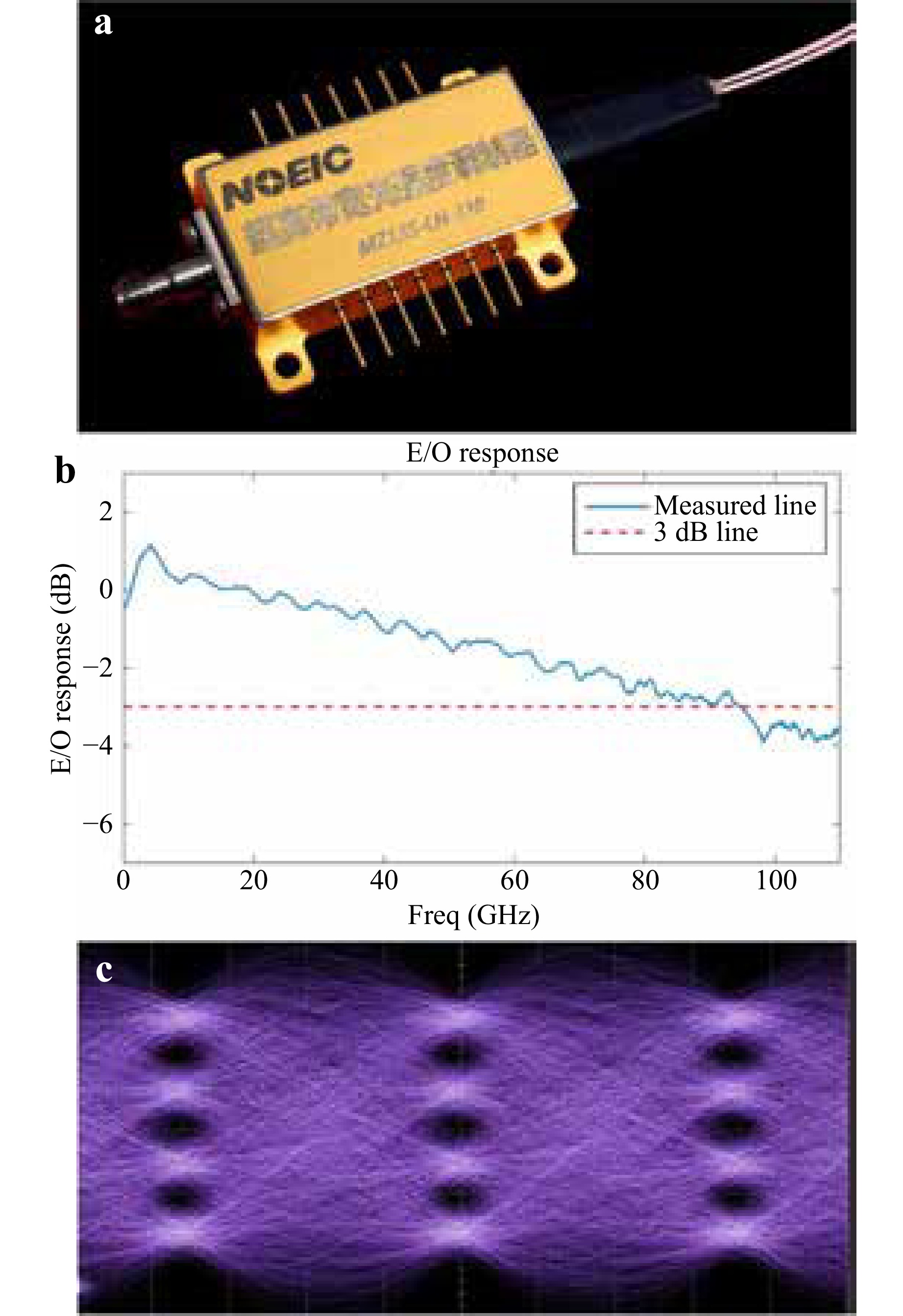
Fig. 6 The packaged high-bandwidth EO modulator. a High-Bandwidth EO modulator package photograph. b EO response S21 of the modulator. c190 Gbaud PAM-4 eye diagrams demonstrating modulator performance.
The modulator device was evaluated to verify the high-speed data transmission of the fabricated modulators. A data signal was generated during the measurements using a 224 GS/s arbitrary wave generator (AWG, Keysight M8199B) with an analogue bandwidth of 80 GHz. After amplification, the RF signal was applied to the device through a 1-mm RF connector. A TL of approximately 10 dBm was used as the light input, and the modulated light was detected using a series wide-bandwidth oscilloscope (Keysight, N1032A) with a 90 GHz sampling module. Off-line DSP is utilised jointly on both the Tx and Rx sides to optimise the performance of the transmission system. In the Tx DSP, a pseudo-random bit sequence (PRBS) PAM-4 signal is generated with a word length 215. A root-raised cosine (RRC) filter and pre-emphasis were employed to eliminate the bandwidth limitation of the MZM and end-to-end transmission system. On the Rx side, the received data are first resampled and synchronised. Then, a 21-tap adaptive feed-forward equaliser (FFE) is utilised to compensate for the linear impairment generated in high-speed transmission. The eye diagrams for the 190 Gbaud PAM- 4 signals after device operation are shown in Fig. 6c. A sinx/x function built into an oscilloscope (Keysight N1032A) was used for the measurement. The experimental results indicate that the optical extinction ratio (ER) is 3.212 dB, and the transmitter and dispersion eye closures quaternary ratio (TDECQ) is 3.14 dB.
It is worth noting that the AWG limits the baud rate to 190 Gbaud, and the demonstrated modulator can support a higher baud rate, such as 200 Gbaud. The modulator under investigation is anticipated to facilitate optical transmission at speeds exceeding 400 Gb/s/lane using PAM4 modulation.
The performance of the modulator in this study was compared with that of previously reported TFLN modulators, as shown in Table 1. In previous studies, certain groups successfully demonstrated modulators with bandwidths exceeding 110 GHz. However, they were fabricated using an electron-beam lithography system, which is not conducive to high-volume manufacturing owing to its restricted throughput. Meanwhile, other groups have introduced high-volume manufacturing of TFLN modulators based on a wafer silicon handle; however, the bandwidths achieved were only approximately 40 GHz and 67 GHz. In this study, we accomplished volume manufacturing of 110 GHz modulators. The proposed device stands out for its exceptional combination of low insertion loss and half-wave voltage, which is pivotal for high-speed optical communication systems. This comparison underscores the innovative strides made by our modulator to enhance the efficiency and performance of TFLN-based platforms, offering a promising solution for next-generation optical communication applications.
Devices IL (dB) Vπ (V) Length (mm) Bandwidth (GHz) Transmission Throughput MZM (Quartz)9 14 2.3 10 > 50 / Low MZM14 17 3.4 5 > 67 / Low MZM11 8.35 3.5 5 > 40 / High MZM3 24 1.7 18 60 172 Gbaud PAM8 Low MZM15 8.2 2.2 10 > 67 56 Gbaud PAM16 Low MZM (Quartz)13 6.8 1 23.5 > 110 130 Gbaud 400QAM Low MZM10 16 6.6 5 170 80 Gbaud PAM8 Low MZM16 5 1.85 4 > 67 / High This work 6.5 2.92 10 > 110 190 Gbaud PAM4 High Table 1. Performance comparison of TFLN modulators
-
In conclusion, this work successfully demonstrated a high-volume, reproducible, wafer-scale manufacturing process for TFLN modulators with bandwidth exceeding 110 GHz. The fabricated waveguides exhibited low propagation loss (< 0.4 dB/cm) across the wafer. The modulator chip showed a low roll-off of only 2.3 dB at 110 GHz relative to a measured Vπ of 2.92 V at 1 GHz for a 10 mm device. Moreover, the packaged modulator device with EO bandwidth of 95 GHz enables the 190 Gbaud PAM4 optical transmission. his high wafer-level throughput of 110 GHz electro-optic modulators has the potential to enhance the capacity of data centre optical interconnects significantly.
-
National Key Research and Development Program of China (2022YFA1205101).
Volume manufacturing of thin-film lithium niobate modulators with bandwidth > 110 GHz based on 4-inch wafer with a quartz handle
- Light: Advanced Manufacturing , Article number: (2025)
- Received: 21 October 2024
- Revised: 09 May 2025
- Accepted: 22 May 2025 Published online: 15 August 2025
doi: https://doi.org/10.37188/lam.2025.047
Abstract: The continuous growth in data centre traffic, especially from artificial intelligence and machine learning workloads, is driving increased single carrier line rates. High-bandwidth electro-optic modulators are essential for supporting 400 Gbit/s per lane transmission. While recent advancements have demonstrated bandwidths greater than 110 GHz at the die level, this throughput is insufficient for current and future applications like data centre optical interconnects. This paper presents a photonic platform based on 4-inch thin-film lithium niobate wafers with a quartz substrate, offering high yield, low loss and high bandwidth. This platform achieves waveguide propagation loss of < 0.4 dB/cm. The thin-film lithium niobate modulators fabricated on this platform can attain a bandwidth exceeding 110 GHz and possess a half-wave voltage (Vπ) lower than 3 V, with the modulator yield reaching 50%. Additionally, by employing deep-ultraviolet lithography and a metal lift-off process, the platform can be extended to larger wafer sizes (e.g., 6 or 8 inches). This significant increase in wafer-level throughput for 110 GHz electro-optic modulators can greatly enhance data centre optical interconnect capabilities.
Rights and permissions
Open Access This article is licensed under a Creative Commons Attribution 4.0 International License, which permits use, sharing, adaptation, distribution and reproduction in any medium or format, as long as you give appropriate credit to the original author(s) and the source, provide a link to the Creative Commons license, and indicate if changes were made. The images or other third party material in this article are included in the article′s Creative Commons license, unless indicated otherwise in a credit line to the material. If material is not included in the article′s Creative Commons license and your intended use is not permitted by statutory regulation or exceeds the permitted use, you will need to obtain permission directly from the copyright holder. To view a copy of this license, visit http://creativecommons.org/licenses/by/4.0/.

 DownLoad: