


-
Functional terahertz (THz) and millimeter-wave (mmW) structures crucially rely on precisely defined three-dimensional (3D) freeform geometries that combine highly conducting metal elements with low-loss dielectrics. Outstanding geometrical precision can be achieved by direct-write multi-photon laser lithography (MPL)1,2, offering highest resolution on the sub-micrometer scale along with precise alignment of the fabricated structures to existing circuitry on the underlying substrate. These advantages have been extensively exploited in the field of photonic integration3, where 3D-printed waveguides, so-called photonic wire bonds (PWB)4–8, or facet-attached microlenses (FaML)9,10 offer interesting perspectives for scalable fully automated assembly of hybrid multi-chip systems. Transferring these concepts to THz assemblies, however, has so far been hindered by the lack of microfabrication techniques that can complement 3D-printed polymeric base structures by precisely defined highly conductive metal elements3,11–13. Specifically, while two-photon-induced reduction of metal salts has been exploited to generate free-standing 3D metal structures14,15 or to decorate the surfaces of 3D-printed polymer structures with local silver16–18 or platinum13 lines, the resulting surface quality and the conductivity of the metal parts are still insufficient for low-loss mmW or THz devices. Similar chemical reaction mechanisms can be used for fabricating gold-containing nanocomposite structures with 3D freeform shapes19. However, the electrical conductivity that can be achieved through such techniques is limited by the metal loading, which is generally dictated by the solubility of the metal ions12 in the respective photoresist. Moreover, when the incident laser beam interacts with already fabricated metal structures during printing, thermal effects and localized surface plasmon resonances can lead to aggregation and crystallization of metal nanoparticles, rendering these processes hard to control. Additionally, all aforementioned techniques have so far been limited to a rather small selection of metals such as silver14,16–18,20–24, gold15,19,25–28, palladium23,29,30, and platinum13,24,29, but are not available for more widely used materials in mmW and THz electronics such as copper or aluminum. On the other hand, a combination of physical vapor deposition (PVD) techniques and subsequent electroplating of the PVD seed layer has been used for globally covering 3D-printed polymer templates with highly conductive metal coatings31–33. However, this concept does not permit well-defined localized metal deposition in certain areas only and has thus mainly been limited to bulky stand-alone components such as hollow-core waveguides31 or horn antennas32,33, which often require additional mechanical assembly steps32 to yield functional mmW or THz elements. Localized metal coatings can be fabricated on 3D-printed polymer templates by means of chemical surface functionalization followed by electro-less plating16,34,35, but this approach often suffers from poor coating homogeneity and rather low conductivity of the fabricated metal structures11 and is hence not well suited for high-performance mmW or THz elements.
In this paper, we introduce and experimentally demonstrate a novel concept for fabricating precisely defined mmW and THz structures that combine low-loss dielectrics and highly conductive metal elements in well-defined 3D freeform geometries. Our concept exploits in-situ printed polymer support structures, that are selectively coated through highly directive metal deposition techniques exploiting precisely aligned 3D-printed shadowing structures. The resulting metal-coated freeform structures (MCFS) offer high surface quality in combination with conductivities comparable to bulk material values of the respective metal and do not require any manual assembly steps. We prove the viability of the concept in a series of experiments. In a first set of demonstrations, we show THz interconnects that bridge the gap between transmission lines located on different substrates and that offer unprecedented 3 dB-bandwidths exceeding 0.33 THz. A second set of experiments demonstrates that the vast design freedom offered by our fabrication technique can also be leveraged for cost-effective THz probe tips that allow highly repeatable contacting over many probing cycles and that offer 3 dB-bandwidths exceeding 0.19 THz and 6 dB-bandwidths far beyond the 0.33 THz range of our measurement system. A third set of experiments is finally dedicated to THz antennas, which are suspended from the underlying high-index substrate for better radiation efficiency. Demonstrating the first device of its kind, a maximum realized gain of 5.5 dBi in the direction perpendicular to the substrate is measured at a frequency of 0.27 THz. These proof-of-principle demonstrations showcase the vast potential offered by MCFS-based mmW and THz components. Our concept offers unprecedented design freedom and is widely applicable to a rich variety of materials and use cases, thereby paving a path towards advanced mmW and THz systems in communications36, sensing37, or ultra-broadband signal processing38.
-
An exemplary THz system that exploits 3D-printed functional elements is illustrated in Fig. 1a. The example combines an optoelectronic signal source, relying on a photonic integrated circuit (PIC) that contains a balanced pair of high-speed photodetectors, with a subsequent THz amplifier, based on a monolithic microwave integrated circuit (MMIC), and a THz antenna, which is suspended from the surface of the underlying substrate for efficient emission to the surface-normal direction. The balanced photodetectors, which are co-integrated with other functional photonic elements such as multi-mode-interference (MMI) couplers, are fed with an optical signal and with an optical local-oscillator (LO) tone via an array of single-mode fibers (SMF). The THz chip-chip interconnect between the PIC and MMIC as well as the suspended THz antenna are implemented as metal-coated freeform structures (MCFS). Each MCFS consists of a 3D-printed polymeric support that is locally coated with metal layers offering high bulk conductivity along with mmW-grade surface quality. The same concept can be used to implement THz probes with unprecedented geometrical design freedom and shape fidelity, lending themselves to testing of mmW and THz integrated circuits, see upper part of Fig. 1a. The polymeric support structures of the various MCFS are fabricated using high-resolution multi-photon lithography (MPL) and can thus be efficiently combined with 3D-printed optical connections such as photonic wire bonds (PWB)4–8 or facet-attached microlenses (FaML)9,10. The viability of the concept shown in Fig. 1a is demonstrated in a series of proof-of-concept experiments, see Fig. 1b-d for a selection of fabricated MCFS-based functional THz structures. More specifically, Fig. 1b shows a THz interconnect (TIC), bridging the gap between coplanar-waveguide (CPW) THz transmission lines on different substrates, while Fig. 1c shows a THz probe (TP) that is turned upside down for better visibility, and Fig. 1d shows a THz antenna (TA) that is suspended from the underlying high-index substrate for increased radiation efficiency.
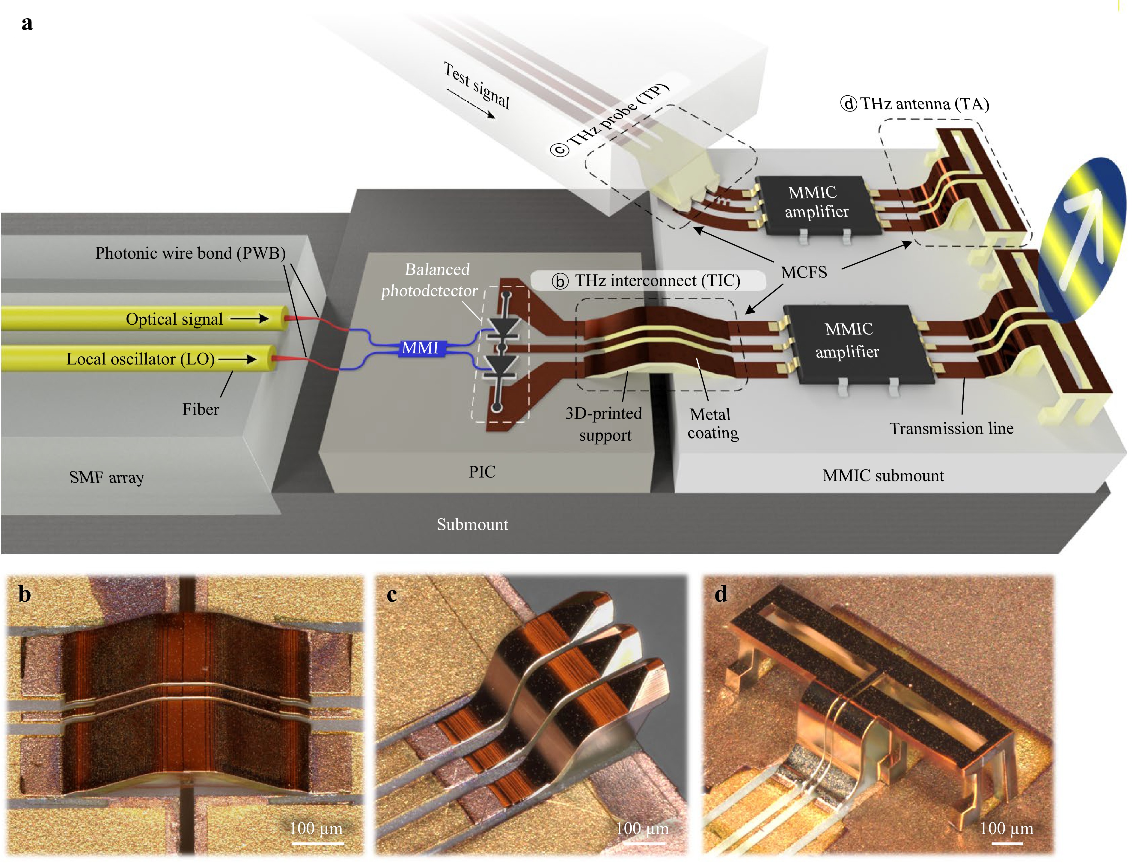
Fig. 1 Concept of a THz system exploiting 3D-printed functional elements based on metal coated freeform structures (MCFS). a The system combines an optoelectronic signal source, relying on a balanced pair of high-speed photodetectors within a photonic integrated circuit (PIC), with a subsequent THz amplifier, that is based on a monolithic microwave integrated circuit (MMIC), and with a THz antenna, that is suspended from the surface of the underlying substrate for efficient emission to the surface-normal direction. The THz chip-chip interconnect between the PIC and MMIC as well as the suspended THz antenna are implemented as metal-coated freeform structures (MCFS). Each MCFS consists of a 3D-printed polymeric support, that is locally coated with metal layers offering high bulk conductivity along with mmW-grade surface quality. The same concept can be used to implement THz probes with unprecedented geometrical design freedom and shape fidelity, lending themselves to testing of mmW and THz integrated circuits, see upper part of the figure. The polymeric support structures of the various MCFS are fabricated using high-resolution multi-photon lithography and can thus be efficiently combined with other 3D-printed functional structures such as photonic wire bonds (PWB) or facet-attached microlenses (FaML). b Micrograph of a THz interconnect (TIC), bridging the gap between coplanar waveguide transmission lines on different THz substrates. c Micrograph of a THz probe (TP) that is turned upside down for better visibility. d Micrograph of a THz antenna (TA) that is suspended from the underlying high-index substrate for increased radiation efficiency.
The fabrication of the MCFS relies on a dedicated multi-step process that is illustrated in Fig. 2. The process steps are shown exemplarily for the fabrication of a TIC, see Fig. 1b, but can also be applied to the other structures shown in Fig. 1. In a first step, two substrates with pre-fabricated planar THz structures such as CPW are coarsely placed to face each other with a gap in-between, see Fig. 2a. As a basis for later directive metal coating, illustrated in Fig. 2d, support and shadowing structures are 3D-printed using in-situ direct-write MPL, see Fig. 2b. The structures are designed to support a metal layer which connects smoothly to the CPW on each substrate and comprise isolation trenches with undercut sidewalls to separate the deposited ground-signal-ground (GSG) metal strips, see Insets ① and ③ in Fig. 2b, d. For protecting the planar THz circuits during global metal deposition, the associated areas on the two substrates are temporarily covered by a poly(methyl methacrylate) (PMMA) film using inkjet printing39, see Fig. 2c. At the transitions between the PMMA-covered planar substrates and the 3D freeform polymeric support, additional 3D-printed shadowing structures are used to prevent short circuits. These shadowing structures, which are shaded in blue in Fig. 2b-e, take the form of multiple arm-like roofs which locally prevent metal deposition, thereby defining isolating regions that separate the metal strips of the GSG transmission line and that seamlessly transition to the isolation trenches of the adjacent 3D support structure. Inset ② in Fig. 2c provides a top view of the left-hand part of the support structure with the corresponding shadowing structures above. The shadowing structures are built upon box-like hollow bases, which act as a flow-stop preventing inkjet-printed PMMA from wetting the entire support structure. In a next step, a highly directed high-vacuum evaporation process is used to deposit metal along a surface-normal direction, see Fig. 2d, thereby forming highly conductive layers on all surfaces with direct line of sight to the evaporation source. More specifically, this step might, e.g., rely on physical vapor deposition (PVD), which offers outstanding directivity along with excellent quality of the deposited layers. For the proof-of-concept demonstration described below, we used an electron-beam PVD system (Univex 400, Leybold GmbH, Cologne, Germany) under standard high-vacuum conditions (pressure approximately 8 × 10⁻⁴ Pa) with samples mounted at a large distance (>60 cm) from the evaporation source. For such large source-to-substrate distances, beam divergences are typically 2°–5°, depending on the crucible size40,41, thereby enabling highly directional deposition on freeform surfaces. We utilized deposition parameters that are compatible with standard wafer-level metallization processes widely used in microfabrication and photonic/electronic device production to ensure scalability of the fabrication processes. After metal coating, the sacrificial PMMA layer is dissolved, thereby lifting off the unwanted metal areas, see Fig. 2e. As a last step, the 3D-printed shadowing structures can be removed mechanically, leaving the final MCFS as shown in Fig. 2f. More details on the processes and the design considerations of the structures can be found in the Materials and Methods Section below and in Supplementary Section 2. Specifically, the width of the signal and ground conductors wS and wG as well as the associated distance dSG of the TIC-based CPW were chosen to provide a desired line impedance of, e.g., 50 Ω along the entire TIC structure. To this end, the dimensions of the 3D-printed freeform support structure and the associated isolation trenches can be continuously varied along the propagation path of the signal, e.g., by smoothly adapting the width of the gaps wgap, which defines the distance dSG between the signal and ground conductors, as a function of the respective height h above the underlying substrate, see Insets ① and ③ in Fig. 2b, d. Details on this adaptation are described in Supplementary Section 2. The metal residues, which are deposited at the ground of the isolation trenches, see Inset ③ in Fig. 2d, do not influence the characteristics of the MCFS-based TIC if the isolation trenches are designed to offer sufficient depth dit.
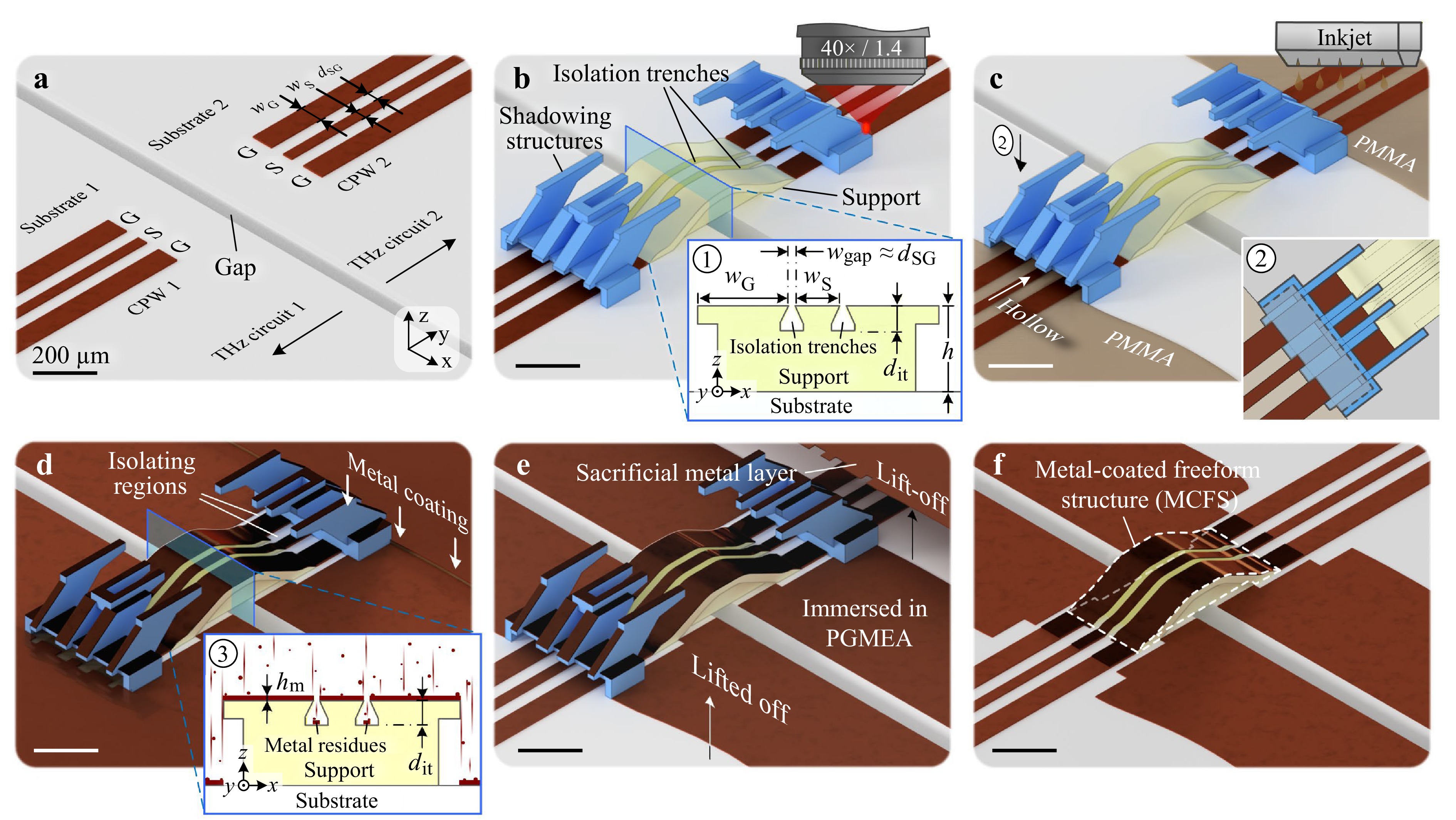
Fig. 2 Fabrication of metal-coated freeform structures (MCFS). The process steps are shown exemplarily for the fabrication of a THz interconnect (TIC) as depicted in Fig. 1b, but also apply to all other structures shown in Fig. 1. All scale bars correspond to 200 µm. a Two substrates with prefabricated planar THz coplanar waveguides (CPW) in ground-signal-ground (GSG) configuration are coarsely placed to face each other with a gap in-between. b Freeform support and shadowing structures are 3D-printed in-situ using multi-photon laser lithography (MPL). The support structures are designed to support metal layers which connect smoothly to the CPW on each substrate. Isolation trenches with undercut sidewalls, see Inset ①, are used to separate the deposited GSG metal strips, see Subfigure d. At the transitions between the planar substrates and the freeform support structures, additional 3D-printed shadowing structures are used to prevent electrical short circuits. These shadowing structures, shaded in blue, take the form of multiple arm-like roofs, which locally prevent metal deposition, thereby defining isolating regions that separate the metal strips of the GSG transmission line and that smoothly transition to the isolation trenches of the adjacent 3D support structure, see Subfigures c and d. c For protecting the planar THz structures during global metal deposition, the remaining areas of the substrates are temporarily covered by a PMMA film using inkjet printing. Inset ② provides a top view on one side of the support structure with the corresponding shadowing structure above. The shadowing structure is built upon a box-like hollow base, which acts as a flow-stop to prevent inkjet-printed PMMA from wetting the entire support structure. d A highly directed evaporation process is used to deposit metal along a surface-normal direction, forming highly conductive layers on all surfaces with direct line of sight to the evaporation source. Isolation of adjacent transmission-line elements is ensured by the isolation trenches with undercut sidewalls, see Inset ③. e After metal deposition, the sacrificial PMMA layer is dissolved, thereby lifting off the unwanted metal areas. f As a last step, the 3D-printed shadowing structures can be removed mechanically, leading to the final MCFS.
It should be noted that the impedance of the transmission line crucially depends on the microscopic features and the exact dimensions of the 3D-printed support structure. More specifically, the width wgap of the gap between the ground and the signal conductor can be as small as 2 µm, and the associated base structure and in particular the undercut sidewalls hence need to be fabricated with sub-micrometer accuracy and resolution to meet the targeted line impedance. This makes the amenability to high-resolution MPL techniques a key feature of our approach. Note also that the 3D-printed polymeric support structures are compatible with the temperature ranges that typically occur during assembly and operation of microelectronic circuits. More specifically, our MPL processes rely on a commercially available photoresist that has previously been used for 3D-printed FaML10, which were demonstrated to maintain their functionality and geometrical integrity at temperatures of 260 °C – a typical number for state-of-the-art reflow soldering processes8. We also measured the dielectric losses of this resist material, finding loss tangents of the order of tan(δ) ≈ 0.02…0.04 in the frequency range between 0.220 THz and 0.325 THz, see Supplementary Section 1. Details on the photoresist can be found in the Materials and Methods Section below.
To verify the high conductivity and surface quality of the deposited metal layers, we analyzed various fabricated MCFS. The surface roughness was measured using a white-light interferometer, revealing a root-mean-square (RMS) surface roughness of Rq,MCFS = (13…14) nm, slightly larger than the roughness of the underlying 3D-printed support of Rq,support = (9…10) nm, see Supplementary Section 3 for further information. The conductivity of the metal films was extracted from four-wire measurements42 of metal strips which were separately fabricated on an oxidized silicon wafer using identical evaporation processes and metal layer stacks, see Materials and Methods Section below. Assuming a homogeneous metal layer, we extract an effective conductivity of σMCFS = (3.29 ± 0.12) × 107 S/m. This corresponds to (57 ± 2)% of the bulk material value of copper according to the International Annealed Copper Standard (IACS, σIACS = 5.8 × 10⁷ S/m) and is consistent with previously reported values using similar deposition techniques43. The slight conductivity reduction compared to ideal bulk material is a known effect related to the grain boundaries of vacuum-deposited metal layers43, which might be mitigated by further process optimization, see Section “RF losses and potential for performance improvement” below for a more detailed discussion.
-
To verify the viability of our concept and to quantify the associated performance parameters, we performed a series of experiments which were geared towards demonstration of the building blocks shown in Fig. 1b-d: THz interconnects (TIC) bridging the gap between transmission lines on different substrates, THz probes (TP) that allow for repeatable contacting of THz circuits, and THz antennas (TA) that are suspended from the underlying high-index substrate for increased radiation efficiency. These experiments are discussed in the following sections.
-
A micrograph of three manufactured TIC connecting three pairs of CPW on two separate alumina substrates is shown in Fig. 3b. For all structures, the CPW endings are separated by LTIC ≈ 0.5 mm and seamlessly connect to the respective TIC, labeled I, II, and III in Fig. 3b. For characterization of the TIC, we first measure the compound S-parameters of the TIC and the associated feed lines, which are contacted using dedicated mmW probes in Plane 1′ and Plane 2′, indicated as blue lines in Fig. 3a. The length of the feed lines between the probes and the TIC amounts to Lfeed = 4 mm. The measured compound S-parameters are exemplarily depicted for TIC II in Fig. 3c, where the blue curve refers to the transmission S2′1′,dB = 10log10(|S2′1′|2) and the green curve to the reflection S1′1′,dB = 10log10(|S1′1′|2). The measurements show excellent agreement with simulations (dashed black lines), see Materials and Methods for details. To remove the influence of the feed lines, the reference planes need to be moved to Plane 1 and Plane 2, indicated as red lines in Fig. 3a, b. To this end, we separately measure the S-parameters of a reference CPW with identical cross section and length Lfeed, which was fabricated on the same substrate. The S-parameters of the reference CPW are then used to de-embed the scattering parameters of the TIC, see Supplementary Section 5 for details. Fig. 3d shows the associated transmission characteristics S21,dB = 10log10(|S21|2) (red lines) for TIC I (upper), TIC II (center) and TIC III (lower), revealing 3 dB-bandwidths of 0.307 THz, more than 0.330 THz and 0.290 THz, respectively. We again performed simulations (dashed black lines), which agree well with the measurements. Note that the measured S-parameters had to be acquired separately in different frequency ranges using dedicated signal sources, waveguides, and probes, thereby leaving a gap between 0.170 THz and 0.200 THz, where no adequate signal sources were available. Note further that the depicted results rely on a de-embedding procedure using the transfer-matrix (T-matrix) approach44 for frequencies up to 0.170 THz, while, for frequencies beyond 0.200 THz, we used a more robust scalar correction that is less prone to error multiplication, but that involves certain approximations, see Supplementary Section 5 for further details on the measurement setup and the de-embedding procedures. To quantify the error introduced by the approximations of the scalar technique and by the unavoidable measurement errors, we performed Monte-Carlo simulations, see Supplementary Section 5 for details. These simulations show that the scalar de-embedding technique provides fairly reliable results also in the presence of unavoidable uncertainties45 associated with S-parameter measurements at frequencies beyond 200 GHz. To the best of our knowledge, the demonstrated 3 dB-bandwidths in excess of 0.33 THz represent a record for in-plane mmW chip-chip connections, e.g., based on advanced metal wire bonds46, and can already well compete with advanced CPW-based flip-chip interfaces47,48. Competing approaches comprise aerosol-jet-printed conductive lines, deposited on dielectric ramps49-52 or epoxy underfills49,53, as well as lithographically defined self-aligning metal nodules, that protrude from the facets of the chips and that require subsequent reflow fusing or electroless plating processes54. However, these approaches have only been demonstrated to work up to 0.22 THz in few cases52,54 and generally lack the precision and design flexibility offered by the presented MCFS concept.
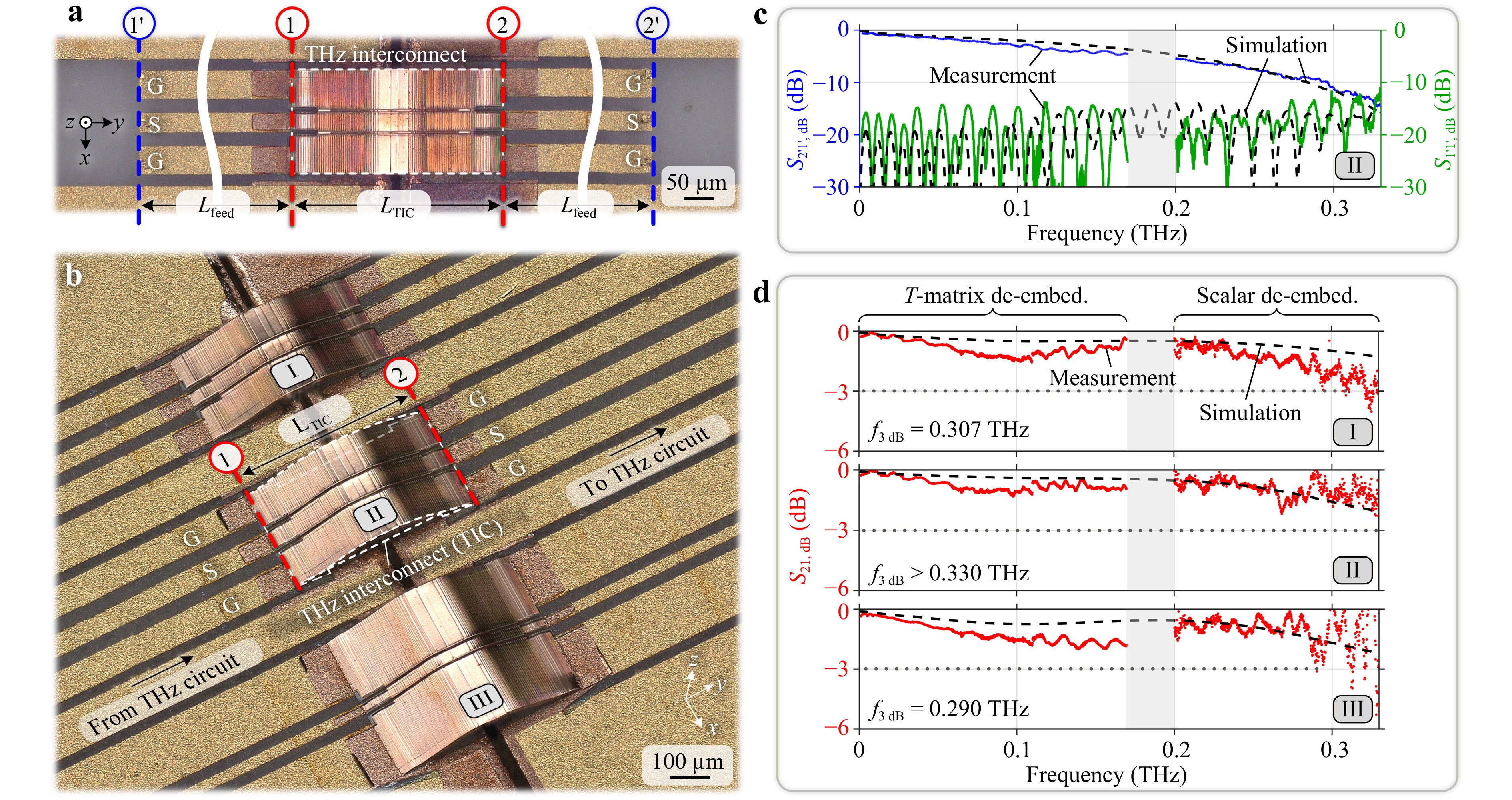
Fig. 3 Characterization of the THz interconnects (TIC). a Top view of a manufactured TIC, seamlessly connecting the ground-signal-ground (GSG) strips of two CPW on two alumina substrates. The CPW endings are separated by LTIC ≈ 0.5 mm, and the length of the feed lines amounts to Lfeed = 4 mm on each side. For characterization of the TIC, we first measure the compound S-parameters of the TIC and the associated feed lines, which are contacted using dedicated probes in Plane 1′ and Plane 2′ (blue lines), see Subfigure c. We then apply a de-embedding procedure to obtain the S-parameters of the TIC only, associated with Plane 1 and Plane 2 (red lines), see Subfigure d. b Micrograph of three manufactured TIC, labeled I, II and III. c Compound S-parameters of TIC II including the associated feed lines. The blue solid curve refers to the measured transmission S2′1′,dB = 10log10(|S2′1′|2) and the green solid curve to the measured reflection S1′1′,dB = 10log10(|S1′1′|2). The measurements show good agreement with a simulation of the associated structure (dashed black lines). d To remove the influence of the feed lines, we measure the S-parameters of a reference CPW on the same substrate and apply de-embedding procedures. The associated transmission characteristics S21,dB = 10log10(|S21|2) (red curves) are shown for TIC I (upper), II (center) and III (lower), revealing 3 dB-bandwidths of 0.307 THz, >0.330 THz and 0.290 THz, respectively. Measurements and simulations (dashed black lines) agree again well. The measured S-parameters are subject to a gap between 0.170 THz and 0.200 THz due to lack of adequate signal sources. For frequencies up to 0.170 THz, a transfer-matrix (T-matrix) approach was used for de-embedding, whereas for frequencies beyond 0.200 THz, the de-embedded S-parameters were estimated using a more robust scalar correction that is less prone to error multiplication, see Supplementary Section 5 for details.
-
We further used the MCFS concept to fabricate broadband TP. The measurement setup for characterization of the TP is shown in Fig. 4a. For the experiment, identical twins of TP (LTP = 415 µm, h = 180 µm) are fabricated on a sample chip at opposite sides of a CPW (Lconn = 3.8 mm). The three tips (pitch 100 µm, contact pad size 20 × 40 µm2) protrude beyond the edges of the sample chip by a distance dedge. A second chip with two short CPW feeds (Lfeed = 1.5 mm) was used for contacting, where the distance between the endings of the CPW are slightly smaller than LTP + Lconn + LTP. A vacuum chuck attached to a manual actuator moves the sample chip in the desired position above the contacting chip. With the sample chip in contact, S-parameters between Plane 1′′ and Plane 2′′, indicated by brown lines in Fig. 4a, are measured. Using again dedicated de-embedding procedures, the reference planes are first moved to Plane 1′ and Plane 2′, corresponding to the blue lines in Fig. 4a, see Supplementary Section 6 and associated Fig. S8 for details. In a second step, we move the reference planes to Plane 1 and Plane 2, indicated by red lines in Fig. 4a, thereby estimating the characteristics of a single TP–the associated transmission factor S21,dB = 10log10(|S21|2) is shown in Fig. 4b. The 3 dB-bandwidth amounts to 0.192 THz, and the 6 dB-bandwidth is far beyond the 0.330 THz range of our measurement system. Measurement and simulation (dashed black line) are again in good agreement. We attribute the slight deviations above 0.1 THz to the probes used to connect the contacting chip to our measurement equipment. Specifically, these probes are intended for wafer-level measurements with surface qualities superior to the comparatively rough gold strips of the CPW feeds on our test substrates. More details on the measurement setup and the de-embedding procedures are given in Supplementary Section 6. To the best of our knowledge, the demonstrated 3 dB-bandwidths in excess of 0.19 THz represent a record for additively manufactured electrical probes. Previous demonstrations were limited to the (75–110) GHz frequency band with insertion losses of the order of 1 dB per probe55.
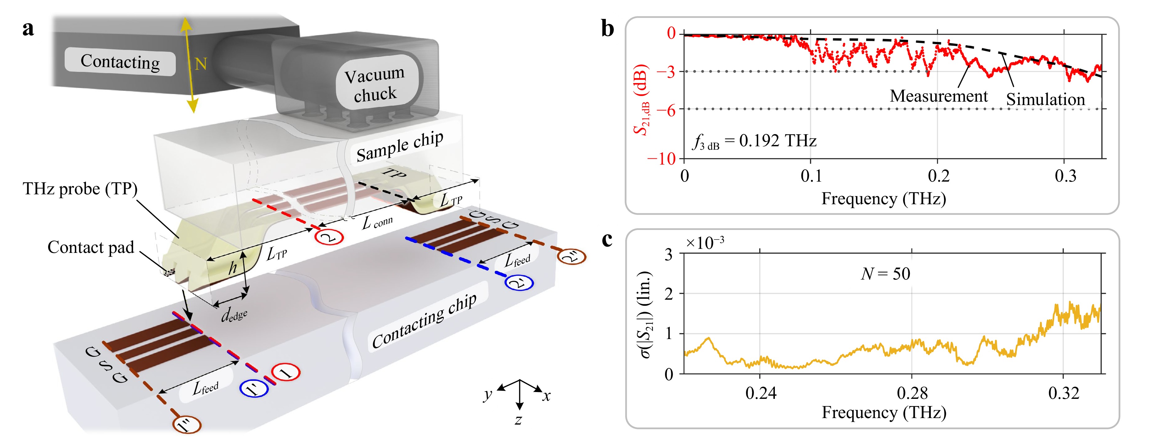
Fig. 4 Characterization of the THz probes (TP). a Identical twins of TP (LTP = 415 µm, h = 180 µm) are fabricated on a sample chip at opposite ends of a CPW (Lconn = 3.8 mm). The three tips (pitch 100 µm) are designed for a contact pad size of 20 × 40 µm2 or more and protrude beyond the edges of the sample chip by a distance dedge. A second chip with two short CPW feeds (Lfeed = 1.5 mm) was used for contacting (contacting chip), where the distance between the endings of the CPW are slightly smaller than LTP + Lconn + LTP. A vacuum chuck attached to a manual actuator is used to move the sample chip in the desired position above the contacting chip. With the sample chip in contact, S-parameters between Plane 1′′ and Plane 2′′ (brown lines) are measured. Using dedicated de-embedding procedures, the reference planes are first moved to Plane 1′ and Plane 2′ (blue lines) and then to Plane 1 and Plane 2 (red lines), thereby extracting the characteristics of a single TP, see Supplementary Section 6 for details. b Estimated transmission characteristics S21,dB = 10log10(|S21|2) of a single TP. The 3 dB-bandwidth amounts to 0.192 THz, and the 6 dB-bandwidth is far beyond the 0.330 THz range of our measurement system. Measurement and simulation (dashed black line) are again in good agreement. c To further demonstrate the robustness of our probes and to verify the repeatability of the connections, we repeat our measurement N = 50 times, detaching and re-establishing the contact between the sample and the contacting chip after each repetition. From the resulting data, we extract the standard deviation of the magnitude of the complex-valued amplitude transmission factor S21 as a function of frequency. We find a remarkably low maximum standard deviation of σ(|S21|)max of approximately 2 × 10⁻³ near 0.32 THz, corresponding to –55 dB.
To further demonstrate the robustness of our probes and to verify the repeatability of the connection, we repeat our measurement N = 50 times, detaching and re-establishing the contact between the sample and the contacting chip after each repetition. From the resulting data, we extract the standard deviation of the magnitude of the complex-valued amplitude transmission factor S21 as a function of frequency, see Fig. 4c. We find a remarkably low maximum standard deviation of σ(|S21|)max ≈ 2 × 10⁻³ near 0.32 THz, corresponding to –55 dB. These results are already on par with conventional commercially available probes fabricated via conventional micromachining techniques where, e.g., standard deviations σ(|S21|) in the range (–60…–43) dB have been demonstrated for 2 mm-long CPW in the 0.3 THz band56.
-
As a last implementation example, we explore TA. A schematic of a manufactured TA operating at frequencies around 0.28 THz is shown in Fig. 5a. Connecting to the CPW feed (Lfeed = 1.1 mm), the 3D-printed support structure provides a mechanical base for guiding the signal and the ground conductors of the CPW away from the substrate to form an elevated slot antenna for improved radiation into the upper half-space. The antenna comprises two slots, each having a width of wslot = 60 µm and a length of Lslot = 400 µm, equivalent to approximately half the guided wavelength at the targeted radiation frequency of 0.28 THz. The height of the structure (h = 250 µm) was adapted such that the evaporated metal on the substrate simultaneously acts as a reflector. The radiation pattern for different elevation angles θ is shown in Fig. 5b, where the solid blue line represents the experimentally measured co-polarized component of the realized gain GR,TA,dBi(θ) = 10log10GR,TA(θ) in the upper half-space region (H-plane), while the dashed black line represents the simulation. The measurement and the simulation are in good agreement, given the general challenges associated with accurately measuring radiation patterns of on-chip antennas at elevated frequencies of hundreds of GHz57–59. A maximum realized gain of 5.5 dBi was measured perpendicular to the substrate near 0.274 THz, in good agreement with the simulation. Note that conclusive measurement data could only be obtained for the co-polarization component of the realized gain in the H-plane, see Supplementary Section 7 for a more detailed discussion. To still provide a complete picture of the antenna’s far-field behavior, simulation results including the co- and cross-polarization components for both the H- and the E-planes are given in Supplementary Figure S10 and the associated discussion, along with details on the measurement setup and the characterization. To the best of our knowledge, our experiments represent the first demonstration of an additively manufactured 3D freeform mmW or THz antenna which does not require any manual assembly steps. Previous approaches have either been limited to the fabrication of bulky stand-alone horn antennas32,33 or are based on aerosol-jet-printed conductive structures on the surface of non-planar dielectric substrates60, often requiring additional mechanical assembly steps to yield functional devices32,60. While the reported antenna gain of 5.5 dBi is already comparable61–64 to the best values of 6…9 dBi that have been obtained for highly optimized comb-shaped dipoles with chip-integrated dielectric resonators62, our approach clearly leaves room for further improvement. Specifically, our MCFS-based antennas are fully compatible with aperture enhancement through multi-element arrays65, dielectric superstrates or microlenses66, or local patterning of, e.g., metamaterial rings or surface-wave suppression structures around the on-chip antenna61,67. Combining MCFS with such approaches represents a promising route towards high-performance THz transmitters for wireless links36.
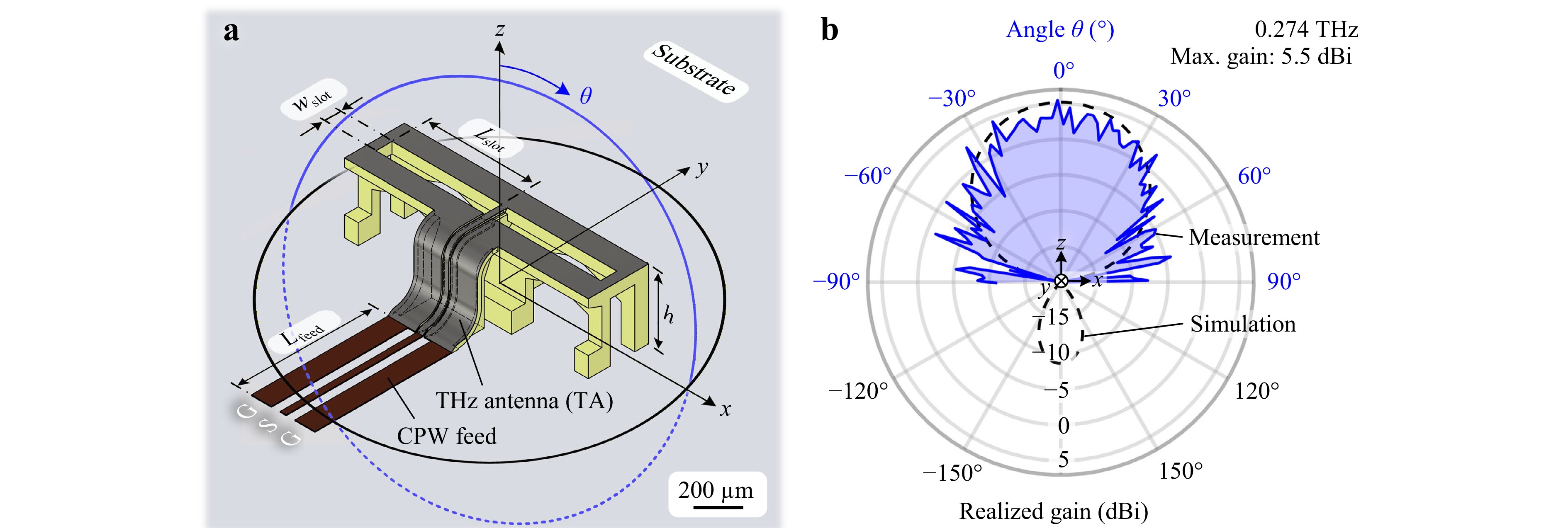
Fig. 5 Characterization of the THz antennas (TA). a Schematic of the manufactured TA operating at a frequency centered around 0.28 THz. Connecting to the CPW feed (Lfeed = 1.1 mm), the 3D-printed support structure provides a mechanical base for guiding the signal and ground conductors of the CPW away from the substrate to form an elevated slot antenna for improved radiation to the top. The antenna comprises two slots, each having a width of wslot = 60 µm and a length of Lslot = 400 µm, equivalent to approximately half the guided wavelength at the targeted radiation frequency of 0.28 THz. The height of the support structure (h = 250 µm) was adapted such that the evaporated metal on the substrate simultaneously acts as a reflector. b Measured radiation pattern for different elevation angles θ, where the solid blue line represents the co-polarized component of the realized gain GR,TA,dBi(θ) = 10log10GR,TA(θ) in the upper half-space region (H-plane). A maximum realized gain of 5.5 dBi was measured perpendicular to the substrate near 0.274 THz, in good agreement with the simulation (black dashed line).
-
Electrical conductivity of metal layers is a key determinant of RF losses in THz structures, as reduced conductivity directly increases ohmic attenuation and thereby degrades device performance. Although the measured effective conductivity of our metal structures corresponding to (57 ± 2)% of the bulk material value of copper is already on par with previously reported values obtained by vacuum deposition techniques43, several refinement pathways exist. First, optimizing seed-layer conditions, e.g., by lowering the background gas pressure, increasing the substrate temperature, and/or reducing the deposition rate can improve nucleation, reduce porosity, and yield smoother films with larger grain sizes, for which scattering from grain boundaries and surface roughness is further reduced68. Moreover, post-deposition thermal annealing in inert or forming-gas atmospheres at temperatures in the range (150…350) °C is known to promote grain growth and to reduce defects. More specifically, resistivity reductions by (20…30)% are commonly reported for sputtered Cu films after annealing68, reaching conductivities of more than 95% of the International Annealed Copper Standard (IACS) benchmark (σIACS = 5.8 × 10⁷ S/m)69. For polymer-based templates that are more sensitive to elevated temperatures, localized post-processing such as nanosecond pulsed-laser annealing or flash-lamp annealing can induce near-surface recrystallization and enlarge grains from the sub-micrometer to the micrometer range70,71, thereby reducing resistivity by approximately (30…40)%. Finally, increasing the overall thickness of the metal layer, for example by combining an optimized seed layer with subsequent electroplating, helps mitigating thin-film scattering effects. Specifically, electroplated copper layers with a thickness in the µm-range have been reported to approach bulk-like resistivity levels, enabled by improved grain growth and surface continuity72. However, it should also be noted that the rather small THz interconnects, probes, and antennas shown in our work can still achieve outstanding performance, even if the deposited metal layers do not reach the full conductivity levels of ideal bulk copper. To quantify the influence of the metal-layer conductivity on the performance of our MCFS, we exemplarily simulate the transmission of the second THz interconnect (TIC II) with varying conductivity levels, see Supplementary Section 4 for details. We find that the current device performance could only be improved by less than 0.1 dB when approaching bulk material values according to 100% of the ideal IACS benchmark (σIACS = 5.8 × 10⁷ S/m), while a conductivity equivalent to only 10% of the IACS standard would still be sufficient to keep the simulated transmission loss below 1 dB up to 230 GHz with 3 dB-bandwidths only slightly reducing. Note that these levels of conductivity can also be reached with other materials that are widely established in microfabrication, comprising, e.g., aluminum (Al) reaching approximately 61% of the IACS conductivity benchmark (σAl = 0.61 σIACS), gold (Au, σAu = 0.70 σIACS), silver (Ag, σAg = 1.05 σIACS), or nickel (Ni, σNi = 0.25 σIACS). Our approach is hence not limited to copper and leaves significant freedom to select the material according to application-specific needs such as corrosion resistance or bio-compatibility. The choice of copper for our current proof-of-concept experiments was primarily motivated by its wide availability, low cost, and well-studied electrical properties as well as by the fact that it is readily available through established PVD processes in many microfabrication facilities.
-
Accelerating the underlying 3D printing technique and increasing the write field size are key to bringing the presented concept to industrial applications. Several established strategies exist that could enhance printing speed while maintaining sub-micrometer resolution. A first route relies on synchronizing the movement of the galvanometric scanning mirror to the movement of the sample stage. By avoiding stop/start overhead and enabling continuous scanning without idle times through stage movement and beam relocation, such approaches can provide a two- to tenfold increase in throughput for MPL structuring73,74. A second option exploits multi-beam or multi-focus parallelization, in which a high-power femtosecond laser beam is divided into tens to thousands of individually addressable foci using spatial light modulators, micro- or meta-lens arrays, or digital micromirror devices (DMD)75–77. This method allows to scale writing speeds approximately linearly with the number of foci, and throughput gains by factors of 10 to 300 have been demonstrated with recent experiments involving more than 120,000 cooperative focal spots77. A third class of concepts involves drum-scanner architectures, in which the substrate is mounted on a rotating drum enabling continuous, high-speed scanning along one axis. While opto-mechanically more demanding, particularly when maintaining high-NA focusing on moving or curved surfaces, drum-scanner based systems could offer strong benefits for long, repetitive patterns or continuous substrates. Finally, projection-based 3D-printing approaches could be combined with MPL in a hybrid approach, using, e.g., rapid exposure of thick layers parallel to the substrate plane through projection micro-stereolithography (PµSL) to fabricate large bulky features while resorting to MPL only for sub-micrometer regions or surface elements that are subject to stringent limitations of roughness. The volumetric throughput of PµSL can exceed that of point-by-point MPL by factors of 102 to 104 for bulky features78, offering an attractive path for mixed-resolution devices. Note that single-photon PµSL alone, while offering outstanding throughput, does not provide the required resolution, see next Section. Regarding the cost-performance trade-off, strategies based on synchronizing the galvanometric scanning mirror to the movement of the sample stage could be readily implemented, but might only offer a limited gain in throughput of up to an order of magnitude, whereas multi-beam and hybrid projection-based methods offer significantly higher throughput, but require novel printer architectures that are currently not commercially available. Considering volumetric printing speeds of commercially available MPL systems79,80 and assuming a realistic 10× increase in throughput would already enable fabrication times below 10 s for the TIC, TP or TA demonstrated in this work, highlighting the commercial potential of the MCFS approach.
Another important aspect for practical viability of the presented fabrication approach is the achievable reproducibility and yield. So far, only a small number of devices has been fabricated and characterized, such that it is not yet possible to provide statistically meaningful yield values. Still, the results obtained so far indicate decent robustness and reproducibility of the underlying fabrication processes. As an example, we fabricated three nominally identical THz antennas and measured the associated gain levels in the surface-normal direction for different frequencies. We found maximum gain levels of 5.0, 5.2 and 5.5 dBi for frequencies of 273.9, 273.9 and 273.6 GHz, respectively, showing a good level of reproducibility. From a more fundamental viewpoint, the underlying additive manufacturing approach based on MPL is a well-established and highly reproducible microfabrication technique, and its suitability for scalable manufacturing has been demonstrated in the context of 3D-printed coupling elements for optical chip-chip connections based on photonic wire bonds (PWB)4,8 or facet attached microlenses (FaML)10. Early demonstrations4 have, e.g., relied on fabricating and characterizing arrays of 3D-printed PWBs, showing standard deviations of the reported optical loss of only 0.15 dB. This analysis has been complemented by a recent study8 of production-grade PWBs and FaMLs with low optical loss, high reproducibility and long-term stability, reporting scalable manufacturing with yields of close to 100%. These demonstrations show that MPL can meet industrial reliability and yield requirements even for functional optical components which are much more sensitive to alignment inaccuracies and shape deviations than the THz components demonstrated in our current work. The PVD-based addition of the metal coating is an industrially established and widely used microfabrication technique that has been advanced to provide highest uniformity on extended areas and that should not introduce additional yield penalties. We are hence confident that our approach can offer a path towards scalable high-yield fabrication of functional THz components based on MCFS, in particular when producing larger batches on an industrial scale.
-
In recent years, low-cost projection-based single-photon lithography methods such as projection micro-stereolithography (PµSL) have also gained interest for fabricating THz devices81,82. The key difference to the multi-photon-lithography approaches presented in our manuscript is the achievable resolution. More specifically, single-photon printing processes are typically limited to rather large layer thicknesses, as dictated by the depth of cure. For specifically optimized resin formulations and exposure conditions83, these layer thicknesses can reach down to 3 µm, but typically they are rather in the range of (10…50) µm for practical use cases related to THz components82. Similar restrictions apply to the achievable lateral resolution, which is reported to be approximately 1 µm for specific positive features such as suspended single-pixel lines84, while reproducible fabrication of negative features such as gaps only works well for widths of multiple pixels85, typically exceeding 5 µm. These limitations have restricted the use of PµSL mainly to fabrication of rather bulky stand-alone THz components such as hollow-core waveguides31 and horn antennas32,33 which typically require additional mechanical assembly steps for integration into more complex systems32. Some experiments have also explored in-situ printing of PµSL-based THz components on functional substrates57, but decent performance was only obtained in case of structures with planar surfaces parallel to the substrate, while structures involving 3D freeform surfaces showed a clear degradation in structural fidelity and functional performance. This is in sharp contrast to the THz interconnects, probes, and suspended antennas demonstrated in our work, which crucially rely on smooth 3D freeform surfaces, fully suspended three-dimensional geometries, and air gaps of approximately 2 µm with undercut sidewalls to achieve proper impedance matching and high device performance. These requirements can currently only be met by the MPL-based printing approaches, offering voxel heights and associated layer thicknesses and lateral feature sizes below 500 nm both for lines and gaps86. The outstanding resolution along with the ability to produce 3D freeform surfaces with ultra-low roughness below 10 nm, see Section 3 of the Supplementary Information, is key to the advanced on-chip structures shown in our manuscript.
-
We have introduced a novel concept for fabricating precisely defined mmW and THz structures, relying on in-situ printing of freeform polymer support structures that are selectively coated through highly directive metal deposition techniques. The resulting metal-coated freeform structures (MCFS) offer high surface quality in combination with conductivities comparable to bulk material values and do not require any manual assembly steps. The viability of the approach is shown in a series of proof-of-concept experiments. In a first set of experiments, we show THz interconnects (TIC) that bridge the gap between transmission lines located on different substrates and that offer 3 dB-bandwidths exceeding 0.33 THz. In a second set of experiments, we demonstrate that the vast design freedom offered by our fabrication technique can be leveraged for cost-effective THz probes (TP) that allow highly repeatable contacting over many probing cycles. Our TP offer 3 dB-bandwidths exceeding 0.19 THz and 6 dB-bandwidths far beyond the 0.33 THz range of our measurement system. A third set of experiments is finally dedicated to THz antennas (TA), which are suspended from the underlying high-index substrate for better radiation efficiency. At a frequency of 0.27 THz, a maximum realized gain of 5.5 dBi in the direction perpendicular to the substrate is measured. Our proof-of-principle experiments show the vast potential of the proposed fabrication technique, and the demonstrated structures already offer unique performance parameters such as record-high bandwidths for in-plane mmW chip-chip connections and for additively manufactured probes. Our concept offers unprecedented design freedom, does not rely on expensive high-precision assembly steps, and is widely applicable to a rich variety of use cases, thereby paving a path towards advanced mmW and THz systems in communications36, sensing37, or ultra-broadband signal processing38.
-
The substrates used as the base for the subsequent fabrication steps have a total size of 100 mm × 100 mm each and consist of a 635 μm-thick alumina (Al2O3) layer with a single-sided gold coating (Reinhardt Microtech GmbH, Ulm, Germany) and a thin titanium adhesion layer in-between. The Al2O3 layer exhibits a relative permittivity of ε′ = 9.9 and a loss tangent of tan(δ) = 1 × 10⁻⁴, both specified at a frequency of 1 MHz. The gold metallization has a thickness of 3 μm with a specified variance of ±30%, and a root-mean-square (RMS) surface roughness of Rq,gold = (121…129) nm was measured using a white-light interferometer, see Supplementary Section 3 for further information. For achieving a characteristic CPW impedance of 50 Ω, different combinations of the signal conductor width wS, ground conductor width wG and signal-to-ground conductor distance dSG were chosen, see Supplementary Section 2. All CPW designs facilitate contacting with GSG probes with pitches of 100 µm for compatibility with existing measurement equipment.
The transmission lines used in the experiments for the TIC and TA were structured into the gold layer using a wet etching process. To this end, a 1.5 μm-thick layer of positive-tone photoresist (AZ 1505, Microchemicals GmbH, Ulm, Germany) was first spin coated on the substrates and subsequently baked at a temperature of 95°C for five minutes. The resist was then structured using a direct-write laser lithography tool (DWL 66fs, Heidelberg Instruments Mikrotechnik GmbH, Heidelberg, Germany) and developed (AZ 400K 1:4, Microchemicals GmbH). To strip the metal in the uncoated regions, wet etching is performed with potassium iodide and titanium-tungsten etchants. Due to the significant variation of the metallization thickness across the substrate, over- and underetching of the metal structures was hardly avoidable. As a result, wS and wG were generally found to be decreased, while dSG was increased compared to the original design. The dimensions of the fabricated CPW are indicated in Table 1 and show fair agreement with the design values. From simulations, the characteristic impedance is expected to be in the range (58…60) Ω. The deviations from the targeted 50 Ω can be reduced by an optimized fabrication process, relying on gold layers with better thickness uniformity, which would further improve the impedance matching and hence the performance of our MCFS-based THz structures.
Experiment L (mm) wS (µm) wG (µm) dSG (µm) TIC I 4.0 45 65 30 TIC II 4.0 56 72 35 TIC III 4.0 30 150 30 TP 1.5 / 3.8 / 6.8 61 79 29 TA 1.1 22 89 16 Table 1. Overview of dimensions of manufactured CPW.
In contrast to this, the transmission lines used in the experiments for the TP were structured into the gold layer using a commercially available laser ablation system (ProtoLaser R4, LPKF Laser & Electronics SE, Garbsen, Germany), equipped with a 515 nm picosecond laser with a typical beam diameter of 15 µm. We used 1.5 ps-wide pulses with 24 µJ pulse energy at repetition rates between 150 kHz and 300 kHz for structuring the substrates. The dimensions of the fabricated CPW are again listed in Table 1 and show good agreement with the design values. The characteristic impedance is expected to be approximately 55 Ω.
-
After structuring the CPW, a wafer saw was used for cutting the alumina substrates into individual chips. For easier handling, the individual chips were temporarily fixed to glass cover slides using UV glue (NOA 61, Norland Optical Adhesive Inc., Jamesburg, USA). For the experiments with the TIC, see Fig. 3, the ends of the 4 mm-long CPW feeds are approximately 230 µm away from the diced chip edges, keeping the length of the bridging TIC (LTIC ≈ 0.5 mm) manageable when the CPW are placed facing each other. The gap between the two substrates was roughly 40 µm wide. The sample chip used in the TP experiments, see zoom-in in Supplementary Fig. S7, is roughly 4.4 mm wide and 8.8 mm long to provide sufficient area for pick-up with a custom vacuum tool (3.5 mm × 8 mm). The connecting CPW (Lconn = 3.8 mm) between the two TP ends approximately 320 µm away from the diced chip edge on each side. This leaves enough room for a smooth routing of the signal and ground conductors, while ensuring that the tips of the TP protrude beyond the edges of the chip by a sufficient distance dedge for better visibility via the top-view camera used in the experimental setup illustrated in Supplementary Fig. S7. In the areas between the ends of the transmission lines and the chip edge, the gold was removed from the alumina substrates for more reliable height detection during MPL structure and for better adhesion of the 3D-printed support structures, see next paragraph. Similarly, for the TA as shown in Fig. 5, the metal layer was removed from the surface of the substrate in a 250 µm-long region following each end of the transmission line. The remainder of the gold layer was maintained to act as a reflector for the suspended TA.
-
The 3D-printed support and shadowing structures, see Fig. 1b-d, were fabricated using an in-house-built MPL system with a 40×/1.4 objective (PlanApochromat Oil DIC M27, Carl Zeiss Microscopy GmbH, Oberkochen, Germany), galvanometer-actuated mirrors, and a 780 nm femtosecond laser with a repetition rate of 80 MHz and a pulse width of 58 fs (C-Fiber 780 HP, Menlo Systems GmbH, Planegg, Germany). The samples were mounted in the lithography machine along with the associated glass cover slides, and the objective approaches the samples along the negative z-direction, see Figs. 3-5. For lithographic structuring, we use a commercially available acrylate-based photoresist (VanCore B, Vanguard Automation GmbH, Karlsruhe, Germany), for which the dielectric response was independently measured, see Supplementary Section 1. All structures are printed to the substrates with the axis of the lithography beam perpendicular to the surface of the chips, i.e., along the z-direction, see Figs. 3-5. We use automated procedures for detecting the substrate surface with sub-100 nm precision. Where possible, the underlying metal layer was removed to avoid scattering of the laser beam due to the roughness of the gold layer. For lateral alignment, we relied on the camera-based vision system of our lithography setup, which leads to a lateral alignment precision that is also of the order of 100 nm. Due to the limited write field in our current lithography setup, corresponding approximately to a circle with a diameter of 400 µm, the support and shadowing structures are printed in separate steps, and larger support structures such as those of the TIC and TA are split into two and three parts, respectively, which are printed one after another. Proper alignment of the separately printed models is ensured by a defined translation of the underlying chip using a precision stage in the lithography system. To reduce the required fabrication time, all structures are printed with a standard layer-to-layer distance (slicing distance) of 100 nm only for the outermost shell, whereas the inside of the structures is filled with a coarser spacing of 600 nm. All structures were printed using a voxel scanning speed of up to 50 mm/s with an estimated average optical power of 31 mW being emitted from the lithography objective into the resist. After printing, unexposed photoresist is removed in a two-step development process using propylene-glycol-methyl-ether-acetate (PGMEA) as a developer for 15 minutes, followed by rinsing in isopropyl alcohol (2-propanol).
-
For protecting the planar THz structures during the global metal deposition, see Fig. 2c, e, we used an inkjet-printed poly(methyl methacrylate) (PMMA) layer, which was later removed by propylene-glycol-methyl-ether-acetate (PGMEA). Since PGMEA is also used in the development process of the 3D-printed structures, see Materials and Methods Section above, deterioration of the 3D-printed support structures during the PMMA lift-off is not to be expected. For the ink preparation, PMMA with an average molecular mass of 1.5 × 10⁴ daltons (Sigma-Aldrich Inc., Saint Louis, USA) was dissolved in 1,3-dimethoxybenzene (≥98%, Sigma-Aldrich Inc.) to achieve a concentration of 80 g/L. We further added 5% hexylbenzene (97%, Sigma-Aldrich Inc.) to mitigate the so-called coffee-ring effect87. Finally, the ink was filtered using polytetrafluoroethylene (PTFE) filters (pore size 200 nm) before being filled in the cartridges (FUJIFILM Dimatix Inc., Santa Clara, USA) of the inkjet printer (PiXDRO LP50, SÜSS MicroTec SE, Garching, Germany). The substrate and printhead temperatures were set to 50°C and 27°C, respectively. The built-in camera system of the printer was used to align the printing region with respect to the CPW and the shadowing structures on the chips. For all samples, the transmission lines are covered over their full length up to the flow-stop that is part of the 3D-printed shadowing structure, see Fig. 2c. To achieve sufficient coverage, a minimum of five layers were printed using a resolution of 550 dpi.
-
For applying the highly-directive metal coating, see Fig. 2d, an electron-beam physical vapor deposition (PVD) process is used (Univex 400, Leybold GmbH, Cologne, Germany) at a pressure of 8 × 10⁻⁴ Pa. The sample chips are mounted with a large distance (>60 cm) above the evaporation source to ensure a small divergence of the vapor flow. For such large source-to-substrate distances, beam divergences are typically 2°–5°, depending on the crucible size40,41. The mounting plate carrying the samples can further be tilted in one direction and rotated around an axis that is normal to the mounting surface to improve the uniformity of the deposited layers. For the coating of the TIC and TP, the direction of evaporation is perpendicular to the substrates, i.e., along the negative z-direction in Figs. 2-4. For the TA in Fig. 5, the direction of deposition is set to an angle of 45° with respect to the negative z-direction in the (y,z)-plane, i.e., the deposition is done along the (0,1,-1)-direction of the coordinate system shown in Fig. 5a, which permits coating of the support structure also in the ramp-like sections which are partially perpendicular to the substrate. The deposited layer stack comprises a sequence of different metals: First, a 5 nm-thick adhesion film of titanium is applied, followed by the main layer consisting of 300 nm copper. Afterwards, a 5 nm titanium layer is deposited to act as a diffusion barrier between the copper and the final 10 nm-thick gold passivation layer. For the TIC and TA, the process is repeated twice for a total thickness of the metal coating of hm = 0.64 µm. For the TP, the initial titanium adhesion layer was replaced by a 30 nm aluminum coating, leading to a layer stack with a thickness of 345 nm. The process is repeated four times for a total metal thickness of hm = 1.38 µm for the TP. This ensures that the thickness of the metal coating is always a multiple of the skin depth at the targeted operation frequency. The quality of the deposited metal layers in PVD is further influenced by several process parameters. High vacuum reduces scattering and allows ballistic trajectories of the evaporated atoms, which improves uniformity and film density. Substrate rotation and tilt further enhance layer homogeneity across non-planar surfaces. The deposition rate and the choice of adhesion/diffusion layers can control roughness, continuity, and long-term stability of the metal films. The deposition parameters used in our processes are consistent with standard wafer-level metallization processes widely used in microfabrication and photonic/electronic device production and should hence pave a path towards a scalable fabrication that can rely on established industry-standard processes. For estimating the conductivity of our metal films, multiple metal strips with a length of 2 mm and widths of 10 µm and 15 µm were fabricated on a silicon wafer, covered by a 1 µm-thick silicon dioxide isolating layer. We use identical evaporation parameters as for the MCFS and repeat the process twice for achieving a metal layer stack with a thickness which was measured to be hm ≈ 590 nm using a profilometer (Tencor P-7, KLA Inc., Milpitas, USA). From four-wire measurements42 using a precision source/measurement unit (B2902A, Keysight Technologies Inc., Santa Rosa, USA), we extract an effective sheet resistance of RS,MCFS = (21.6 ± 1.9) mΩ/sq, corresponding to an effective conductivity of σMCFS = 1/(hmRS,MCFS) = (3.29 ± 0.12) × 107 S/m. To mitigate offset errors originating from thermal electromotive forces, measurements were carried out for both polarities of the driving current, considering the average of the two associated voltage readings (reverse current method)42.
-
The transmission and reflection characteristics of the TIC, see Fig. 3c, d, the TP, see Fig. 4b, as well as the far-field characteristics of the TA, see Fig. 5b, are simulated using a commercially available numerical time-domain solver (CST Microwave Studio, Dassault Systèmes SE, Vélizy-Villacoublay, France). The alumina substrate is modeled using the manufacturer specifications of the relative permittivity and loss tangent, see paragraph on “CPW design and fabrication” above. The CPW are simulated using the “lossy metal” option of CST Microwave Studio, which models the penetration of electromagnetic fields inside a very good, but still imperfect conductor by means of an internal one-dimensional surface-impedance model88. This model allows to account for the skin effect without further mesh refinement. We also include the measured RMS surface roughness Rq,gold of the gold layer of the respective assembly, see above. This value is used as an input for the so-called gradient model provided within CST Microwave Studio, which accounts for the increased total loss and inner inductance effects that occur as a consequence of the rough surface88. The material characteristics of the 3D-printed support structures are modeled using the results of the dielectric response measurement of the underlying photoresist, see Supplementary Section 1. To this end, the measured values for the permittivity ε′ and loss tangent tan(δ) in the frequency range from 0.220 THz to 0.325 THz were imported into CST Microwave Studio and fitted using a dispersion model of first order. Another crucial aspect is the correct representation of the comparatively small isolation trenches inside the 3D-printed support structures, separating the deposited metal layers by a gap of the order of a few micrometers. In the simulation of transmission lines and THz devices with dimensions up to the mm-range, a detailed representation of the field within these gaps and metal layers would lead to an unrealistic number of mesh cells that cannot be handled with the available computing resources. We therefore use a locally refined mesh inside the gaps in combination with the “thin panel” option of CST Microwave Studio, which relates the tangential electric and magnetic fields on the surface of the extended metal strips with the help of surface impedances88. Furthermore, the TA is simulated with open boundaries in combination with a so-called multilayer background to emulate an infinitely extended substrate. Using this approach, any reflections at the lateral edges of the substrate can be avoided, albeit the restricted simulation volume.
-
The micrographs in Fig. 1b-d and in Fig. 3b were created using a digital microscope (VHX-7000, Keyence Ltd., Osaka, Japan) with a tiltable and motorized imaging head comprising a CMOS camera (VHX-7100, Keyence Ltd.). Magnifications of 300× and 150× were used for the micrographs in Fig. 1b, c and Fig. 1d, respectively, and the micrograph in Fig. 3b was taken at a magnification of 80×. In all cases, the microscope was set to acquire large image stacks (~50–100 images) with different focus distances, which were then combined into focus-stacked images using a commercially available software (Helicon Focus, Helicon Soft Ltd., Kharkiv, Ukraine).
-
This work was supported by the Deutsche Forschungsgemeinschaft (DFG, German Research Foundation) via the Excellence Cluster 3D Matter Made to Order (EXC-2082/1–390761711), via the DFG Collaborative Research Center HyPERION (SFB 1527), and via the projects PACE (#403188360) and GOSPEL (#403187440) within the Priority Programme “Electronic-Photonic Integrated Systems for Ultrafast Signal Processing” (SPP 2111), by the ERC Consolidator Grant TeraSHAPE (#773248), by the EU Horizon 2020 project TeraSlice (#863322), by the European Innovation Council (EIC) transition project HDLN (#101113260), by the BMBF project Open6GHub (#16KISK010), by the Alfried Krupp von Bohlen und Halbach Foundation, and by the Karlsruhe School of Optics & Photonics (KSOP).
Freeform terahertz structures fabricated by multi-photon lithography and metal coating
- Light: Advanced Manufacturing , Article number: 36 (2026)
- Received: 15 June 2025
- Revised: 07 March 2026
- Accepted: 10 March 2026 Published online: 06 May 2026
doi: https://doi.org/10.37188/lam.2026.036
Abstract: Direct-write multi-photon laser lithography (MPL) combines highest resolution on the nanoscale with essentially unlimited 3D design freedom. The groundbreaking potential of this technique has been demonstrated in various application fields, including micromechanics, material sciences, microfluidics, life sciences, as well as photonics, where in-situ printed optical coupling elements offer new perspectives for package-level system integration. However, millimeter-wave (mmW) and terahertz (THz) devices did not yet leverage the unique strengths of MPL, even though the underlying devices and structures could also greatly benefit from 3D freeform microfabrication. A key challenge is that functional mmW and THz structures require materials with high electrical conductivity and low dielectric losses, which are not amenable to structuring by multi-photon polymerization. In this work, we introduce and experimentally demonstrate a novel approach that leverages MPL for fabricating high-performance mmW and THz structures with hitherto unachieved functionalities. Our concept exploits in-situ printed polymer templates that are selectively coated through highly directive metal deposition techniques in combination with precisely aligned 3D-printed shadowing structures. The resulting metal-coated freeform structures (MCFS) offer high surface quality, low dielectric losses, and conductivities comparable to bulk material values, while lending themselves to in-situ fabrication on planar mmW and THz circuits. We experimentally show the viability of our concept by demonstrating functional THz structures such as ultra-broadband chip-chip interconnects, THz probe tips, and suspended THz antennas. We believe that our approach offers disruptive potential in the field of mmW and THz technology and may unlock an entirely new application field for laser-based 3D manufacturing.
Research Summary
Advanced Manufacturing: On-chip freeform terahertz structures
Terahertz devices require precisely shaped three-dimensional components with highly conductive metal elements that are difficult to fabricate with conventional approaches. A team of researchers from Karlsruhe Institute of Technology (KIT) demonstrate a method that combines multi-photon 3D printing with selective metal coating to create smooth, high-performance terahertz structures directly on chips. The approach uses polymer templates printed by multi-photon lithography with sub-micrometre precision, which are then coated through directional metal deposition to form conductive elements with properties comparable to those of bulk materials. The team demonstrates broadband chip-to-chip interconnects, high-resolution probe tips and suspended antennas, all operating beyond 0.3 THz. By enabling assembly-free integration of complex 3D geometries, the technique could advance terahertz communications, sensing and on-chip system integration.
Rights and permissions
Open Access This article is licensed under a Creative Commons Attribution 4.0 International License, which permits use, sharing, adaptation, distribution and reproduction in any medium or format, as long as you give appropriate credit to the original author(s) and the source, provide a link to the Creative Commons license, and indicate if changes were made. The images or other third party material in this article are included in the article′s Creative Commons license, unless indicated otherwise in a credit line to the material. If material is not included in the article′s Creative Commons license and your intended use is not permitted by statutory regulation or exceeds the permitted use, you will need to obtain permission directly from the copyright holder. To view a copy of this license, visit http://creativecommons.org/licenses/by/4.0/.

 DownLoad: