


-
Subwavelength structures profoundly affect optical properties of materials, and designs with high-refractive index contrast provide powerful means of light manipulation1–6. Yet, realizing such high-index contrast structures inside bulk materials at the nanoscale remains a formidable challenge7–13. Among the available fabrication methods, femtosecond laser processing stands out for its broad material applicability, true 3D capability, and sub-diffraction resolution14–18. When combined with selective wet etching, this approach has emerged as a robust route for inscribing high-index contrast structures in crystals, thereby opening a pathway toward compact, integrated photonic devices19–22. Nonetheless, achieving structures with high-index contrast that are both deeply embedded and geometrically well-defined—particularly circular nanopores below 100 nm—remains difficult23–25. In 2019, Ródenas et al. combined femtosecond laser modification and wet etching to fabricate hollow through-holes of several hundred nanometers in YAG24. However, cross sections of nanopores are often droplet-shaped and at the hundred-nanometer scale. Achieving near-circular pores requires precise control of laser power around the modification threshold. Exceeding this threshold rapidly degrades circularity, while strategies such as low-repetition BURST mode improved shape fidelity only marginally and still produced pores hundreds of nanometers in size25. In 2025, Jianrong Qiu and colleagues employed spherical aberration enhancement to stretch the beam to hundreds of microns in the Z-direction26, combining with wet etching to fabricate high-aspect-ratio circular nanopores with 25-nm diameter. As such, fabricating structures with excellent roundness and dimensions less than 100 nm inside materials, and organizing them into functional 3D photonic devices—such as photonic crystal (PhC) waveguides, remains an outstanding challenge.
Ródenas et al. suggested that reducing laser power can improve nanopore circularity, offering a potential route to small, well-defined nanopores25. However, once the laser power falls below the modification threshold, material modification is no longer achievable. A promising strategy to overcome this limitation is to reduce the modification threshold itself. In 2008, Shen et al. reported a two-step laser irradiation method that exploits pre-fabricated nanostructures to reduce the threshold for subsequent laser processing, achieving sub-wavelength nanorod arrays on silicon surfaces via enhanced absorption and surface instability in a liquid medium27. Recently, near-field enhancement from initial seeds has been used to reduce the laser processing threshold, enabling fabrication of smaller structures28–33. Since 2020, Hongbo Sun and colleagues have utilized optical field modulation of the initial seed to create sub-20 nm nanowires on TiO230 and to process high-aspect-ratio nano-slits (7–15 nm wide, aspect ratio ~10 000) in various materials31.
In 2024, Rana Asgari Sabet et al. employed seed-based field enhancement to fabricate ~100 nm buried nanostructures in silicon, demonstrating its potential for fabricating volume Bragg gratings32. Despite these advances, most reported structures are confined to material surfaces or suffer poor circularity, falling short of fabricating nanostructures with small size and high circularity. Nevertheless, these studies clearly demonstrate that the initial seeds significantly influence the laser processing threshold30–32. Utilizing their near-field enhancement effect thus offers a potential solution for fabricating internal nanostructures with small sizes and high circularity.
In this work, we exploit the near-field enhancement of defect seeds to lower the internal modification threshold of YAG. By combining this effect with wet etching, we achieve controllable nanopores with diameters down to 25 nm, overcoming the longstanding bottleneck of fabricating small, high-circularity pores. Furthermore, arranging these pores with high circularity enables the creation of photonic crystal-like waveguides. This work advances femtosecond laser fabrication of internal nano-air pores into the sub-100 nm regime, offering the creation of circular pores from tens to hundreds of nanometers. Our approach opens a pathway toward 3D nanoscale structuring via femtosecond laser processing.
-
We successfully reduced the laser modification threshold and fabricated sub-micrometer structures in YAG. Fig. 1a illustrates the overall scheme of femtosecond laser processing based on internal seeds, comprising three steps:
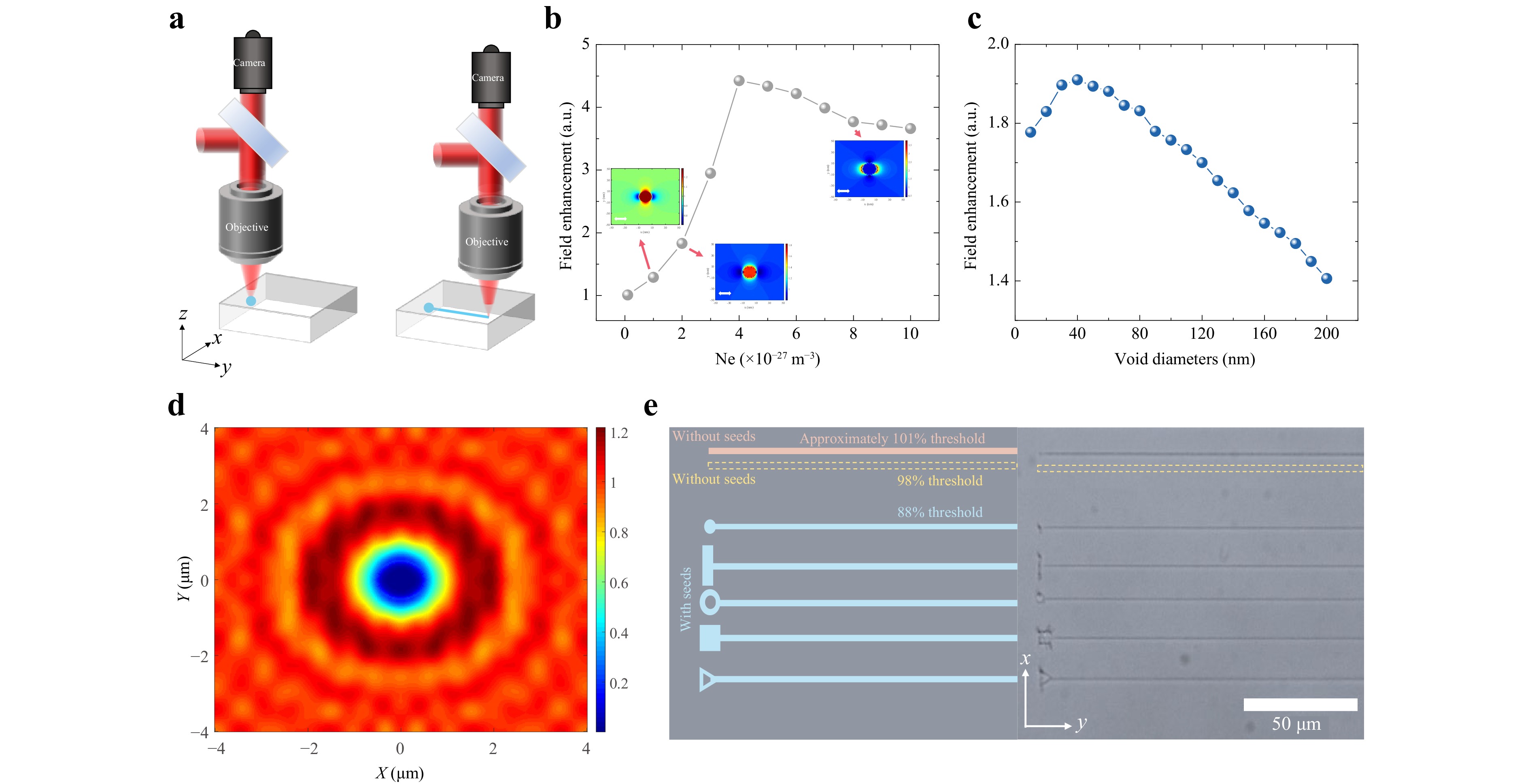
Fig. 1 Implementation scheme and theoretical analysis of femtosecond laser processing based on internal seeds. a Schematic of seed-assisted femtosecond laser processing. b Field-enhancement factor versus free-carrier concentration for a 20-nm-diameter pore. c Field-enhancement factor as a function of seed diameter at a free-carrier concentration of 2 × 1027 m−3. d Near-field enhancement for a larger seed (1 × 1 × 12 μm3) at a free-carrier concentration of 2 × 1027 m−3. e Experimental validation of seed-assisted femtosecond laser processing.
1. Use the laser power above the modification threshold (without seeds) to fabricate initial seeds inside the material.
2. Adjust the laser power below the modification threshold (without seeds) and scan outward from the modified seeds.
3. Grind and polish both ends of the sample to expose the modified lines to the surface, then chemically etch the modified lines.
Once the initial seeds are formed, their near-field enhancement modulates subsequent laser intensity, thereby increasing local energy absorption and lowering the modification threshold. During further femtosecond scanning, the newly modified regions serve as new seeds for adjacent areas, enabling sub-threshold material modification32. In situ measurements (Fig. S1) confirm that the seed structures altered optical absorption, leading to enhanced absorption and reduced transmittance.
We next performed simulations to qualitatively examine near-field enhancement. Incorporating carrier excitation and transient material response under femtosecond irradiation, we calculated the near-field enhancement factor versus free-carrier density for a 20 nm spherical seed (Fig. 1b). The results reveal that near-field enhancement initially increases and then decreases with rising carrier density. The inset displays the optical field distribution at each carrier density, with white arrows indicating polarization. Notably, as the carrier density increases, the enhancement direction shifts from perpendicular to parallel relative to the polarization. Fig. 1c shows the dependence of near-field enhancement on seed size at a fixed free-carrier density of 2 × 1027 m−3. The enhancement initially rises before declining, consistent with the trends reported by Rana Asgari Sabet et al32. To further evaluate the size effect, we also simulated near-field enhancement for a larger seed (1 × 1 × 12 μm3) at the same carrier density (Fig. 1d). Although the result shows that near-field enhancement persists near larger structures, its intensity is weaker than that of smaller ones. Overall, these findings indicate that near-field enhancement is co-regulated by the seed size and carrier density: when the seed size is appropriate and the carrier concentration exceeds a specific threshold, the light field near the structure will be significantly enhanced, thereby enabling sub-threshold processing.
Fabrication of sub-micrometer structures by femtosecond laser processing typically requires high-NA objectives for material modification, followed by wet etching. However, material modification created by high-NA objectives is usually too small to be resolved clearly under optical microscopy. To experimentally validate our approach, and given that simulations showed persistent near-field enhancement around larger seeds, we first used a low-NA (0.42) objective to study seed-assisted modification behavior. Given that the structural dimensions after wet etching show little difference from those observed directly by optical means before etching and exhibit a positive correlation, the wet etching step was omitted in low-NA objective processing experiments. Instead, we directly examined the modification results inside the material using optical microscopy. Fig. 1e presents the schematic and experimental validation of femtosecond laser processing based on the internal seeds. With seeds present, material modification occurs even at 12% below the threshold power required in the absence of seeds. Furthermore, Fig. 1e shows that sub-threshold modification arises regardless of the seed morphology, indicating that subsequent processing is largely independent of the initial seed shape, likely due to the “self-seeding”32 effect. Furthermore, the modification threshold with seeds remains constant with the variation of seed writing power and size (Fig. S8). Accordingly, to streamline experiments, all subsequent processing employed linear seeds.
The effect of processing parameters on seed-assisted fabrication using a low-NA (0.42) objective is presented in Fig. S2. With increasing scanning speed (with seeds), the modification threshold rises progressively and eventually converges with that of the threshold without seeds. The results indicate that scanning speed significantly affects the subsequent seed-assisted modification: a substantial reduction in the threshold requires a low scanning speed, corresponding to a higher number of pulses. This behavior is consistent with the incubation effect in light-matter interaction34–36. Considering both fabrication efficiency and threshold reduction, the scanning speed was set at 0.01 mm/s throughout this study. Fig. S2c and Fig. S2d further show that reducing the modification threshold leads to smaller structures. Fig. S3 demonstrates that laser polarization has a negligible effect on threshold reduction in the presence of seeds.
To investigate nanoscale structure fabrication, we performed a comparative study of laser processing with and without seeds using a high-NA oil-immersion objective (NA=1.3), as shown in Fig. 2. As laser power decreased, the cross-sectional characteristics of the structures after etching exhibited distinct behaviors depending on the presence of seeds. With seeds, the fabricated structures evolved through three distinct stages with decreasing laser power (Fig. 2a-a1), whereas without seeds, no such transitions were observed (Fig. 2b-b1). Fig. 2a-a2 presents representative cross-sections of seed-assisted structures at each stage after 40 minutes of etching.
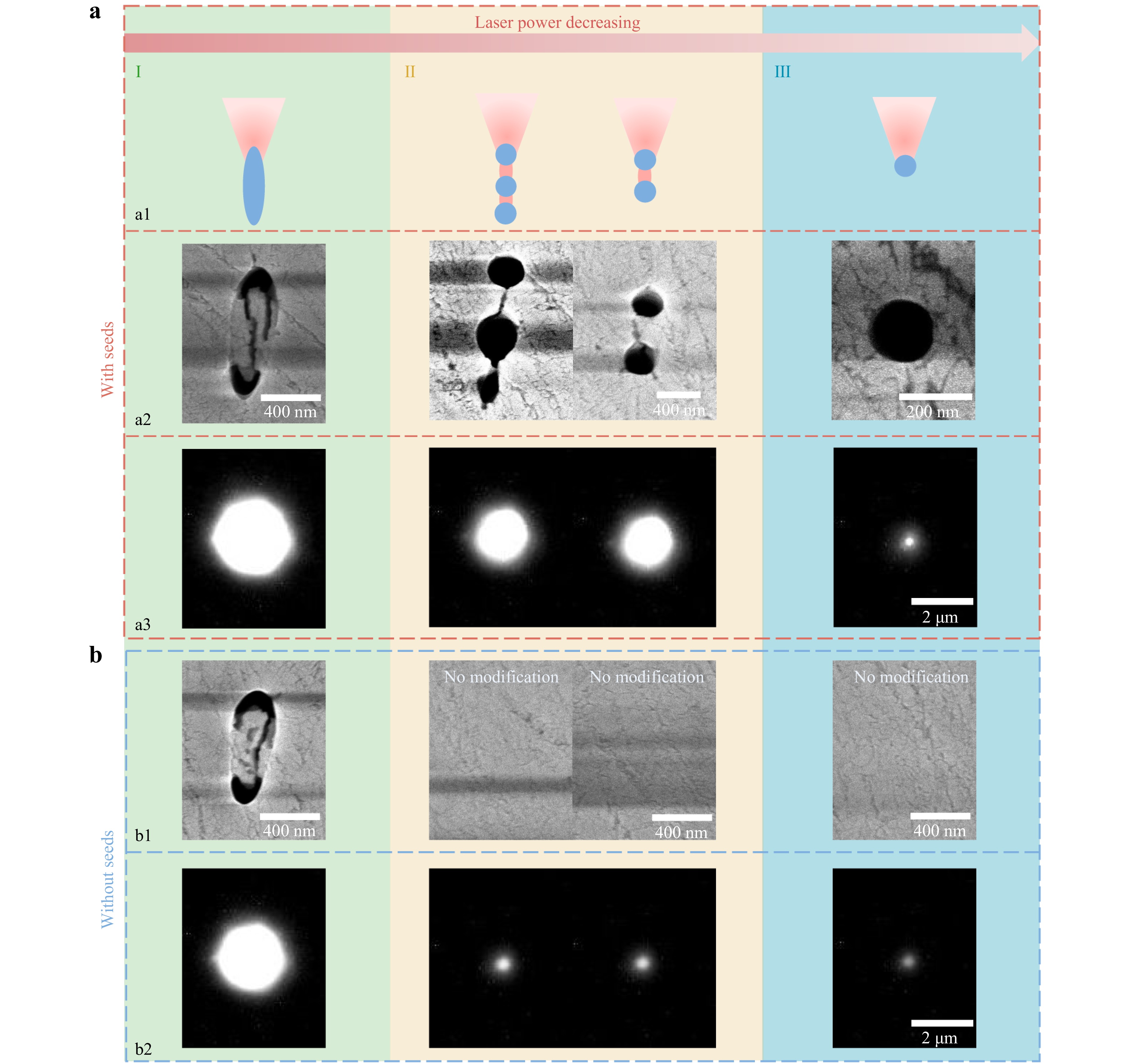
Fig. 2 Multifocal effects in femtosecond laser processing based on the internal seeds and the accompanying supercontinuum white-light spot images. a With seeds. a1 Schematic illustration of structural evolution across stages I–III versus decreasing laser power. a2 Representative SEM images after 40 min etching at each stage. a3 Representative CMOS-captured supercontinuum white-light spots at each stage as power decreases. b Without seeds. b1 SEM images after 40 min etching at each stage as power decreases. b2 CMOS-captured supercontinuum white-light spots as power decreases. SEM images in stage II share the same scale bar; all spot images share the same scale bar.
In stage I, at the highest laser power, the cross-sections of seed-assisted structures were elliptical, similar to those obtained without seeds (Fig. 2b-b1). With decreasing laser power, stage II emerges, in which the cross-sections transform from elliptical voids to multi-void structures, typically featuring two or three voids. Further reduction of laser power leads to fewer voids. The emergence of multi-void structures is associated with multifocal effects during laser filamentation37–39. At the same laser power, however, no effective material modification occurs in the absence of seeds (Fig. 2b-b1). With further reduction in laser power, the multi-voids transform into single, highly circular voids, marking stage III. At this stage, material modification remains absent without seeds (Fig. 2b-b1). These results indicate that the laser powers corresponding to stages II and III are below the modification threshold without seeds.
When a femtosecond laser is focused inside the sample, the intensity peaks are at the focal point. At low laser powers, the material undergoes only transient changes that gradually vanish, leaving no permanent modifications. As laser power increases, the system enters stage III. Without seeds, no permanent modification occurs; however, with seeds present, near-field enhancement raises the local light intensity above the modification threshold, enabling permanent modification of the material. Further increasing the laser power drives the system into stage II, which is characterized by pronounced self-focusing inside the material.
The interplay of self-focusing and plasma defocusing leads to multiple focal points forming inside the material37. Correspondingly, the cross-section in Fig. 2a-a2 clearly reveals double and triple-pore structures, corresponding to two and three foci, respectively. Importantly, the power level in this stage remains below the modification threshold without seeds, indicating that material modification can only be achieved in the presence of seeds. With further increase in laser power, the system enters stage I. At this stage, the multifocal phenomenon disappears, transforming into a single large elliptical structure. Permanent modification of the material occurs regardless of whether seeds are present.
Moreover, the ultrahigh peak power of femtosecond lasers drives strong nonlinear interactions during internal modification, producing a distinct supercontinuum white-light emission. The intensity of the white-light spot provides a direct indicator of the strength of laser-material interactions. Using CMOS imaging, we compared the supercontinuum emission with and without seeds (Fig. 2a-a3, Fig. 2b-b2). Without seeds, the white-light spot collapses abruptly from a large, bright emission to a faint, small spot once the laser power falls below the threshold, signaling the transition from effective to ineffective material modification. By contrast, with seeds the spot evolves smoothly as power decreases (Fig. S4), shrinking gradually rather than collapsing, and adopting a morphology clearly distinct from that of the seed-free case. At stage III with seeds, the white-light spot exhibits a sharply intensified central core relative to its periphery. As the laser power decreases, the central spot diminishes progressively in both size and intensity. Notably, during stages II and III, the spot characteristics differ markedly with and without seeds. These observations confirm that the intensity and spatial distribution of the white-light spot provide a practical diagnostic of whether laser-induced modification occurs. Experimentally, the onset of stage III in the seeded case is characterized by the emergence of a compact, high-intensity central spot accompanied by a fading halo in the CMOS-captured emission. At this stage, subsequent wet etching yields an isolated, nearly circular nanopore.
We next analyzed how the cross-sectional dimensions of the processed structures evolve with laser power (Fig. 3). Fig. 3a, b show the structural dimensions (a) and aspect ratios (b), respectively, after 40 min of etching for structures processed with linearly polarized femtosecond laser irradiation, both with and without seeds. As the laser power decreases, the structural width diminishes gradually, whereas the height follows a non-monotonic trajectory: it decreases slowly at first, then rises sharply, subsequently dropping rapidly, and finally decreases again at a slower rate. This behavior correlates closely with the morphology associated with the three processing stages. In stage I, the cross-section is elliptical or inverted teardrop-shaped, and its height decreases slowly with decreasing power, consistent with the trend observed without seeds. Upon further reducing the laser power, the cross-section transforms into a porous morphology. Here, we define the structure height as the vertical distance between the top edge of the topmost pore and the bottom edge of the lowest pore. Because the combined height of multiple pores exceeds that of a single elliptical cross-section, the transition from stage I to stage II produces a sudden increase in height in Fig. 3a. As the power decreases within stage II, the pore count declines; each reduction in pore number causes a substantial drop in height, yielding an overall rapid decline trend. Once only a single pore remains, the process enters stage III, wherein the height again decreases slowly with further decreases in power.
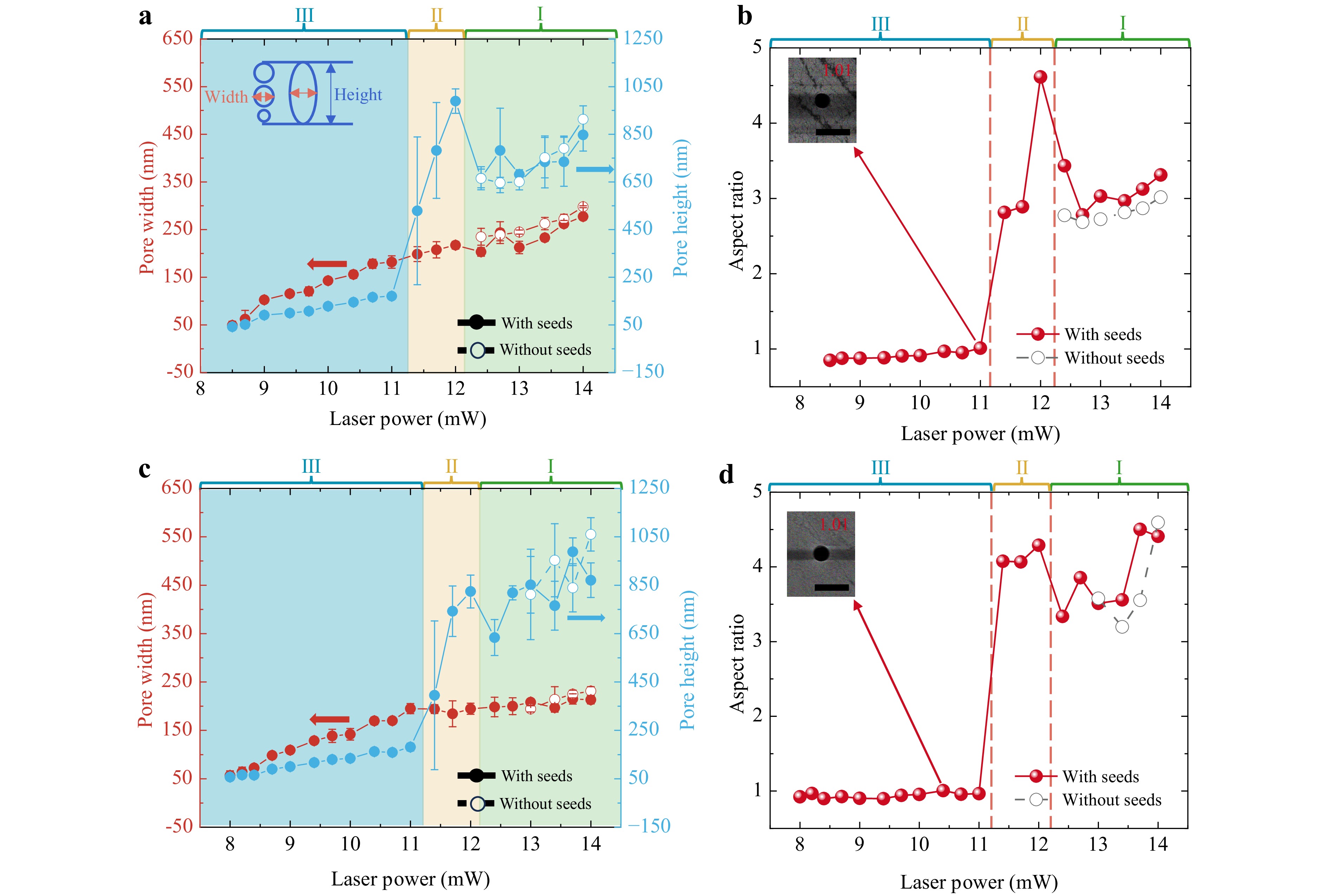
Fig. 3 Processing trends of femtosecond laser processing based on the internal seeds using a high-NA (1.3) oil-immersion objective. a, b Linearly polarized processing (polarization ⊥ scan direction): power dependence of structural dimensions (a) and aspect ratio (b) with and without seeds. c, d Circularly polarized processing: power dependence of structural dimensions (c) and aspect ratio (d) with and without seeds. The upper left of a defines the width and height definitions. Insets in b and d show SEMs of the most circular features (aspect ratio = 1.01). Inset scale bars (lower right) are 400 nm.
The aspect ratio follows a trend similar to that of the height as the laser power decreases (Fig. 3b). Specifically, the aspect ratio initially declines slowly, then rises sharply, subsequently falls rapidly toward ~1, and finally resumes a gradual decline. This behavior arises because the width decreases only gradually—far less than the pronounced changes in height—so variations in height dominate the overall aspect-ratio evolution. At 11.0 mW, we obtained a structure with an aspect ratio closest to 1 (1.01), measuring 169 × 171 nm2; the corresponding cross-sectional SEM is shown in the inset of Fig. 3b. In stage III, aspect ratios are generally < 1, spanning 0.85–1.01, with all sizes < 200 nm (Fig. 3a). Aspect ratios < 1 may result from seed-induced enhancement of local absorption aligned with the polarization, which preferentially increases the lateral width32. Fig. 3c, d show the structural dimensions (c) and aspect ratio (d), respectively, for structures fabricated with circularly polarized light, both with and without seeds, after 40 min of etching. With circular polarization (with seeds), the dimensional evolution is broadly consistent with that under linear polarization. Notably, under circular polarization in stage III the aspect ratio no longer drifts downward but remains within 0.9−1.01, while sizes are consistently below 200 nm. At 10.4 mW, the structure achieved an aspect ratio near 1 (1.01), measuring 178 × 179 nm2; its cross-sectional SEM image is shown in the inset of Fig. 3d. Collectively, these results show that the incident polarization affects the cross-sectional morphology, with circular polarization proving better suited for producing circular pore structures.
We ultimately fabricated nanopores as small as 25 × 23 nm2. To the best of our knowledge, this represents one of the smallest structural dimensions achieved to date in three-dimensional processing inside YAG crystals, marking a significant advance from the hundred-nanometer scale to the tens-of-nanometer scale. Fig. 4a displays near-circular pores fabricated by femtosecond laser processing with internal seeds after etching, spanning sizes from 25 × 23 nm2 to 202 × 218 nm2. This method not only enables the fabrication of circular pores with diameters as small as 25 nm but also allows controlled production of circular pores ranging from 25 nm to 200 nm in diameter by adjusting the laser power. Furthermore, the method has the potential to fabricate nanopatterns and other three-dimensional nanostructures within bulk materials. In principle, pores > 200 nm in diameter can be fabricated by stacking small circular pores15, highlighting both the strong processing capability and broad application potential.
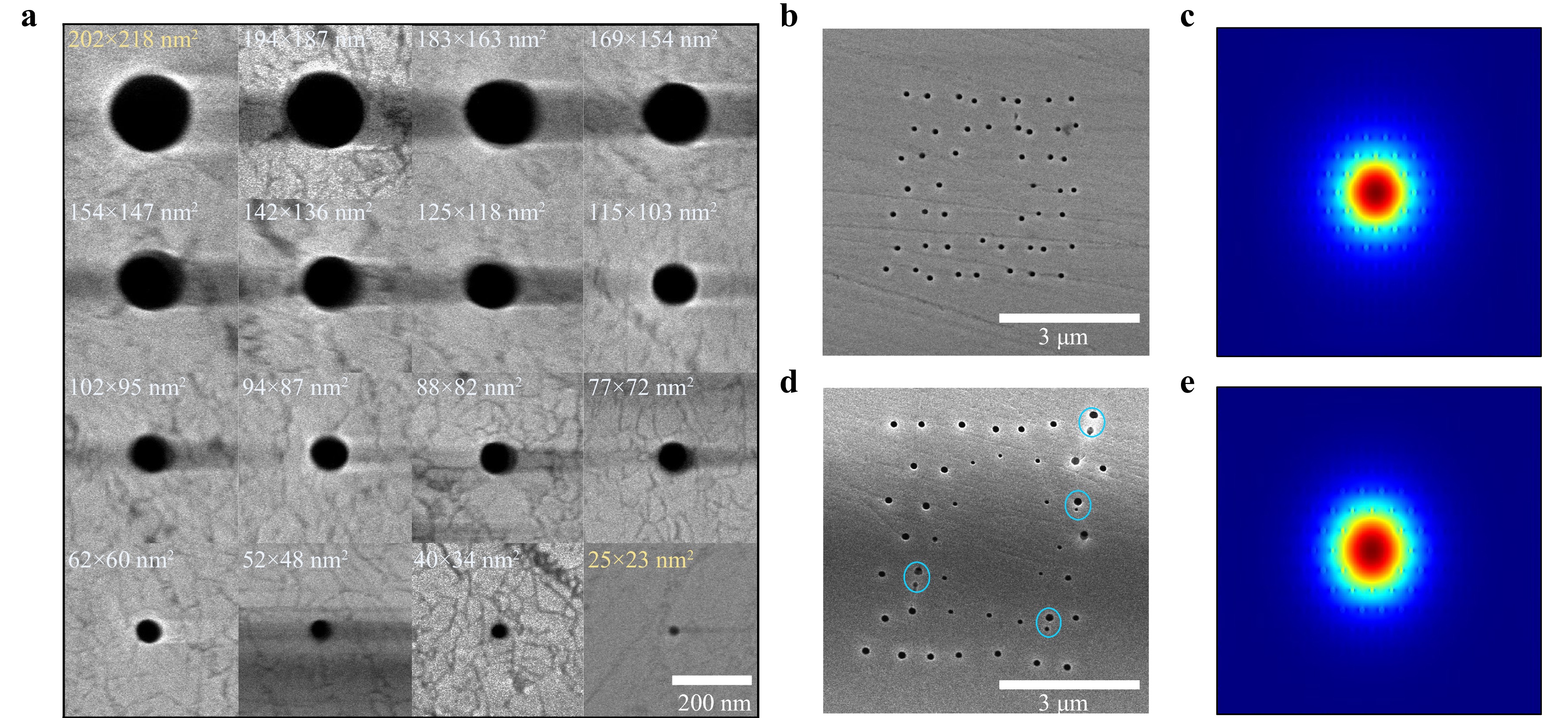
Fig. 4 Circular pores of varying size and fabrication of regular and non-uniform PhC waveguides. a Array of circular pores ordered from larger to smaller (left-to-right and top-to-bottom), with pore size annotated at each panel’s upper left; all panels share a common scale bar. b PhC waveguide fabricated with in-volume seeds, exhibiting a mean pore diameter of 120 nm. c Simulated guided mode at 1 030 nm for the PhC waveguide in b. d Non-uniform PhC waveguide fabricated with in-volume seeds; mean diameters are ~150 nm (large pores) and ~90 nm (small pores). e Simulated guided mode at 1 030 nm for the non-uniform PhC waveguide shown in d.
We fabricated PhC waveguides with a 500-nm pitch (Fig. 4b). Although slight position offsets were observed relative to the design—arising from translation-stage accuracy and environmental fluctuations—the results indicate the strong potential of the method for fabricating ultra-small, closely spaced PhC waveguides. Prior studies have shown that such structures enable effective tailoring of the dispersion properties of the materials24. We further simulated the guided modes at 1 030 nm (Fig. 4c), which confirmed fundamental-mode propagation. To showcase the programmability of structure size—drawing on low-nonlinearity PhC design principles40,41—we designed and fabricated a non-uniform PhC featuring smaller central elements surrounded by larger peripheral elements (Fig. 4d). This was achieved by controlling the processing power of the innermost structure near the minimum power required for stage III, while controlling the processing power of the outer structure near the maximum power allowed in stage III. The area marked with a circle in the image exhibits secondary focusing, which we attributed to laser power fluctuations that intermittently shifted the processing conditions between stage III and stage II. Simulation calculations confirmed its mode distribution at a wavelength of 1 030 nm (Fig. 4e), verifying that its transmission mode remains the fundamental mode. The optimization and characterization of the PhC waveguides will be performed in the future.
This method enables the successful fabrication of nanopores with dimensions down to several tens of nanometers, but certain limitations remain. With increasing etch time, the pore geometry becomes increasingly influenced by the crystal lattice orientation and gradually evolves toward a hexagonal geometry (Fig. S5). Therefore, to obtain long, straight nanopores while maintaining diameters in the tens-of-nanometer range, the etching process should be optimized—for example, by incorporating auxiliary vertical etching pores24 and reducing the etch time to suppress lattice-driven shape evolution. If such auxiliary vertical etching channels are incorporated, the feasible pore length can, in principle, be extended without limit. Nanopores approximately 100 μm long can be fabricated without auxiliary vertical etching pores. Additionally, because the geometric dimensions of the initial seeds exceed those of the ultimately fabricated structures, their presence may influence the final architecture. Several strategies can be employed to mitigate the impact of initial seeds on the overall structure, as detailed in Supplementary Note 8. Furthermore, when the size of nanopores reaches the nanometer scale, the demand for etchant may differ from that of conventional seedless structures owing to differences in chemical accessibility and modified-region morphology. The repeatability and stability of the fabricated nanopores are crucial performance metrics. We assessed these properties by fabricating nanopore arrays at different laser powers, as detailed in Supplementary Note 10. Moreover, the method can be extended to materials that exhibit high etch selectivity following femtosecond-laser-induced modification, such as sapphire. We validated the approach in sapphire and observed a lowered modification threshold (Fig. S6), confirming its broader applicability.
-
We present a method of femtosecond laser processing with wet etching based on the internal seeds that substantially lowers the modification threshold in YAG. This approach enables the fabrication of size-tunable, near-circular-cross-section nanopores spanning tens to hundreds of nanometers, with a minimum cross-section of 25 × 23 nm2. It possesses the potential to fabricate nanopatterns and other three-dimensional nanostructures within bulk materials. Our findings push 3D femtosecond-laser processing into the tens-of-nanometers regime and further reveal the structural evolution that occurs when laser power drops below the material’s intrinsic modification threshold. Using this method, we fabricate photonic crystal waveguides composed of nanopores inside YAG, as well as low-nonlinearity, non-uniform photonic crystal waveguides, validating the capability to produce complex nanopatterns and nanoscale photonic crystals inside materials. Additionally, we confirm this method’s applicability to sapphire, underscoring its broader versatility. Our work paves the way for the advancement of 3D femtosecond laser nanolithography.
-
We used a 2 × 2 × 5 mm3 YAG crystal with all faces polished to optical quality except the two 2 × 2 mm2 side faces. A femtosecond fiber laser (FemtoYL-20) delivered 1 030 nm output with 400 fs pulses at a 300 kHz repetition rate. The incident power was adjusted with a half-wave plate and a polarizing beam splitter (PBS). The sample was mounted on a motorized XYZ translation stage (Aerotech PRO165SV), enabling precise three-dimensional processing through programmed stage motion. Laser focusing was achieved with either a 50× objective (NA 0.42) or a 100× oil-immersion objective (Olympus, NA 1.3). The polarization direction was adjusted by placing a half-wave plate in front of the objective lens, while circular polarization was obtained by placing a quarter-wave plate in the beam path.
The femtosecond laser processing based on the internal seeds comprises two steps: (i) local modification with power above the material’s modification threshold, and (ii) reducing the power and initiating a line scan from the seed region at a low scan speed (Fig. 1a). After laser writing, both ends of the sample were ground and polished, followed by cleaning and immersion in 44 wt% H3PO4 for water-bath etching at 83 °C under continuous agitation by a magnetic stirrer. After etching, the sample was ultrasonically cleaned sequentially in deionized water, acetone, and ethanol. The fabricated structures were characterized by a transmitted-light optical microscope (Keyence VH-Z500) and a scanning electron microscope (SEM, SU8220).
-
This work is supported by the National Key Research and Development Program of China (2023YFB3610800).
Ultrafine three-dimensional nanostructuring in YAG via seed-enabled femtosecond-laser near-field enhancement and wet etching
- Light: Advanced Manufacturing , Article number: 38 (2026)
- Received: 17 October 2025
- Revised: 12 March 2026
- Accepted: 13 March 2026 Published online: 01 April 2026
doi: https://doi.org/10.37188/lam.2026.038
Abstract: Three-dimensional micro/nanostructures enable precise tuning of optical properties and have attracted broad interest. However, fabricating highly circular three-dimensional nanopores inside bulk materials remains challenging. Here, we overcome this barrier with a femtosecond laser–assisted wet etching strategy based on internal-seeds. Precisely induced seed defects in YAG produce localized near-field enhancement, lowering the modification threshold and, with wet etching, fabricating well-controlled, nearly circular nanopores with diameters down to 25 nm. Finally, we demonstrate programmable arrays and photonic crystal structures assembled from near-circular pores, establishing a practical route to nanoscale, in-volume three-dimensional nanolithography in crystal.
Research Summary
Nanofabrication: Seed-enabled ultrafine circular nanopores in crystal
Three-dimensional nanostructures buried inside transparent materials could enable smaller and more precise optical devices, but making tiny, highly circular pores deep inside a crystal has remained difficult. Now, Guoliang Deng and colleagues from Sichuan University report a femtosecond laser-assisted wet-etching strategy that uses internal seed defects to concentrate light locally and lower the threshold for modifying the crystal. In yttrium aluminium garnet (YAG), the method produces well-controlled, nearly circular nanopores as small as 25 nm in diameter. The team also assembled programmable pore arrays and photonic crystal structures from these features. The work provides a practical route to in-volume three-dimensional nanolithography and could support future miniaturized photonic devices.
Rights and permissions
Open Access This article is licensed under a Creative Commons Attribution 4.0 International License, which permits use, sharing, adaptation, distribution and reproduction in any medium or format, as long as you give appropriate credit to the original author(s) and the source, provide a link to the Creative Commons license, and indicate if changes were made. The images or other third party material in this article are included in the article′s Creative Commons license, unless indicated otherwise in a credit line to the material. If material is not included in the article′s Creative Commons license and your intended use is not permitted by statutory regulation or exceeds the permitted use, you will need to obtain permission directly from the copyright holder. To view a copy of this license, visit http://creativecommons.org/licenses/by/4.0/.

 DownLoad: