


-
As semiconductor manufacturing approaches its physical limits, the reliable inspection of nanoscale defects on patterned wafers has become a critical challenge, with direct implications for yield and cost1,2. The International Roadmap for Devices and Systems (IRDS) highlights that achieving efficient and high-sensitivity inspection of patterned wafers is one of the most urgent challenges in advanced semiconductor manufacturing3. Optical bright-field imaging (BFI), noted for its non-contact operation and high throughput, remains the cornerstone of patterned wafer defect inspection. However, the spatial resolution of conventional BFI is inherently constrained by the diffraction limit. Additionally, the scattering signals from deep-subwavelength defects within dense nanopatterns are weak, making them easily overwhelmed by strong background scattering and rendering them undetectable in conventional imaging inspection4–6. These inherent limitations severely compromise the sensitivity of traditional BFI. Although high-resolution electron-beam microscopy can directly resolve nanoscale defects, its low throughput, substantial operational costs, and the potential for sample damage make it unsuitable for full-wafer inspection7–10. Optical phase imaging can achieve better defect contrast, but its sensitivity to mechanical vibrations and reliance on complex reconstruction algorithms pose challenges to its practical deployment11. Several optical super-resolution methods can be used to overcome the diffraction barrier. Examples include near-field imaging12, super-oscillatory imaging13, and stimulated emission depletion microscopy14. However, their application in wafer inspection is limited by their low imaging speed and the potential for sample damage. Although capable of sub-10-nm resolution, techniques such as extreme ultraviolet (EUV) light and soft X-ray ptychography require complex high-power sources, making them prohibitively expensive for broad industrial applications6,15.
Conventional BFI is inherently passive, capturing only static and steady-state optical responses. Scattering signals cannot be actively controlled to improve the signal-to-noise ratio (SNR)15–19. This limits the development of physical tuning mechanisms for dynamic optical control. The photothermal effect achieves precisely this objective20: a high-power pump beam locally heats the nanopattern, dynamically altering its optical constants (refractive index n and extinction coefficient k)21. In silicon, which has a significant thermo-optic coefficient, an increase in temperature shifts optical resonances (e.g., Mie resonances) to longer wavelengths. This shift can induce significant changes in the scattering cross-section, producing nonlinear scattering22,23. However, applications of this effect in confocal super-resolution imaging suffer from the inherent speed limitations imposed by point scanning24,25. Although photothermal modulation has been extensively studied in tunable photonic systems, its potential for defect inspection has largely been overlooked26,27. We address this gap by harnessing the photothermal effect, enabling the active tuning of scattering for enhanced defect contrast.
In this study, we introduce photothermal modulation for defect inspection on patterned wafers and validate it through theoretical analysis and experimental results. Our method extends standard BFI by incorporating a pump-probe scheme to induce localised, controllable photothermal excitation. We developed a coupled optical–thermal model that links the pump light field, the resulting temperature rise, the probe-beam scattering field, and far-field images. This model enables accurate prediction of the pump power required to generate the desired photothermal excitation28,29. Moreover, we provide a practical method for identifying the optimal probe wavelength to maximise nonlinear scattering modulation using only the reflection spectrum of the sample. Experimentally, the strong modulation of the scattering field within the pump-excited region confirms that the process is fully reversible and non-destructive. Defects with deep-subwavelength dimensions that are undetectable at 25 °C (room temperature) become distinguishable under pump excitation, exhibiting a substantial enhancement in sensitivity and contrast. The heating and cooling processes occur within a few microseconds, enabling high-speed inspection. Consequently, our approach preserves the advantages of conventional BFI, such as high speed, wide field-of-view (FOV) within the pumped region, and non-destructiveness, while providing dynamically adjustable sensitivity. This capability enables real-time optimisation to enhance defect detectability. Beyond wafer inspection, this technique may benefit a broad range of applications, including in situ monitoring and tuning of integrated photonic devices, nanoscale sensing, and high-speed optical switching.
-
The inspection of subwavelength defects is fundamentally limited by their intrinsically weak scattering signals, which result from the complex interaction between the defect and the surrounding periodic nanopatterns2. As shown in Fig. 1, passive inspection using BFI yields low sensitivity, rendering defects, such as the left-cutting defect, unresolvable in far-field images. Previous sensitivity enhancement strategies have mainly optimised the optical configuration, such as scanning multiple wavelengths or polarisation states, to identify the conditions that maximise defect sensitivity empirically19,30. Although effective to a certain extent, these optimisations remain intrinsically constrained by the static optical response of the nanopattern. To overcome these limitations, a controllable photothermal field is introduced. Although the photothermal field is not directly observable in far-field images, it modifies the local optical constants (n, k) and consequently alters the scattering responses of both the background and the defect. As shown in Fig. 1, when a high-power pump beam generates a photothermal field around the right-cutting defect, it exhibits a pronounced perturbation in the far-field image. Furthermore, because the pump power density directly controls the local temperature increase, this method provides a dynamic and highly tunable means to enhance defect inspection sensitivity.
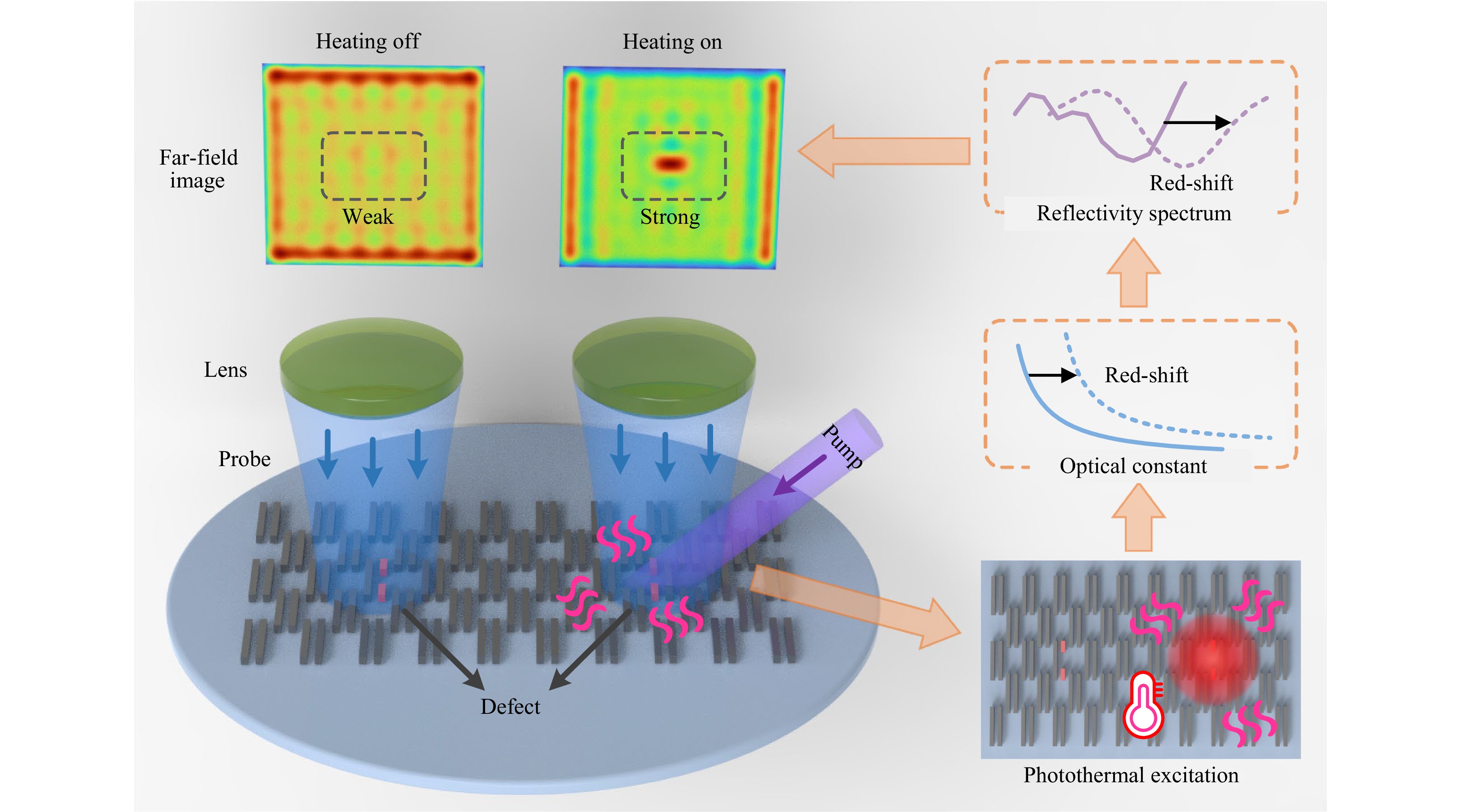
Fig. 1 Conceptual illustration of photothermal-enhanced defect inspection. A cutting defect is invisible at room temperature but becomes distinguishable when a pump-induced thermal field enhances the scattering contrast. The underlying mechanism involves beam-induced local heating, which raises the temperature of the nanopattern, altering its optical constants and red-shifting the reflectivity spectrum. The spectral shift modulates the probe scattering and enhances defect detectability.
We quantified the temperature-induced modulation of the nanopattern’s scattering using finite-difference time-domain (FDTD) simulations (Ansys Lumerical FDTD, Ansys Inc.). Temperature-dependent silicon optical constants were implemented using empirical dispersion models (Supplement S1)31,32. As shown in Fig. 2a, increasing the temperature from 25 to 500 °C shifts the dispersion of both n and k. The nanopattern consists of a periodic array of twin silicon nanowires on a silicon-on-insulator (SOI) substrate, with nanowire dimensions of 1000 nm (length) × 80 nm (width) × 75 nm (height) and a 160 nm gap, atop a 1 μm-thick buried oxide layer. Fig. 2b shows the reflection spectra at different temperatures. Spectral features at wavelengths shorter than 600 nm redshift appreciably with increasing temperature, whereas longer-wavelength features remain nearly invariant, which is consistent with the thermo-optic response of silicon in Fig. 2a. The spectra at 25, 400, and 800 °C (Fig. 2c) reveal a strong redshift of the 500 nm absorption band. By contrast, the 450 nm feature shows a weak shift despite larger changes in n and k at that wavelength. To identify the origin of this abnormal behaviour, we calculated the backward scattering cross-section, σsca-b, of the twin nanowire unit without the substrate (Supplement S2)33. The spectra of σsca-b (Figs. 2d, e) exhibit a resonance near λ = 500 nm that redshifts strongly with temperature, while no additional resonance features are present34. Because photothermal heating is confined to the silicon nanowires, only the spectral features associated with the nanopattern show spectral shifts. As shown in Fig. 2f, at λ = 488 nm, σsca-b increases to 243% of its value at 25 °C upon heating to 600 °C. By contrast, at λ = 508 nm, it plummets to just 16%. These trends highlight the strong wavelength-selective modulation of the scattering by photothermal excitation23. The highly nonlinear scattering at wavelengths on the flanks of the resonance band indicates that the probe wavelength should be selected to match the intrinsic resonance of the nanopattern to maximise defect sensitivity.
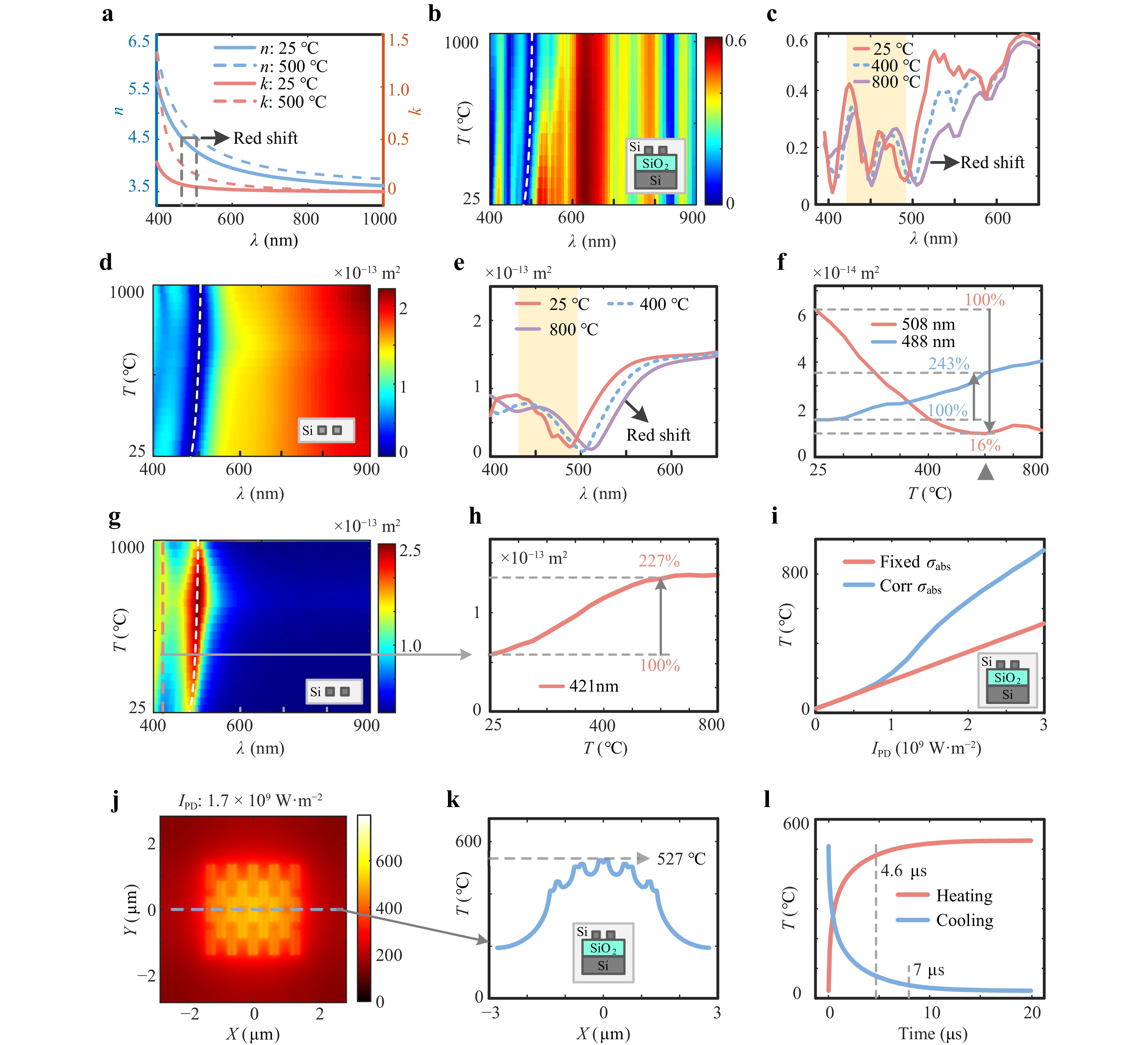
Fig. 2 Photothermal conversion and resulting scattering modulation. a Temperature-dependent n and k of silicon show an increase from 25 to 500 °C. b, c Reflection spectra of the twin-nanowire unit show a redshift with increasing temperature (length: 1000 nm, width: 80 nm, height: 75 nm, gap: 160 nm). d, e Backward scattering cross-section of the twin-nanowire unit confirms the temperature-sensitive 500 nm resonance. f Wavelength-dependent nonlinear scattering at 488 nm (short-wavelength side of resonance) and 508 nm (long-wavelength side of resonance). g Thermally-induced resonance redshift of the absorption cross-section σabs for the twin-nanowire unit. h Temperature-dependent σabs at the 421 nm pump wavelength. i Heat-transfer simulation showing the relationship between the excited thermal field and power density IPD for fixed σabs and temperature-dependent σabs. j, k Steady-state temperature distribution at IPD = 1.7 × 10⁹ W·m−2. l Transient heating and cooling dynamics with characteristic response times of 4.6 and 7 μs, respectively.
A portion of the incident energy is inevitably absorbed and converted into heat, with the fraction determined by the material properties and nanostructural topography35,36. Silicon, as an indirect-bandgap semiconductor, exhibits intrinsically weak visible-light absorption. Nevertheless, the resonance of subwavelength nanostructures can substantially enhance this absorption34. However, photothermal heating is often negligible in conventional inspection for several reasons, including a mismatch between the illumination wavelength and the structural absorption band, insufficient optical power density, and efficient heat dissipation into the surrounding medium. To evaluate the pump-induced temperature rise, we express the absorbed optical power as Pabs = IPD × σabs, where IPD is the pump illuminating power density, and σabs is the absorption cross-section. Using the same FDTD model employed for the scattering cross-section (Supplement S2), the calculated absorption cross-section shows a resonance feature around λ = 500 nm, which redshifts with increasing temperature (Fig. 2g). Because the probe wavelength is selected within this resonance band, the pump wavelength must be positioned outside to avoid spectral overlap, which interferes with the far-field image. We selected a pump wavelength of 421 nm, which is sufficiently separated from the resonance band while still providing appreciable absorption (Fig. 2h).
The thermal response was modelled using a finite-element heat transfer solver (COMSOL Multiphysics, COMSOL Inc., detailed in Supplement S3). Given the low thermal conductivity of the SiO2 layer in the SOI stack, heat tends to remain localised within the top silicon nanopattern. Assuming a constant σabs = 6.38 × 10⁻¹⁴ m2 (its room-temperature value at λ = 421 nm), the temperature rise increases linearly with IPD (red line, Fig. 2i). However, the thermally-induced resonance redshift enhances the absorption at a fixed pump wavelength, leading to a strongly nonlinear thermal response (blue curve), where the absorbed power, and thus the temperature rise, are significantly higher than the linear prediction. This highlights the need to model the temperature-dependent σabs (T) dynamically. At a pump power density of 1.7 × 10⁹ W·m−2, the simulated steady-state temperature distribution (Fig. 2j) exhibits a localised peak exceeding 527 °C (Fig. 2k). Furthermore, to assess the feasibility of high-speed inspection, we analysed the transient heating and cooling dynamics (Fig. 2l). The characteristic response time is defined as the time to reach 90% of the steady-state temperature change, which is approximately 4.6 µs and 7 µs for heating and cooling, respectively37. Both times are much shorter than typical camera integration times, confirming that the photothermal process is instantaneous for inspection. Importantly, the applicability of this mechanism is not restricted to a specific nanopattern geometry but instead relies on the presence of optical resonance modes in the background structure. Once the probe wavelength within a photothermally sensitive spectral region is selected, the photothermal scattering modulation demonstrated in this study is expected to occur. In summary, through coupled optical-thermal analysis, we elucidated the mechanism of photothermal-induced scattering modulation. Light absorption induces heating, alters optical constants, and modulates the scattering field. This analysis provides a robust method for identifying the optimal probe wavelengths and enables the prediction of the temperature rise from the applied pump power density.
-
To evaluate the effect of photothermal excitation on defect detectability, the near-field response is computed by FDTD. We propagated it to the far field using a vector diffraction imaging model that rigorously incorporated polarisation coupling (Supplement S4). For the cutting defect in the nanopattern of Fig. 2b, the simulated far-field images at 465 nm for 25 °C and 800 °C are shown in Fig. 3a. At 25 °C, the defect is essentially indistinguishable in the raw image owing to the strong background scattering from the nanopattern. Differential imaging with a defect-free reference revealed a weak residual defect signal. Defect detectability was quantified using a contrast metric defined as Cont = Idef / Ibg, where Idef is the maximal defect intensity in the differential image and Ibg is the average background intensity in the raw image2. At 25 °C, the cutting defect exhibits a low contrast of 0.08. By contrast, at 800 °C, the defect becomes directly observable in the raw image, and differential imaging yields a contrast of 0.35, approximately a fourfold enhancement, which is primarily because of the substantial increase in defect-scattering intensity. The intensity profiles extracted from the differential images further show that the defect-perturbation signal had a FWHM of 619 nm and 757 nm at 25 °C and 800 °C, respectively. Tuning the probe wavelength to 503 nm (Fig. 3b) yielded similar results. The defects were difficult to detect at 25 °C (Cont = 0.12); however, the contrast increases to 1.02 at 500 °C, indicating an enhancement of nearly an order of magnitude. For λ = 503 nm, which lies slightly longer than the absorption resonance, the redshift suppresses background scattering while enhancing defect scattering, leading to a pronounced contrast gain. Pronounced defect-contrast enhancement emerged when the excitation temperature reached ~200 °C and remained significant over a broad range up to ~600 °C, as illustrated in Supplement S5, indicating that the proposed mechanism does not require a sharply defined temperature threshold. A comparable improvement is observed for a Bx bridge defect at a probe wavelength of 457 nm (Fig. 3c), where the contrast increases from 0.15 at 25 °C to 0.38 at 800 °C, yielding substantially improved distinguishability. The enhancement is confined to a specific spectral window, as demonstrated by the negligible contrast change at the probe wavelength of 581 nm, which is far from the absorption band (Fig. 3d). Overall, these far-field imaging simulations confirmed the wavelength selectivity of photothermal contrast enhancement. In Fig. 3, the extracted FWHM values range from approximately 600–1000 nm, which is comparable to the diffraction limit of the imaging system (0.61 λ/NA ≈ 750 nm). This indicates that the defect perturbations captured by SPM2 are resolution-limited, similar to conventional BFI. Consequently, SPM2 is intended for high-sensitivity defect inspection rather than precise morphological characterization. Accurate determination of the defect shape and size relies on scanning electron microscopy (SEM) review, as is typical for deep-subwavelength structures.
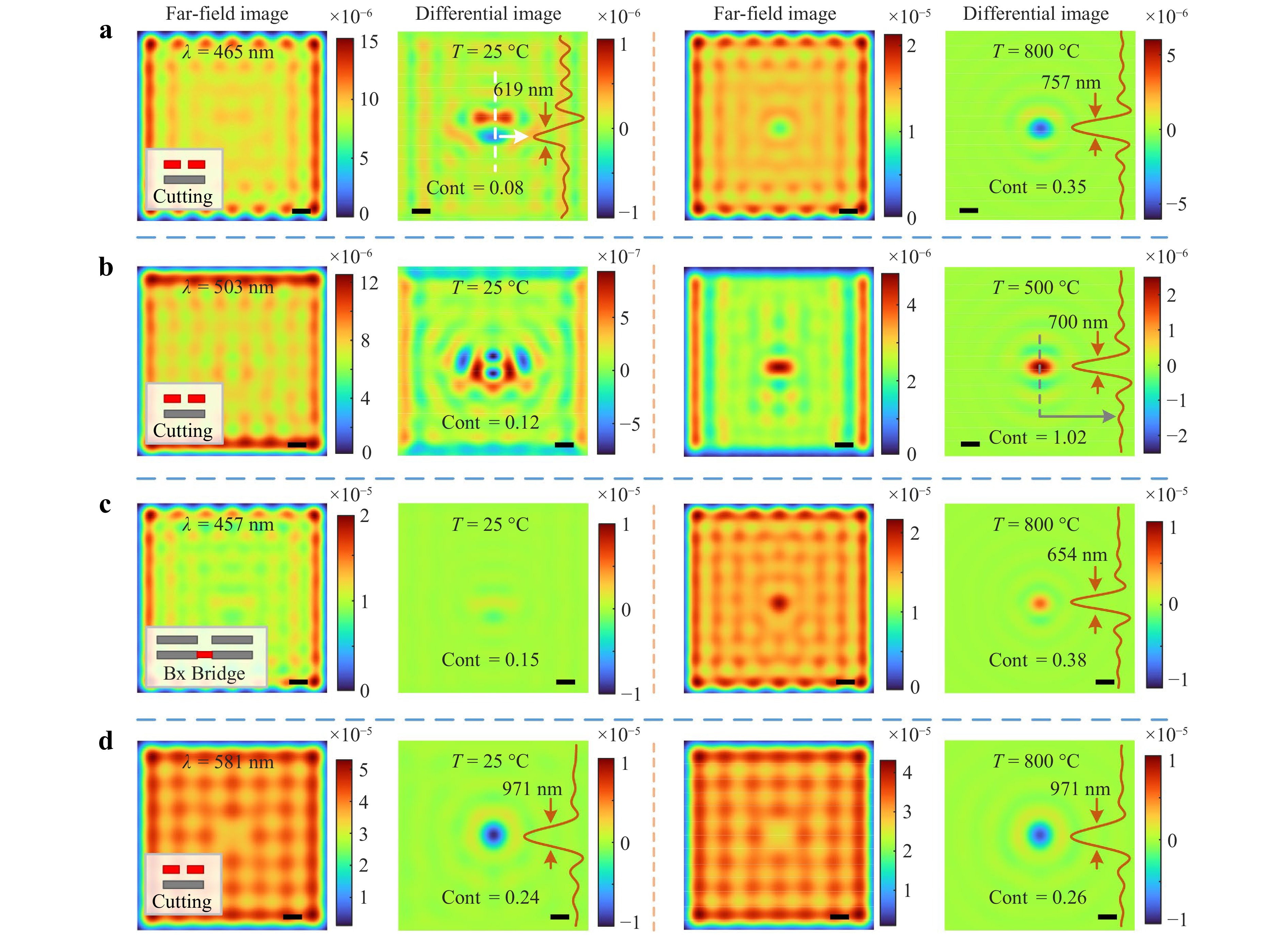
Fig. 3 Photothermal enhancement of defect inspection in far-field imaging simulations. a Far-field images and differential results for a cutting defect at 25 and 800 °C with a probe wavelength of 465 nm. The contrast is enhanced from 0.08 to 0.35. b Contrast in the far-field image is improved from 0.12 at 25 °C to 1.02 at 500 °C for the cutting defect with a 503 nm probe. c The contrast in the far-field image is enhanced from 0.15 at 25 °C to 0.38 at 800 °C for a Bx bridge with a 457 nm probe. d At 581 nm (far from the resonance band), contrast shows negligible change over the temperature range of 25–800 °C, confirming spectral selectivity. Intensity profiles from the differential images show the defect perturbation signals and their full width at half maximum (FWHM). Scale bar: 1 μm.
These light-field modulations ultimately originate from the underlying photothermal modulation of resonant scattering. The photothermal modulation mechanism demonstrated herein is not limited to SOI platforms. In general, contrast enhancement arises from temperature-induced modulation of the resonant scattering response, which can be expressed as
$$ \Delta I\propto \frac{(dn+dk)}{dT}\cdot \frac{dR}{d\lambda }\cdot \Delta T $$ (1) where (dn + dk)/dT is determined by the thermo-optic response of the material, and dR/dλ corresponds to the spectral slope of the optical resonance. Therefore, materials with large thermo-optic coefficients and nanostructures that support resonant responses can exhibit pronounced photothermal modulation effects. In this study, the SOI platform was chosen because silicon possesses a relatively large thermo-optic coefficient, and the buried SiO2 layer provides partial thermal isolation, enabling efficient resonance modulation in the top silicon nanostructures24. More broadly, similar mechanisms may be realised in other nanophotonic systems with strong thermo-optic responses, including semiconductor, metallic, or phase-change nanostructures38.
-
A schematic of the SPM2 prototype is shown in Fig. 4a. A 421 nm high-power laser was used as the pump source. The collimated pump beam was focused onto the sample using an objective lens (OL) to excite the localised thermal field. Power was adjusted using a continuously variable neutral density (CVND) filter and monitored in real-time using a power meter (PM). A broadband white-light source coupled to a spectrometer was used to measure the reflection spectra, whereas a supercontinuum laser combined with a monochromator provided wavelength-tunable monochromatic illumination for the imaging system. A complementary metal-oxide-semiconductor (CMOS) camera captures far-field images. In the probe path, a polariser (P) and a variable aperture (VA) control the polarisation and FOV. The pump and probe beams were combined using a dichroic beam splitter (DBS), and a long-pass filter (LPF) suppressed the residual pump leakage. When the pump beam is blocked, the SPM2 system operates in a mode identical to that of conventional BFI, enabling direct comparison under identical imaging conditions. A detailed description of the prototype is provided in the Methods section and Supplement S6. The thicknesses of the SOI stacks were measured using ellipsometry39. Fig. 4b shows the measured and fitted ellipsometric parameters (Ψ, Δ) at a 55° incidence angle, yielding a 74.4 nm top-silicon layer and a 1011.9 nm buried-oxide layer. IDAs were patterned on the top-silicon layer using electron-beam lithography (EBL) and transferred to the wafer via inductively coupled plasma (ICP) etching. The etch recipe provides high Si/SiO2 selectivity, and a slight over-etch ensured complete removal of the top-silicon layer down to the buried oxide. The details of the fabrication process are provided in the Methods section and Supplement S7. Fig. 4c shows the optical and SEM images of the fabricated sample. The nanopattern consisted of twin silicon nanowires approximately 957 nm long and 73 nm wide (one array from a set with varying dimensions), with intentionally introduced cutting, Bx-bridge, and By-bridge defects. The final etch depth, measured using a contact profilometer, was approximately 75 nm (Fig. 4c).
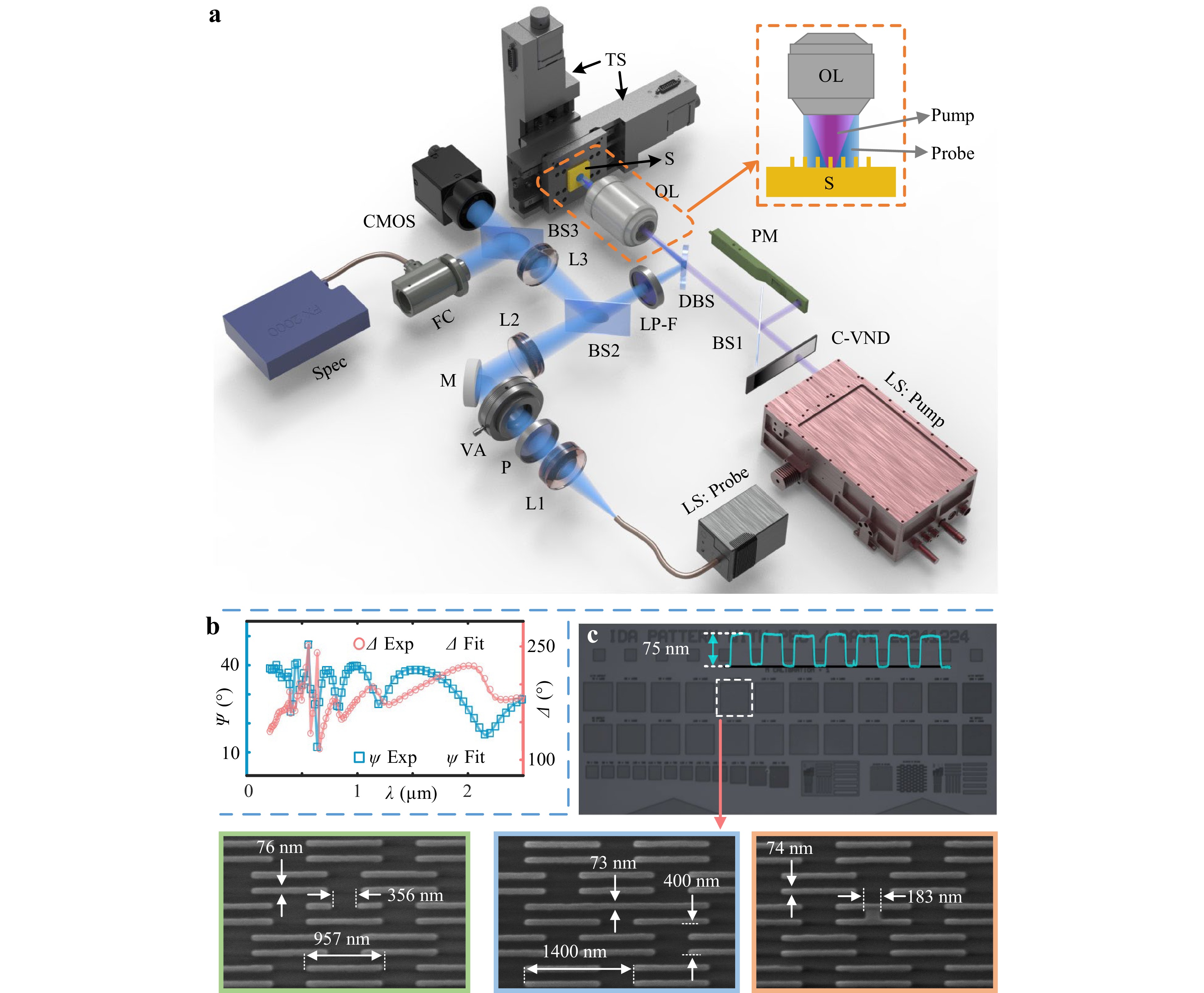
Fig. 4 Experimental setup and fabricated Intentional-defect array (IDA) nanopatterns. a Schematic of the SPM2 prototype. The prototype utilises a pump-probe architecture, featuring a 421 nm laser that emits the pump beam and a broadband source or a supercontinuum laser that generates the probe beam. b Ellipsometry-measured and fitted ellipsometric parameters (Ψ and Δ) indicate a 74.4 nm top Si layer and a 1011.9 nm buried oxide layer. c SEM images of the fabricated nanopatterns (length: 957 nm, width: 73 nm, depth: 75 nm) with cutting, Bx-bridge, and By-bridge defects, among a set of patterns with varied dimensions.
The reflection spectrum of the unpatterned SOI stack was measured using a broadband probe source (Fig. 5a). The measured spectrum agrees well with the simulated spectrum, thereby confirming the reliability of the experimental setup. The reflection spectra of the nanopatterns are shown in Fig. 4c. The VA was adjusted to ensure that the probe was filled with the nanopatterns. As shown in the right panel of Fig. 5a, the measured spectrum exhibits a distinct absorption band near 500 nm. We performed FDTD simulations using the measured geometric parameters of the nanopatterns (Fig. 4c) and accounted for the numerical aperture of the OL. The simulated reflectance spectrum showed good agreement with the experimental spectrum, including the positions of the absorption and reflection bands. A supercontinuum laser was used to examine the wavelength-dependent modulation of the scattering field under photothermal excitation. The probe wavelength was set to 510 nm on the long-wavelength slope of the resonance band, where the reflectance increases with the wavelength. Therefore, a thermally-induced redshift is expected to reduce the reflectance. The pump power was adjusted using the CVND filter until the power meter read 87 mW, corresponding to a maximum illumination power density IPD-max = 2.3 × 10⁹ W·m−2. The IPD-max evaluation method is described in detail in Supplement S8. Fig. 5b shows far-field images with the pump turned off and on, together with the intensity profile across the pump-excited region. The intensity in the pump region was strongly suppressed, reaching approximately 20% of the pump-off value. The reversibility was assessed by repeatedly exciting the same area in Fig. 5b for 25 cycles (2 s pump-on followed by 2 s pump-off) and reimaging after thermal relaxation. Differential analysis of the pre- and post-excitation optical images (Fig. 5c) shows no change in the far-field scattering, indicating that the scattering response is fully reversible under the applied photothermal excitation. To further verify the structural stability, SEM was performed after cycling. No observable changes in the nanostructure morphology were detected (Supplemental Fig. S9). The thermal model predicts a peak temperature below 800 °C, well below the melting point of silicon (1414 °C) and rapid oxidation threshold (~900 °C), supporting the non-destructive operation of SPM2 under the applied conditions40,41.
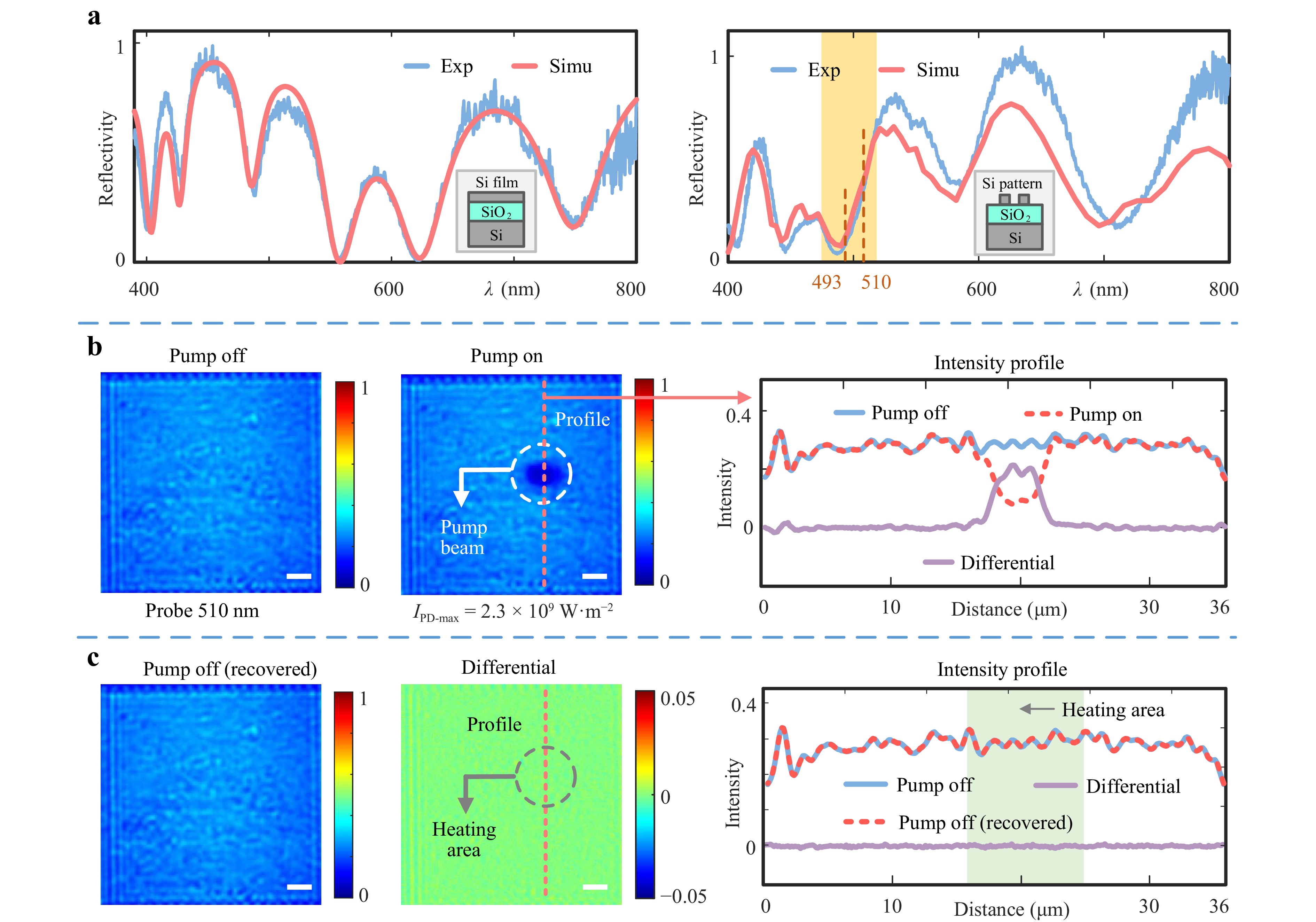
Fig. 5 Experimental observation of non-destructive scattering modulation via photothermal excitation. a Measured and simulated reflection spectra for the unpatterned SOI stack and the silicon nanopattern on SOI. b Far-field images and intensity profiles at a 510 nm probe with the pump beam in the off and on states. The pump-on state results in a significant reduction in image intensity (to 20%). c Far-field image, differential image, and intensity profile before and after repeated excitation. The lack of change in the far-field image after repeated stimulation validates that photothermal excitation is reversible and non-destructive. Scale bar: 4 µm.
Fig. 6a shows an SEM image of a cutting defect in a Si nanopattern with a width of 90 nm, along with far-field images recorded at a probe wavelength of 493 nm in the pump-on and pump-off states. Under photothermal excitation, a distinct perturbation signal appears within the pump region, whereas the pump-off image fails to reveal this defect. The intensity profiles shown in Fig. 6a highlight this change. By imaging a defect-free region of the same nanopattern, as shown in Fig. 6b, the resulting far-field images and intensity profiles exhibited only a smooth variation consistent with the near-Gaussian spatial distribution of the pump, and no defect-like features appeared. This verifies that the photothermal excitation does not generate spurious contrast and that the defect signal in Fig. 6a arises solely from the actual structural perturbation.
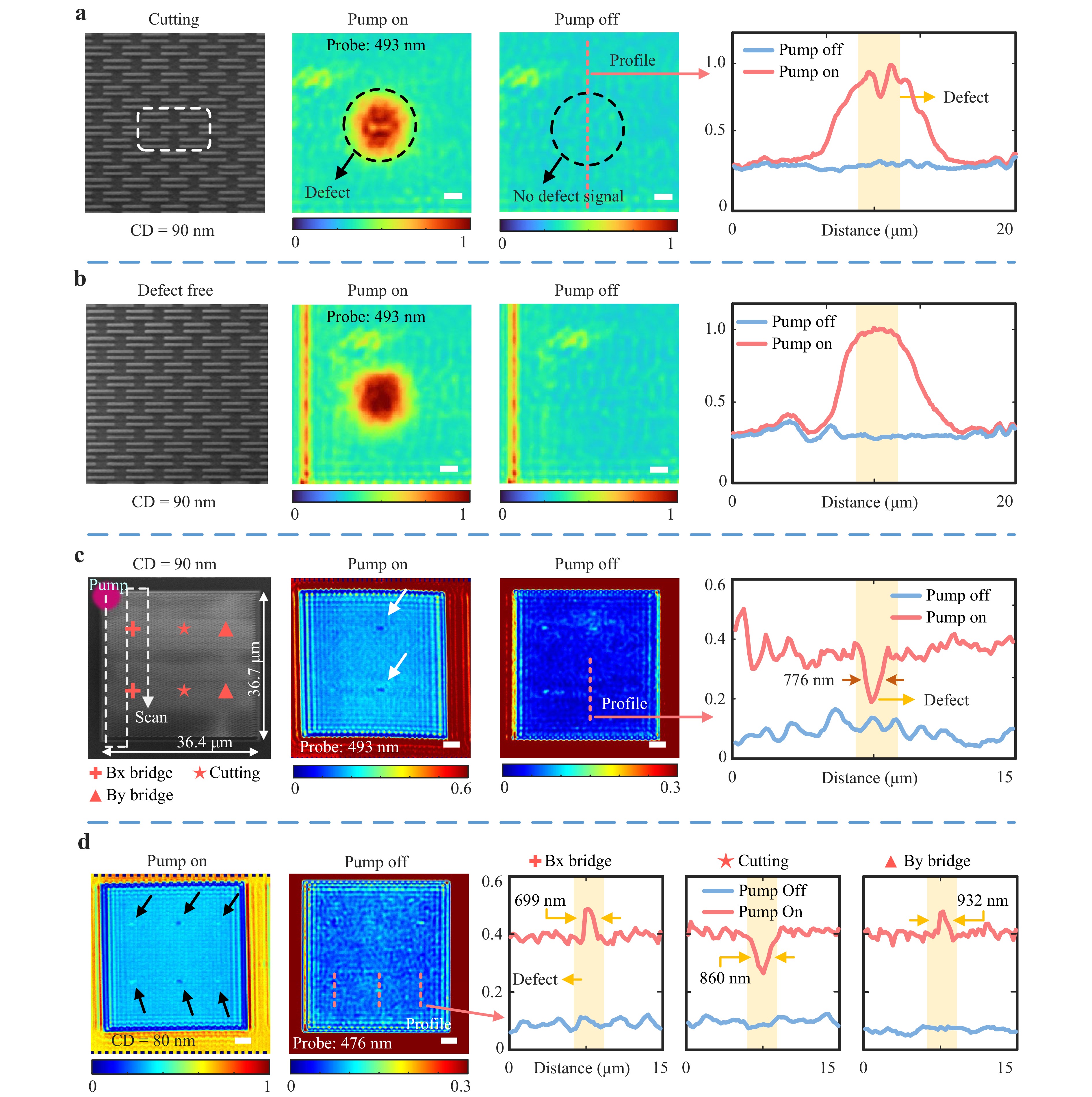
Fig. 6 Experimental demonstration of photothermal-enhanced defect inspection. a SEM image of the 90 nm silicon IDA nanopattern alongside far-field images (pump on/off) of a cutting defect. The corresponding intensity profiles demonstrate that photothermal excitation renders the previously invisible defect detectable. b Far-field image and intensity profiles of a defect-free region under pump excitation, confirming the absence of spurious signals. c Stitched far-field images acquired at a 493 nm probe wavelength; pump excitation reveals cutting defects while simultaneously attenuating the signals from Bx-bridge defects. d Stitched far-field image and representative intensity profiles for the 80 nm IDA nanopattern at a 476 nm probe wavelength. All six defects become detectable under pump excitation. The extracted FWHMs are annotated within the corresponding intensity profiles. Scale bar: 2 µm a, b and 4 µm c, d.
Under Köhler illumination, the high coherence of the pump laser produces pronounced speckle, resulting in a highly non-uniform thermal field42. Although various speckle-reduction techniques exist43, they typically incur substantial power loss that compromises photothermal excitation. Consequently, we adopted critical illumination to conserve pump power while confining thermal excitation to a micrometre-scale region. To inspect the entire nanopattern, the sample was scanned along an S-shaped trajectory using motorised translation stages, with far-field images acquired at each position. These images were subsequently stitched to reconstruct a complete far-field map under pump excitation. By matching the scan step size to the camera’s equivalent sampling resolution in the sample plane, we achieved accurate image stitching (see Supplement S10 for details). Fig. 6c shows a 36 µm nanopattern containing two cutting defects (as in Fig. 6a), two Bx-bridge defects, and two By-bridge defects. Under photothermal excitation, the two cutting defects become directly detectable at a probe wavelength of 493 nm. By contrast, the pump-off image shows no distinct perturbation, indicating insufficient sensitivity for these defects at 25 °C. Interestingly, the two Bx-bridge defects exhibited strong signals at 25 °C, which attenuated under pump excitation. Because different defects possess distinct scattering characteristics, photothermal modulation can occur in opposite directions. This suggests that inspection performance and photothermal enhancement are intrinsically linked to the defect geometry and type, which govern the scattering response and thermo-optic modulation. These results underscore the role of this method as a powerful complement to conventional BFI, significantly boosting defect detectability and reducing miss-detection rates within a fixed imaging setup. We further evaluated a nanopattern with a linewidth of 80 nm, maintaining the overall dimensions, defect count, and spatial arrangement identical to those in Fig. 6c. The stitched images, acquired using a 476 nm probe, are shown in Fig. 6d. Under photothermal excitation, all six defects (representing all defect types) become unambiguously visible. By contrast, none were detectable in the far-field image at 25 °C, where defect signals remained buried within the background noise. By leveraging the non-uniform pump beam profile, we offset the ROI from the beam centre during stitching, allowing us to compare enhancement across varying excitation strengths within a single scan (Supplement S10). These results confirm that photothermal enhancement occurs over a broad temperature range, consistent with the simulations (Supplement S5). Comparing Fig. 6c and 6d, the changes in the nanopattern linewidth lead to corresponding variations in defect dimensions, which subsequently influence the detectability of specific defect types. This comparison indicates that both defect size and background geometry are critical factors in inspection performance. Intensity profiles extracted from the three bottom defects (one of each type) are shown in Fig. 6d. Under pump excitation, all three defects generated robust perturbation signals, with the background intensity increasing from 0.1 to 0.4. Furthermore, the extracted FWHMs of these signals range from 700 to 1000 nm, which is comparable to the diffraction limit of the system and aligns with the simulations in Fig. 3. A quantitative SNR analysis further validates this improvement (Supplement S11). SPM2 enhanced the SNR of previously undetectable defects to 11.3, thereby enabling reliable inspection. Collectively, these findings confirm that the photothermal effect provides substantial, simultaneous gains in both sensitivity and contrast.
-
This work demonstrates that the photothermal modulation of nanopattern resonances provides a robust and previously overlooked mechanism for enhancing defect detectability in patterned-wafer inspection. Conventional BFI systems passively record static scattering signals44,45. By contrast, our approach introduces an actively controlled thermal field that dynamically modulates the resonant response of the nanostructures. This induces strong nonlinear variations in the scattering field, yielding substantial contrast enhancement for subwavelength defects that remain undetectable under ambient conditions. A defining feature of this method is the ability to selectively enhance or suppress defect signals by tuning the defect type and probe wavelength. Such controllability extends beyond traditional illumination-optimisation strategies, providing a novel degree of freedom in contrast engineering that is inherently absent in passive imaging. Furthermore, our approach retains the fundamental advantages of conventional BFI, including label-free and non-destructive inspection, while circumventing its intrinsic sensitivity constraints. Compared with alternative high-sensitivity strategies, such as near-field scanning, phase-retrieval imaging, super-oscillatory optics, and EUV inspection, the proposed method achieves a superior balance of sensitivity, throughput, and practical implementability1,2,46.
As an optical imaging modality, the spatial response of the inspection signal is diffraction-limited by far-field optics, whereas the imaging speed and SNR are primarily governed by probe illumination, camera acquisition rates, and the pump modulation scheme. In the current implementation, inspection throughput is constrained by the size of the thermally modulated region. Because the photothermal modulation mechanism is independent of the pump region’s dimensions, this approach is fully compatible with wide-field optical inspection architectures, requiring only the addition of a modulated pump channel. For future industrial adoption, high-coherence pump lasers can be replaced by low-coherence, high-energy sources. Such sources generate a spatially uniform thermal field across the full FOV of the probe beam, which is crucial for maximising throughput and simplifying system integration. As semiconductor nanostructures continue to shrink and their resonant modes blueshift towards the ultraviolet (UV), photothermal modulation becomes even more effective47. The stronger absorption and inherently higher spatial resolution of the UV band make it particularly advantageous for photothermal defect inspection. Notably, the underlying principle of photothermal modulation remains material-agnostic. It can be directly applied to other materials with thermo-optic responses, such as compound semiconductors or metals, significantly broadening its application potential beyond silicon-based wafer inspection48–50. For instance, III-V semiconductors such as GaAs possess thermo-optic coefficients several times larger than those of silicon, suggesting even greater modulation efficiencies. More broadly, the demonstrated photothermal modulation strategy represents a general approach for active nanophotonic control38,51. This provides a powerful method for dynamically tuning optical resonances in nanostructures, reconfigurable metasurfaces, on-chip photonic circuits, and enhanced nanoscale sensing52.
-
The experimental setup utilised a pump-probe architecture for photothermally-enhanced defect inspection. The pump source, LS-Pump, was a high-power 421 nm continuous-wave laser (FA-FHG-421-4-CW, Precilasers, Inc.). The output was collimated and attenuated using a continuously variable neutral density filter (CVND, NDL-25C-2, Thorlabs Inc.). A beam splitter (BS1, BSN10R, Thorlabs Inc.) with a nominal 9:1 transmission-to-reflection ratio directed a small fraction of the pump light towards a power meter (PM, S130C, Thorlabs Inc.) for real-time monitoring. The primary pump beam was transmitted through a 425 nm short-pass dichroic beam splitter (DBS, DM05-425SP, LBTEK Inc.) and focused onto the sample plane via an objective lens (OL, LMPLFLN20XBD, Olympus Inc.). The probe illumination was provided by two interchangeable sources (LS-Probes): a broadband white light source (EQ-99X-CAL-S, Hamamatsu Inc.) for reflection spectrum measurements and a supercontinuum laser (WL-SC-400-40, NKT Photonics Inc.) coupled with a monochromator (SR-VIS-HP20, NKT Photonics Inc.) to deliver a wavelength-tunable monochromatic probe beam for wide-field probe illumination. The probe beam emerging from the optical fibre was collimated by lens L1 (OLD2440-T2M, JCOPTIX Inc.) and passed through a linear polariser (P, FLP20-VIS, LBTEK Inc.) for polarisation control and a variable aperture (VA, SM1DP12-1A, LBTEK Inc.) to define the FOV of probe illumination. A dielectric mirror (M, BB1-E02, Thorlabs, Inc.) guided the probe beam towards L2 (OLD2466-T2M, JCOPTIX, Inc.). The probe beam was subsequently reflected by the DBS and directed through the OL to illuminate the sample, forming a wide-field probe pattern that overlapped with the pump spot. The same OL was used to collect the scattering fields. A 450 nm long-pass filter (LPF, MEFH10-450LP, LBTEK Inc.) was employed to suppress the residual pump beam. The imaging beam was directed to lens L3 (OLD2466-T2M, JCOPTIX Inc.) using BS2 (BS2, BSW10R, Thorlabs Inc.), and a CMOS camera (MER2-501-79U3M, Daheng Imaging Inc.) was used to record the far-field images. For reflection-spectrum measurements, a fibre coupler (FC, RC04FC-P01, Thorlabs Inc.) collected the imaging beam into a spectrometer (Spec, FX2000, Ideaoptics Inc.). During reference spectrum acquisition, the LPF was removed, and the DBS was replaced with a standard beam splitter (identical to BS2) to enable full-band transmission. A dielectric mirror (Type M) served as the reference sample. The two-axis lateral scanning stage (TS; M-L01.2S0, PI Inc.) featured a minimum step size of 100 nm. A photograph of the complete prototype is shown in Supplement S6.
-
The thicknesses of the SOI top-silicon layer and the buried oxygen layer were determined by spectroscopic ellipsometry (RC2-XI, J.A. Woollam). The nanostructured samples were subsequently fabricated on an SOI substrate using a standard EBL workflow. Before resist coating, the wafer surface had been treated with oxygen plasma (Diener PICO, 40 kHz, 200 W) to promote resist adhesion. A high-resolution positive-tone resist (AR-P 6200.04) was then spin-coated at 7000 rpm and soft-baked for 60 s, resulting in a resist thickness of approximately 90 nm. Pattern definition was performed using a 100 keV EBL writer (Vistec EBPG 5000plus ES). After exposure, the samples were developed in methyl isobutyl ketone (MIBK) for 70 s, rinsed with isopropanol (IPA) for 30 s, and dried on a 90 °C hotplate. The nanopattern was transferred into the top-silicon layer via ICP etching (PlasmaPro 100 Cobra) utilising an SF6/C4F8 chemistry. An etching duration of 11 s yielded a resultant etching depth of approximately 75 nm, which was verified using a contact profilometer. After etching, the remaining resist was removed using N-methyl-2-pyrrolidone (NMP). The resulting nanostructures were characterised using SEM to assess their topography. The detailed process flow is presented in Supplement S7.
-
This study was supported by the National Natural Science Foundation of China (Grant Nos. 52450158, 52175509, and 52130504), the National Key Research and Development Program of China (2023YFF1500900), the Shenzhen Fundamental Research Program (JCYJ20220818100412027), and the Guangdong-Hong Kong Technology Cooperation Funding Scheme (Category C Platform; SGDX20230116093543005). We extend our gratitude to Engineer P. Li at the Optoelectronic Micro & Nano Fabrication and Characterising Facility (Wuhan National Laboratory for Optoelectronics, Huazhong University of Science and Technology) for technical assistance during sample preparation.
Spatiotemporal photothermal modulation microscopy (SPM2) for high-sensitivity deep-subwavelength defect inspection
- Light: Advanced Manufacturing , Article number: 52 (2026)
- Received: 18 March 2026
- Revised: 01 April 2026
- Accepted: 02 April 2026 Published online: 06 May 2026
doi: https://doi.org/10.37188/lam.2026.052
Abstract: The weak scattering and overwhelming background of periodic structures fundamentally hinder the inspection of subwavelength defects embedded in dense nanopatterns. Herein, we introduce an actively tunable photothermal modulation scheme that leverages the temperature-dependent resonance shifts of silicon nanostructures to engineer their far-field scattering signatures. Localised optical heating induces a redshift in the underlying resonances, producing a strongly nonlinear change in both the defect and background scattering. This modification amplifies defect-induced perturbations and suppresses background contributions, substantially enhancing the inspection sensitivity for deep-subwavelength defects. A coupled optical-thermal model quantitatively captures the temperature rise and transient thermal evolution and predicts the resonance modulation achievable under the given pump conditions. This study establishes reversible, non-destructive photothermal resonance modulation as a general mechanism for dynamically engineering optical contrast in patterned media, offering a pathway towards high-sensitivity wafer inspection and tunable nanophotonic sensing.
Research Summary
Photothermal microscopy: Enhanced sensitivity for nanoscale defect inspection
Photothermal modulation enables label-free optical detection of nanoscale defects by dynamically tuning scattering contrast. Conventional bright-field imaging relies on static signals and often fails to resolve deep-subwavelength pattern defects. Jinsong Zhang, Jinlong Zhu, and Shiyuan Liu from Huazhong University of Science and Technology report a spatiotemporal photothermal modulation microscopy (SPM²), which uses a pump-induced thermal field to actively shift the resonant response of nanostructures. This process generates nonlinear variations in the scattering field, significantly enhancing defect visibility. The method retains the advantages of wide-field, non-destructive optical inspection while overcoming intrinsic sensitivity limits. Experiments show that defects previously obscured by noise become clearly visible, with a fivefold increase in signal-to-noise ratio. Beyond semiconductor inspection, this approach provides a general strategy for contrast engineering in nanophotonic systems, with potential applications in high-throughput inspection and active photonic modulation.
Rights and permissions
Open Access This article is licensed under a Creative Commons Attribution 4.0 International License, which permits use, sharing, adaptation, distribution and reproduction in any medium or format, as long as you give appropriate credit to the original author(s) and the source, provide a link to the Creative Commons license, and indicate if changes were made. The images or other third party material in this article are included in the article′s Creative Commons license, unless indicated otherwise in a credit line to the material. If material is not included in the article′s Creative Commons license and your intended use is not permitted by statutory regulation or exceeds the permitted use, you will need to obtain permission directly from the copyright holder. To view a copy of this license, visit http://creativecommons.org/licenses/by/4.0/.

 DownLoad: