


-
Silicon carbide (SiC) has emerged as a key structural and functional material for advanced optical systems, particularly in large-aperture space mirrors1, high-power laser optics2, and extreme-environment optical instruments3. Owing to its outstanding properties, including a high stiffness-to-weight ratio, excellent thermal stability, a low coefficient of thermal expansion, high hardness, and superior wear and corrosion resistance, SiC offers significant advantages over traditional optical materials such as glass ceramics and single-crystal silicon. These characteristics make SiC particularly attractive for applications requiring a lightweight design, high-dimensional stability, and long-term environmental robustness. Despite these advantages, the extreme hardness and low fracture toughness of SiC pose substantial challenges during precision machining processes such as grinding and polishing4,5. Mechanical material removal inevitably introduces subsurface defects (SSDs), including micro-cracks, median and lateral cracks, and fractured grain boundaries beneath the surface6–8. Such SSDs are often distributed over tens to hundreds of micrometres in depth and cannot be fully eliminated by the subsequent polishing steps without excessive material removal. If left undetected, SSDs can degrade the optical performance, reduce the mechanical strength, and compromise the long-term reliability of SiC optical components. Therefore, the accurate characterisation and control of SSDs are essential for improving the manufacturing yield and ensuring component performance.
The precise detection of defect information is a prerequisite for eliminating or suppressing SSDs. Existing SSD detection methods can be categorised into destructive and non-destructive techniques, based on whether they cause damage to the test specimen. Destructive methods involve the partial or complete destruction of the specimen to expose the defect location, followed by obtaining results through appropriate microscopic observations. Representative processing methods include chemical etching, cross-sectional microscopy9,10, and angle polishing11. These methods are simple and highly intuitive, and yield reliable experimental results. However, they are only suitable for comparative experiments. In component manufacturing inspections, both the machine and test piece must be processed from the same batch, resulting in extremely high inspection costs. To align with the manufacturing process, the inspection workflow becomes extremely cumbersome. In contrast, non-destructive testing methods utilise the differences in how internal defects within materials respond to light, sound, or electrical signals to detect anomalies and flaws within the material12,13. X-rays can undergo diffraction with crystal lattices, enabling the calculation of comprehensive stresses within a certain sample depth based on the positions of the diffraction fringes. However, the measurement results vary significantly among the different X-ray types14. Laser confocal scanning microscopy uses the confocal optical path characteristics to perform point measurements based solely on sample information within the focal plane. By moving the sample in three dimensions, this method enables the detection of scattered signals from defects at different depths within the optical components and provides depth information for SSDs15,16. Fluorescence confocal microscopy utilises the fluorescence effect of fluorescent media penetrating the SSDs in optical components under laser illumination to achieve SSD detection17–19. Kurniawan employed confocal subsurface photoluminescence spectro-microscopy to identify subsurface, electrically active screw dislocations in SiC in a non-destructive manner, achieving detection depths of up to 100 μm. However, this method is largely ineffective for detecting non-electrically active or pure edge dislocations20. The greatest advantage of this technology is its non-destructive nature, which enables the monitoring and research of SSD changes throughout the manufacturing process. However, such methods typically require high-specification experimental equipment and environments. In addition, their relatively low detection efficiency makes them unsuitable for rapid SSD inspection in large-aperture optical components. Although total internal reflection microscopy is available, its effectiveness is severely limited for non-transparent samples. Furthermore, owing to the high density of SiC, existing methods can only penetrate several nanometres or micrometres. Therefore, they are suitable only for detecting SSDs in thin SiC wafers, as they fail to observe deeper structural damage.
As a high-resolution, non-destructive, and non-invasive optical imaging technique, optical coherence tomography (OCT) has been applied extensively in the biomedical and industrial inspection fields. Its convenient and efficient testing process, coupled with its clear and intuitive imaging results, represent the prominent advantages of this technology for practical applications21–27. The high timeliness and flexibility of OCT enable it to deliver outstanding advantages in industrial in situ detection, such as three-dimensional (3D) printing in situ measurements and laser grooving monitoring28,29. Hu measured the SSDs in components using polarisation-sensitive OCT and estimated the morphology of their defects, but did not test SiC30. Israelsen constructed the first mid-infrared OCT system and applied it to real-time non-destructive testing31. At present, OCT technology faces the following challenges in industrial applications: (1) Poor environmental adaptability: Industrial vibrations and temperature fluctuations increase the image noise, compromising the detection accuracy and signal-to-noise ratio (SNR). (2) Difficulty balancing detection efficiency, resolution, and accuracy: High-resolution scanning reduces the detection efficiency, whereas device response deviations under high-frequency operation cause information loss, failing to meet production line demands for efficient and precise inspection. (3) Existing OCT technology faces limitations in inspecting samples with low surface roughness. Noise interference caused by strong surface reflections reduces or even obscures the contrast in deep-layer structure imaging. These issues constrain the widespread industrial adoption of OCT and require solutions through system design, algorithm optimisation, and hardware upgrades32.
To overcome the limitations of conventional OCT, including its strong surface scattering interference, limited spectral resolution, and high false-negative rates associated with single-mode imaging, off-axis OCT configurations have been introduced to enhance the collection of multiply-scattered photons and suppress specular reflections33,34. Building upon this concept, this study proposes an off-axis bright- and dark-field synchronous OCT (BADF-OCT) architecture for non-destructive SSD detection in SiC. The proposed system captures complementary defect information that is inaccessible to single-channel OCT by simultaneously acquiring scattered signals from two angular channels, thereby significantly improving the detection robustness. A broadband near-infrared spectral-domain OCT system operating in the 1100–1500 nm range is specifically designed to achieve both high axial resolution and large penetration depth in SiC. Combined with a dual-channel fibre array spectrometer, this system enables synchronous bright- and dark-field detection and 3D volumetric imaging. The availability of 3D data further enhances the defect recognition accuracy by enabling reliable discrimination between true SSD and surface-related artefacts. The principles of bright-/dark-field interference, data acquisition, processing, and defect identification were analysed, and the experimental results on reaction-bonded SiC samples validated the effectiveness of the proposed approach. The results demonstrate that the BADF-OCT system provides a practical and reliable non-destructive solution for SSD inspection and quality control in SiC optical component manufacturing.
-
The Fourier-domain OCT system employs low-coherence interferometry for tomographic imaging, with its optical path structure based on the Michelson interferometer. Off-axis bright- and dark-field imaging involves illuminating the sample using an off-axis light source. The photons reach the sample surface and interior, carrying the sample information as they scatter back towards the spectrometer. As opposed to traditional OCT systems, the off-axis BADF-OCT system incorporates an additional channel dedicated to the recovery of scattered photons. The mean-square heterodyne signal current at the photodetector can be expressed using the mutual interference function $ \Gamma $, as follows35:
$$ \left\langle {i}^{2}({\textit z})\right\rangle =2{\alpha }^{2}{\left| g(\tau )\right| }^{2}\times \mathrm{Re}\left[\iint {\Gamma }_{S}({\mathbf{p}}_{\mathbf{1}},{\mathbf{p}}_{\mathbf{2}},{\textit z}){\Gamma }_{R}({\mathbf{p}}_{\mathbf{1}},{\mathbf{p}}_{\mathbf{2}};{\textit z})d{\mathbf{p}}_{\mathbf{1}}d{\mathbf{p}}_{\mathbf{2}}\right] $$ (1) where $ \alpha $ is a factor that converts power into current, $ {\mathbf{p}}_{\mathbf{1}} $ and $ {\mathbf{p}}_{\mathbf{2}} $ are two-dimensional (2D) vectors transverse to the optical axis, and the subscripts $ R $ and $ S $ refer to the reference and sample arms, respectively. In addition, $ \left| g(\tau )\right| $ is the modulus of the normalised temporal coherence function of the source, which has a value of 1 when the sample and reference arm path lengths are matched, and $ {\Gamma }_{R,S}({\mathbf{p}}_{\mathbf{1}},{\mathbf{p}}_{\mathbf{2}};{\textit z})=\left\langle {U}_{R,S}({\mathbf{p}}_{\mathbf{1}};{\textit z}){U}_{R,S}{}^{*}({\mathbf{p}}_{\mathbf{2}};{\textit z})\right\rangle $. Because the incident light fields for both the reference and sample arms are Gaussian in form, the expressions are as follows:
$$ {U}_{R}(\mathbf{p},t)=\sqrt{\frac{{P}_{R}}{\pi {w}_{0}{}^{2}}}\exp \left[-\frac{{p}^{2}}{2}\left(\frac{1}{{w}_{0}{}^{2}}+\frac{ik}{f}\right)\right]\cdot \exp \left[i{\omega }_{R}t+{\varphi }_{R}(t)\right] $$ (2) $$ {U}_{Si}(\mathbf{p},t)=\sqrt{\frac{{P}_{S}}{\pi {w}_{0}{}^{2}}}\exp \left[-\frac{{p}^{2}}{2}\left(\frac{1}{{w}_{0}{}^{2}}+\frac{ik}{f}\right)\right]\cdot \exp \left[i{\omega }_{S}t\right] $$ (3) As the sample arm is incident off-axis onto the focusing lens, the expression for its light field should be multiplied by the corresponding phase delay $ {U}_{S}={U}_{Si}(\mathbf{p},t)\cdot {e}^{i\varphi (\mathbf{p},{\textit z})} $. When carrying sample information back to the spectrometer, it must pass through both bright- and dark-field recovery paths according to the following expression:
$$ \begin{split} {U}_{SDAB}(\mathbf{p};{\textit z})=\;&{U}_{Sdark}(\mathbf{p};{\textit z})+{U}_{Sbright}(\mathbf{p};{\textit z})\\ =\;&\Bigg(\int\nolimits_{{\boldsymbol{r}}_{dark\min }}^{{\boldsymbol{r}}_{dark\max }}{U}_{B}(\mathbf{r};{\textit z})G(\mathbf{r},\mathbf{p};{\textit z})d\mathbf{r}\\&+\int\nolimits_{{\mathbf{r}}_{bright\min }}^{{\boldsymbol{r}}_{bright\max }}{U}_{B}(\mathbf{r};{\textit z})G(\mathbf{r},\mathbf{p};{\textit z})d\boldsymbol{r}\Bigg)\cdot {e}^{\mathrm{i}\varphi (\mathbf{p},{\textit z})} \end{split} $$ (4) where $ {U}_{BDAB}(\mathbf{p};{\textit z}) $ is the total reflected sample field in the plane of the tissue discontinuity and $ \mathbf{r} $, $ {\mathbf{r}}_{\mathbf{1}} $, and $ {\mathbf{r}}_{\mathbf{2}} $ are 2D vectors in the plane transverse to the optical axis. $ G(\mathbf{r},\mathbf{p};{\textit z}) $ is the extended Huygens-Fresnel Greens function response at $ \mathbf{p} $ owing to a point source at $ \mathbf{r} $, which includes the effects of scattering in the intervening medium.
The bright and dark fields each have reference arms that interfere with them, and their total mean-square difference signal currents can be expressed as
$${ \begin{split} {\left\langle {i}^{2}({\textit z})\right\rangle }_{total}=\;&{\left\langle {i}^{2}({\textit z})\right\rangle }_{dark}+{\left\langle {i}^{2}({\textit z})\right\rangle }_{bright}\\ =\;&2{\alpha }_{dark}{}^{2}{\left| {g}_{dark}(\tau )\right| }^{2}\\&\times \mathrm{Re}\left[\iint {\Gamma }_{Sdark}({\mathbf{p}}_{\mathbf{1}},{\mathbf{p}}_{\mathbf{2}},{\textit z}){\Gamma }_{Rdark}({\mathbf{p}}_{\mathbf{1}},{\mathbf{p}}_{\mathbf{2}};{\textit z})d{\mathbf{p}}_{\mathbf{1}}d{\mathbf{p}}_{\mathbf{2}}\right]\\ &+2{\alpha }_{bright}{}^{2}{\left| {g}_{bright}(\tau )\right| }^{2}\\&\times \mathrm{Re}\left[\iint {\Gamma }_{Sbright}({\mathbf{p}}_{\mathbf{1}},{\mathbf{p}}_{\mathbf{2}},{\textit z}){\Gamma }_{Rbright}({\mathbf{p}}_{\mathbf{1}},{\mathbf{p}}_{\mathbf{2}};{\textit z})d{\mathbf{p}}_{\mathbf{1}}d{\mathbf{p}}_{\mathbf{2}}\right] \end{split} }$$ (5) where $ {\left\langle {i}^{2}({\textit z})\right\rangle }_{dark} $ and $ {\left\langle {i}^{2}({\textit z})\right\rangle }_{bright} $ refer to the mean-square heterodyne signal current dark and bright fields, respectively. If necessary, the optical path difference between the reference and sample arms in the bright- and dark-field modes requires an additional distance to enable simultaneous observation at different depths, and $ \left| g(\tau )\right| $ is divided into distinct values for the bright- and dark-field modes. Similarly, double cameras of the dark and bright fields have different values of $ \alpha $. The principle of the off-axis BADF-OCT detecting SSDs is illustrated in Fig. 1a.
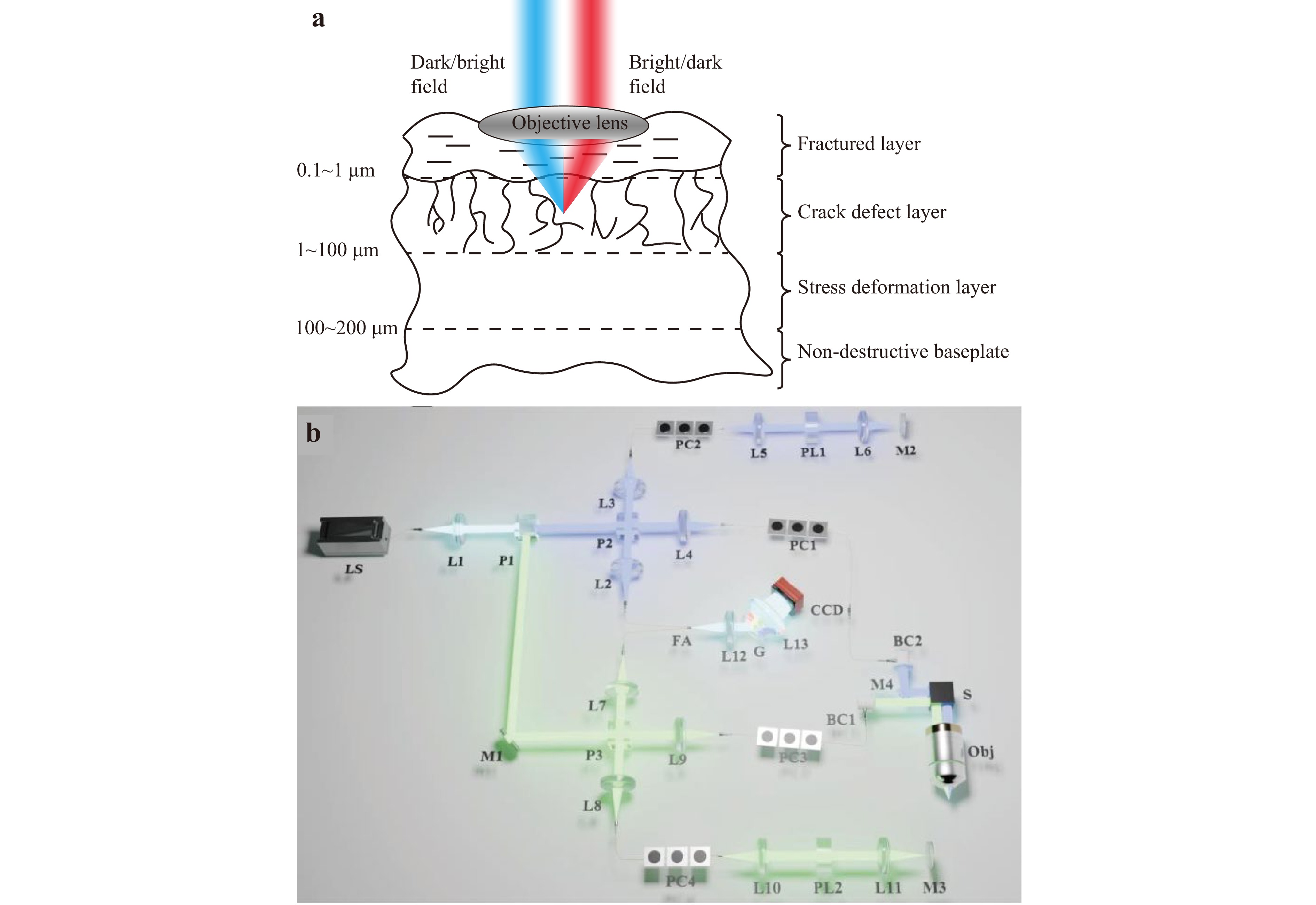
Fig. 1 a Principle of detecting SSDs in SiC using the off-axial BADF-OCT. b Schematic of the off-axis synchronous BADF-OCT system. LS: light source; L1–L13: lenses; P1–P3: beam splitters; M1–M4: mirrors; PC1–PC4: polarisation controllers; PL1–PL2: dispersion compensation elements; FA: fibre array; G: grating; CCD: camera; BC1–BC2: reflective beam collimators; S: scanner; Obj: objective lens; blue beam: composite colour light; green beam: bright field; purple beam: dark field.
-
The overall structure of the off-axis BADF-OCT is depicted in Fig. 1b. A broad-spectrum light source (SuperK FIANIUM OCT, NKT Photonics) outputs light waves that pass through the beam splitter coupling unit P1. L1 is the collimating lens. To ensure deep penetration of the SiC sample, the system employs a filtered light source with a wavelength range selected within the near-infrared band of 1.1–1.5 μm. The green beam represents the actual illumination beam and the purple beam represents the actual dark field. The illumination beam is divided by P3 into the reference arm and collected by focal lens L8, while the other part is collected by L9 into the sample arm. PC3 is used to control the beam polarisation. The beam after controlled polarisation is collimated by a reflective beam collimator that does not introduce chromatic aberrations. Using scanner S, the beam is focused using an objective lens. When reflected from the samples, the light field photons return along the original route and interfere with the reference photons at P3. Information is collected by lens L7 and sent to the spectrometer. Dark-field photons with scattered angles return along the purple beam route and interfere with the dark-field photons returning from M2 at P2. Simultaneously with the bright-field interference information, dark-field interference information is captured by the spectrometer. Owing to the special structure of the off-axis BADF-OCT system, the purple beam route can also be considered a bright field, and the green beam route can be regarded as a dark field. The spectrometer consists of a collimator, grating, and camera. The working wavelength ranges from 1.1 to 1.5 μm.
In addition, when the green beam acts as a bright field, the purple beam depicted in the figure represents the alignment-guiding beam of the dark-field optical path. Following collimation, it is intentionally injected with a radial offset from the entrance pupil centre of the telecentric scan lens, symmetrically opposite to the radial displacement of the illumination beam, so that it is focused on the sample volume, thereby establishing an additional optical signal channel. A portion of the reflected light field generated at the illuminated sample travels back along the original path of the illumination beam, forming the bright-field signal. Another portion is returned along the guided beam path, corresponding to the region outside the illumination axis and forming the dark-field signal. Although the dark-field guiding beam generates the same illumination and corresponding two-way backlight collection, by introducing a fixed optical path difference to the guiding optical path through the optical path design and combining it with the optical path adjustment function of the bright-/dark-field reference arm, a dynamically adjustable dual Michelson structure synchronous low-coherence interferometric sampling system is constructed, thereby clearly distinguishing the bright- and dark-field signals. In addition, the “coherence gate” effect resulting from the short coherence length is use to isolate the “illumination effect” of the guiding beam naturally, so that the interference signal received by the spectrometer is only the bright-field interference signal and the dark-field interference signal obtained under the single-path illumination condition.
In this system, a fibre array spectrometer is specifically designed to acquire bright/dark-field interference signals synchronously26. Employing a conventional illumination lens–grating–lens configuration, this spectrometer utilises two ports in the fibre array to transmit bright- and dark-field interference signals separately, thereby enabling the dual-channel synchronous detection of both interference signals. To provide sufficient optical path adjustment space for the bright- and dark-field signals, two 2048-pixel high-speed linear array detectors (XEN-000688, Xenics) are used to sample the 1100–1500 nm spectral band (with a 0.1 nm spectral sampling rate), achieving an axial sampling range of up to 4.2 mm. The depth corresponding to each pixel is approximately 2 μm. After resampling, the depth of each pixel is 0.54 μm. Combined with the calibration of the scanning galvanometer system, the entire system operates at a frequency of 80–100 kHz, with a sampling SNR of 92 dB.
-
We propose an optical design of a high-resolution objective lens for the off-axis BADF-OCT system to achieve SSD detection in SiC. Its operating wavelength range is 1100–1500 nm, with a centre wavelength of 1300 nm. The layout of the objective lens, which consists of nine spherical lenses, is shown in Fig. 2a. The total length of the objective lens is 81 mm. The diameter of the scanning area is 12 mm. The size of the point array in each field of view is shown in Fig. 2b, and the specific values are listed in Table 1. The black circles represent the size of the airy spot in the current field of view. The size of the light spot in almost all fields of view is close to the diffraction limit. In Fig. 2c, the transfer functions of all fields are very close to the diffraction limit. As shown in Fig. 2d, the astigmatism in the largest field of view is maintained within 20 μm, and the maximum distortion is approximately 0.02%. The longitudinal aberration is within 20 μm. Considering the working band with a 400 nm bandwidth, two double-glued lenses are included in the system to eliminate chromatic aberration. The vertical chromatic aberration is also well controlled within the range of the airy spot. The longitudinal and vertical chromatic aberrations are shown in Fig. 2e, f, respectively. The designed entrance pupil space of this objective lens is 10 mm, with a numerical aperture of 0.185. The object-side full-aperture collection angle is approximately 10.5°. For simultaneous sampling in the bright and dark fields under off-axis illumination, it can be configured to achieve an off-axis collection angle of approximately 5°.
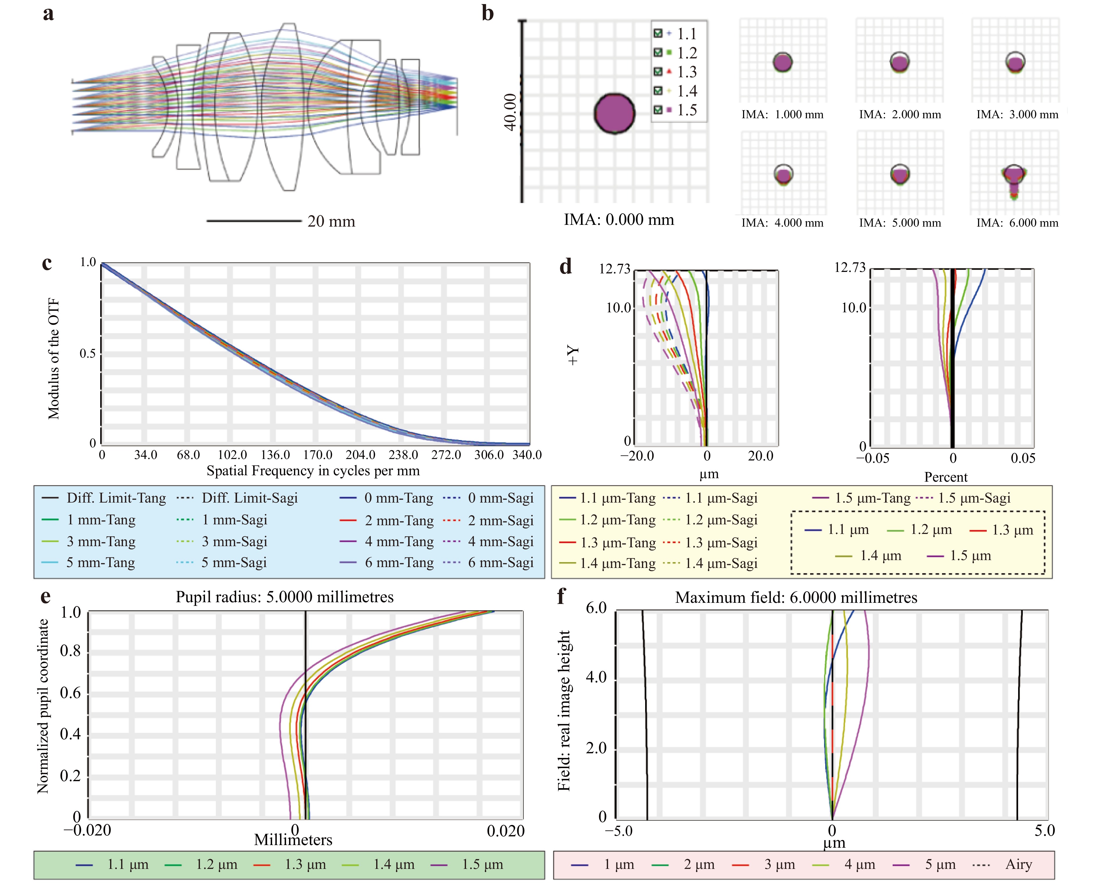
Fig. 2 Optical design parameters and performance of off-axis BADF-OCT high-resolution objective lens. a Layout of the objective lens. b Size of the spot diagrams for each field of view. 1.1–1.5: wavelength, 1.1–1.5 μm; IMA: field of view. The black circle represents the airy spot size. c Transfer functions for each field of view. Diff. limit: diffraction limit; Tang: tangential; Sagi: sagittal; d +Y: line field of view in the Y-direction. The left panel shows the field curves. The right-hand side shows the distortion. e Longitudinal aberration. f Lateral colour.
Field of view (mm) 0 1 2 3 4 5 6 RMS size (μm) 1.698 1.677 1.651 1.673 1.717 1.730 2.365 GEO size (μm) 3.271 3.963 4.432 4.713 4.792 4.452 11.371 Table 1. Spot size of line field.
-
The SSD detection process for SiC is an extension of the OCT image-acquisition method. In the off-axis BADF-OCT system, the bright- and dark-field dual channels can be synchronously imaged in the spectrometer when each has a reference arm. The basic workflow for detecting SSDs in SiC using the off-axis BADF-OCT system is illustrated in Fig. 3. During data acquisition, the sampling range and number of sampling points are first determined to generate the step voltage signal waveform that controls the deflection of the 2D galvo mirrors. Within the synchronised timing sequence of the signal generator card, the 2D mirror is steered to scan the beam along the intended path. During the dwell period at each sampling point, the spectral detector is triggered to expose and capture the interferometric spectrum. Real-time imaging preview via the control software allows for monitoring of the bright- and dark-field image acquisition. Adjusting the optical path difference between the bright- and dark-field modes ensures clear, non-overlapping tomographic images. Subsequently, the data storage function is activated to record the bright- and dark-field-synchronised interferometric spectral data from each sampling point sequentially in a dataset file. Data processing runs concurrently with the acquisition. First, the interferometric spectrum dataset is segmented into sequential single-frame spectra based on temporal tags. Spectral shaping is performed after denoising. The series of interferometric spectra then undergoes Fourier transform processing, with the results stored as a Fourier transform dataset. The Fourier-transformed interferometric spectral data are further converted into greyscale information. Based on the pre-defined 2D sampling point count and path established during data acquisition, the corresponding data from the greyscale information dataset are extracted to reconstruct a 3D greyscale image. By combining this with the preset 2D scanning sampling range information, the spatial location, size, and morphological characteristics of the SSD are extracted from the 3D greyscale image, completing the SSD detection process. Owing to the processing flow of this algorithm and the characteristics of objects that cause detection interference, such as dust and water marks on optical elements, which occupy a small surface area and emit weakly scattered return light, the signals are significantly weaker than those of smoother surfaces. Meanwhile, the light signals penetrating beneath the surface are amplified, thereby enhancing the SNR for SSDs. This method of suppressing chaotic surface signals while amplifying subsurface signals enables the morphology of SSDs to be distinguished from the interference caused by surface dust.
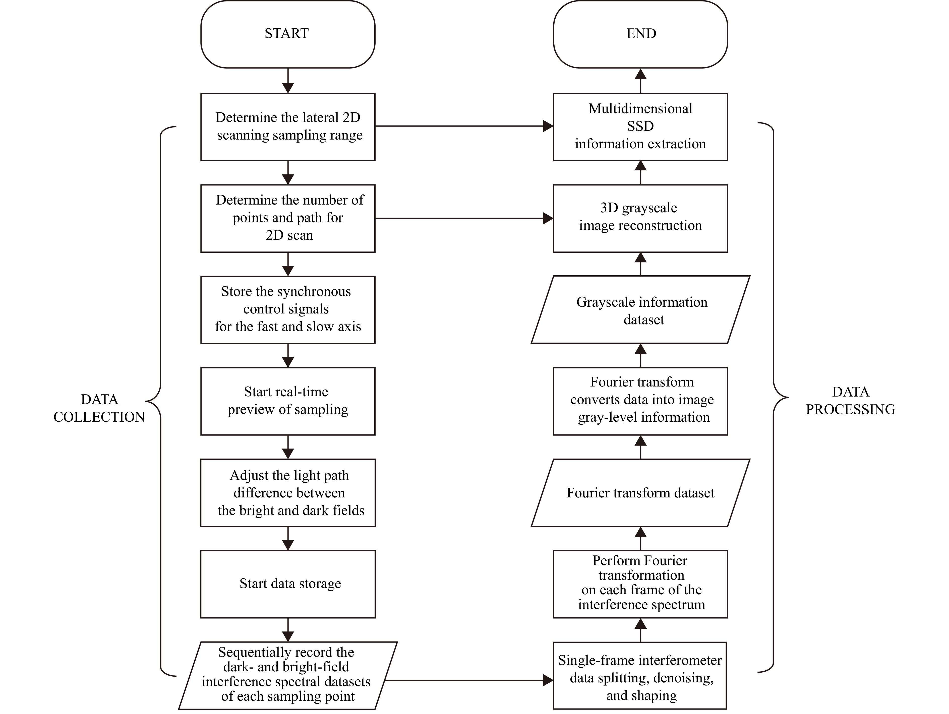
Fig. 3 Data collection and processing flow. The data acquisition component enables the simultaneous collection of bright- and dark-field signals, with synchronised preview and separate storage. During data processing, subsurface signals are amplified, whereas weak surface stray signals are attenuated, allowing for the reconstruction of 3D structural data for SSDs.
-
After completing the experimental system setup, we measured the lateral resolution, depth of focus, axial resolution, and imaging depth of the system for the experimental samples. This process validated the advantages of the dark-field synchronous scheme in terms of the SNR and detection of low-reflectance or weakly scattering targets. Fig. 4a shows a photograph of the constructed off-axis BADF-OCT system. Fig. 4b shows the positions of the scanner, objective lens, and sample.
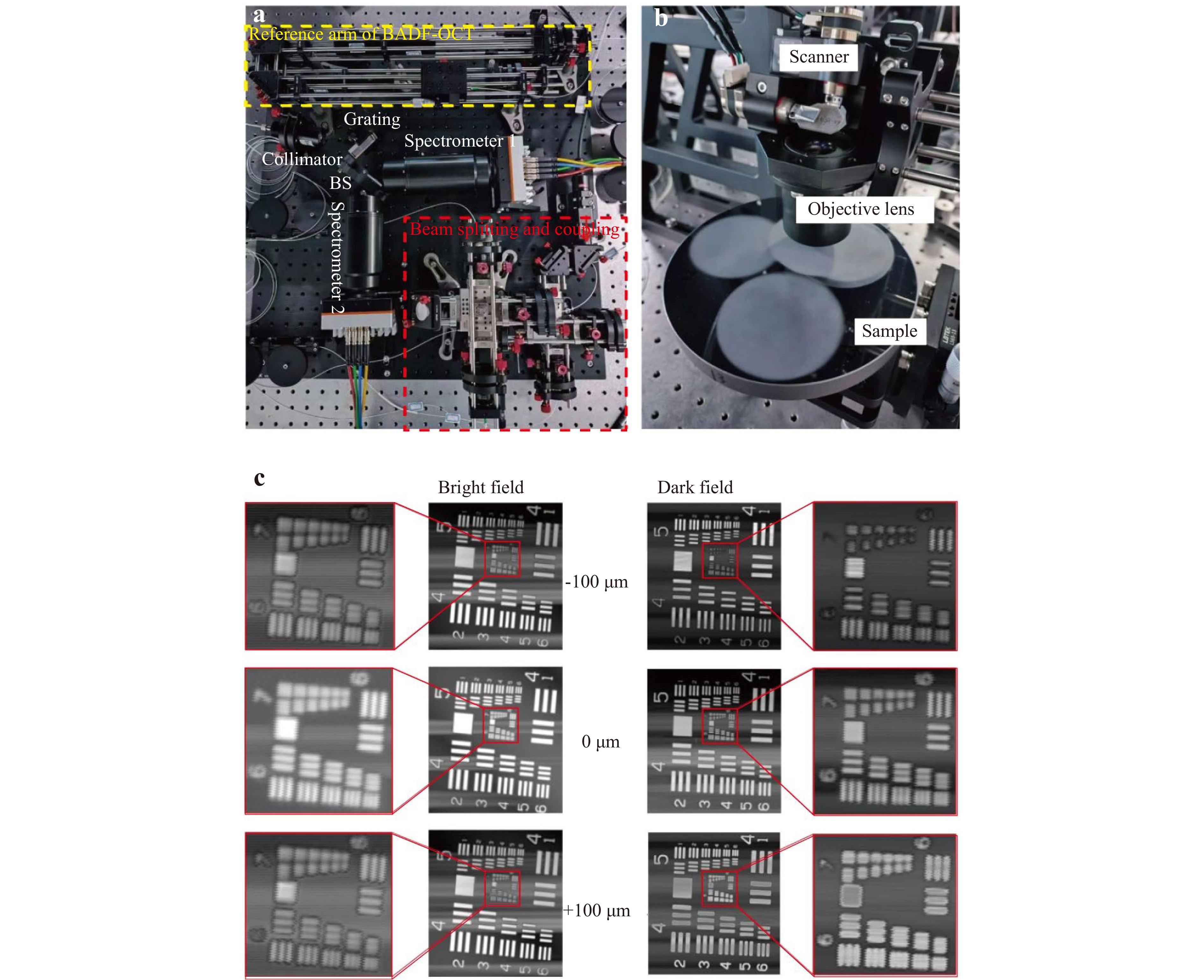
Fig. 4 a Images of the off-axis BADF-OCT system. BS: beam splitter. b Structure of scanner, objective lens, and samples. c Scanning imaging and regions of interest (ROIs) of USAF 1951 resolution board at -100, 0, and 100 μm.
Because the bright and dark fields share the same microscope objective, the light beams for their dual-path illumination occupy only half of the entrance pupil. Therefore, the lateral resolutions and detection depths of these two methods vary. Thus, we imaged the resolution plate and divided it into two parts, namely the bright and dark fields, to test their lateral resolutions separately and obtain the actual spatial resolution. Fig. 4c shows the lateral resolution and depth of the field test results for the bright- and dark-field imaging. The bright- and dark-field imaging results were extracted by directly scanning the USAF 1951 resolution test chart. The images revealed the ability to resolve the 80.6l p/mm pattern in the 6th group, 3rd row, indicating a lateral resolution of 12.4 μm for the scanning field lens in air, which was close to the theoretical calculation. Simultaneously, comparing the imaging effects at ±100 μm defocus positions from the resolution chart demonstrated that the scanning field lens depth of field met the theoretical expectations.
To ensure lateral resolution and a large imaging depth simultaneously, we constructed a spectrometer suitable for wavelengths ranging from 1.1 to 1.5 μm. A roll-off experiment was conducted to verify the axial resolution of the system. Fig. 5 shows the axial resolution test results for the off-axis BADF-OCT system. A sample arm return beam was generated by placing a mirror on the focal plane of the scanning field lens of the sample arm. Four interference spectra corresponding to the different optical path differences were obtained by progressively increasing the displacement of the reference arm. Following the Fourier transformation, four point spread functions (PSFs) were obtained, representing imaging depths ranging from shallow to deep. The results show that the average full width at half maximum (FWHM) of the diffusion function across four positions from shallow to deep was 2.935 μm, closely approximating the theoretical calculation. The sequential increase in the FWHM from the shallow to deep points resulted from the combined effects of incomplete dispersion compensation and the sampling response of the spectrometer.
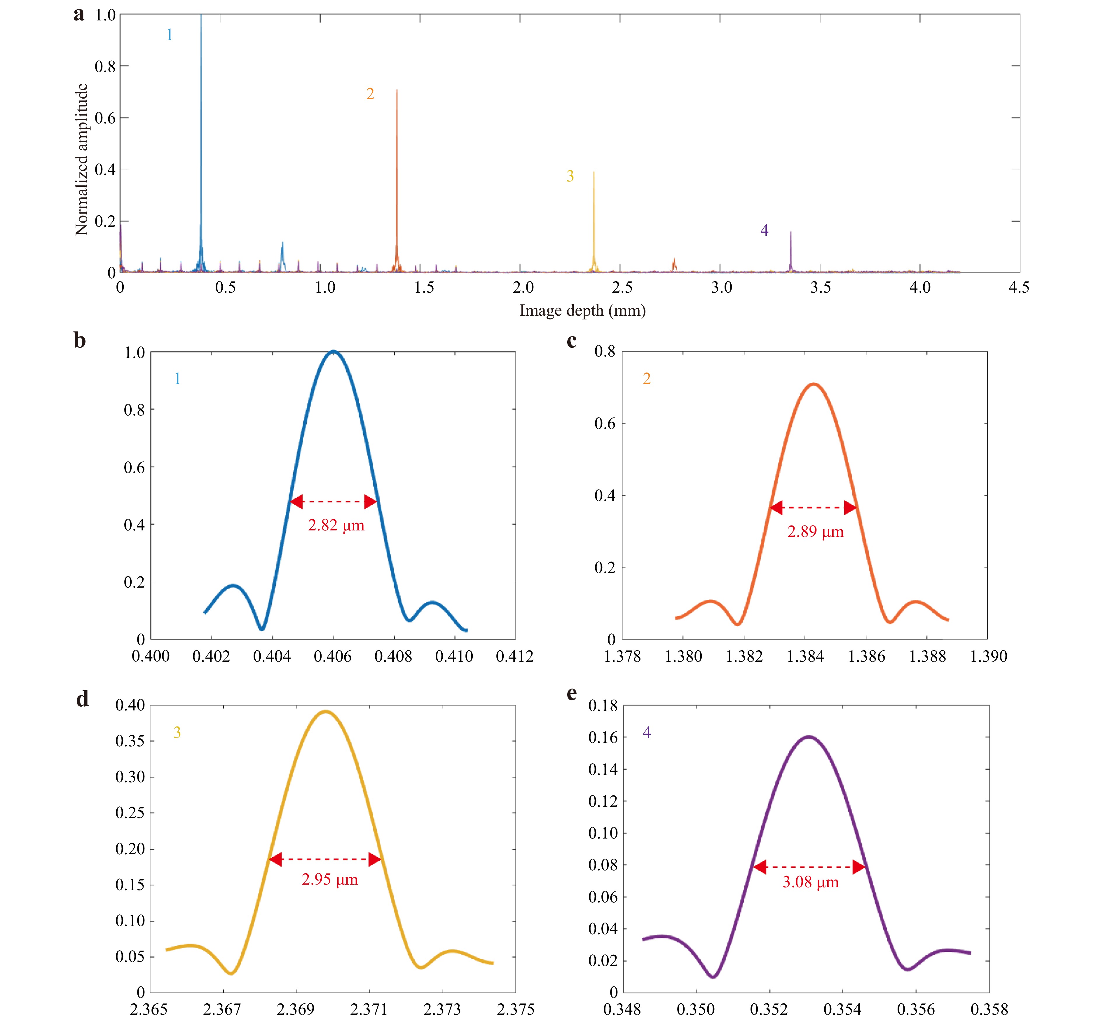
Fig. 5 a Axial PSF at different depths within the measurement range of the off-axis BADF-OCT system. b Relative peak height at the topmost point of the image, with an FWHM of 2.82 μm. The relative amplitude was 1. c 1/3 of image depth, with an FWHM of 2.89 μm. The relative amplitude was 0.72. d 2/3 of image depth, with an FWHM of 2.95 μm. The relative amplitude was 0.39. e Bottom of image depth, with an FWHM of 3.08 μm. The relative amplitude was 0.162.
Based on the measured performance of the axial resolution, lateral resolution, and depth of focus in air, the system can achieve chromatographic imaging with an axial resolution better than 1.5 μm and a lateral resolution better than 5 μm within a depth range of approximately 30 μm for SiC sample analysis. In addition, the constructed system effectively enhances the resistance to stray light interference by employing off-axis illumination, a broad-spectrum light source, and a fibre array spectrometer solution. Specifically, the off-axis illumination suppresses strong specular reflection interference from the sample surface; the near-infrared broad operating spectrum ensures a high coherent contrast even in environments with intense stray light, demonstrating exceptional environmental adaptability; and the fibre array spectrometer achieves effective spatial filtering by emitting light waves through the fibre end face. The system achieved a measured SNR of 92 dB while maintaining strong resistance to stray light interference, demonstrating robust weak signal detection capabilities. This renders it highly suitable for SSD detection in highly scattering materials.
-
The test specimens were fabricated from reaction-sintered SiC (RB-SiC), which is a two-phase composite ceramic material formed by infiltrating liquid silicon into SiC (primarily 6H-SiC) and carbon powder, followed by sintering. Fig. 6a shows a photograph of the experimental specimen. To ensure that the surface roughness and SSD of the RB-SiC specimen in the experimental testing were entirely generated by the grinding process, the surface was first polished using a cerium oxide polishing solution (with a polishing particle size of approximately 1.5 μm) to achieve a surface roughness of Sa ≈ 15 nm. At this stage, the SSDs were considered negligible and unlikely to influence subsequent SSD generation during grinding. All three regions (P1, P2, and P3) of the test specimen were ground using an RB-SiC grinding disc matching the specimen material, combined with a diamond micro-powder abrasive at 300 rpm. By setting different grinding pressures (P1: 2 psi, P2: 1 psi, and P3: 0.5 psi), progressively reduced roughness was obtained across the three regions (P1: Ra = 700 nm, P2: Ra = 630 nm, and P3: Ra = 590 nm). The surface morphology of the polished RB-SiC captured by the confocal microscope is shown in Fig. 6b, where the dark particles represent the SiC phase and the light substrate constitutes the Si phase. The SiC particles predominantly ranged between 2–10 and 20–40 μm. The Si phase acted as a “binder” between the SiC particles. The interface between the Si and SiC phases is a relatively weak area that may fracture during grinding, causing the SiC particles to detach. The detachment of large SiC particles results in a rougher surface than that of materials such as fused quartz or single-crystal silicon following grinding.
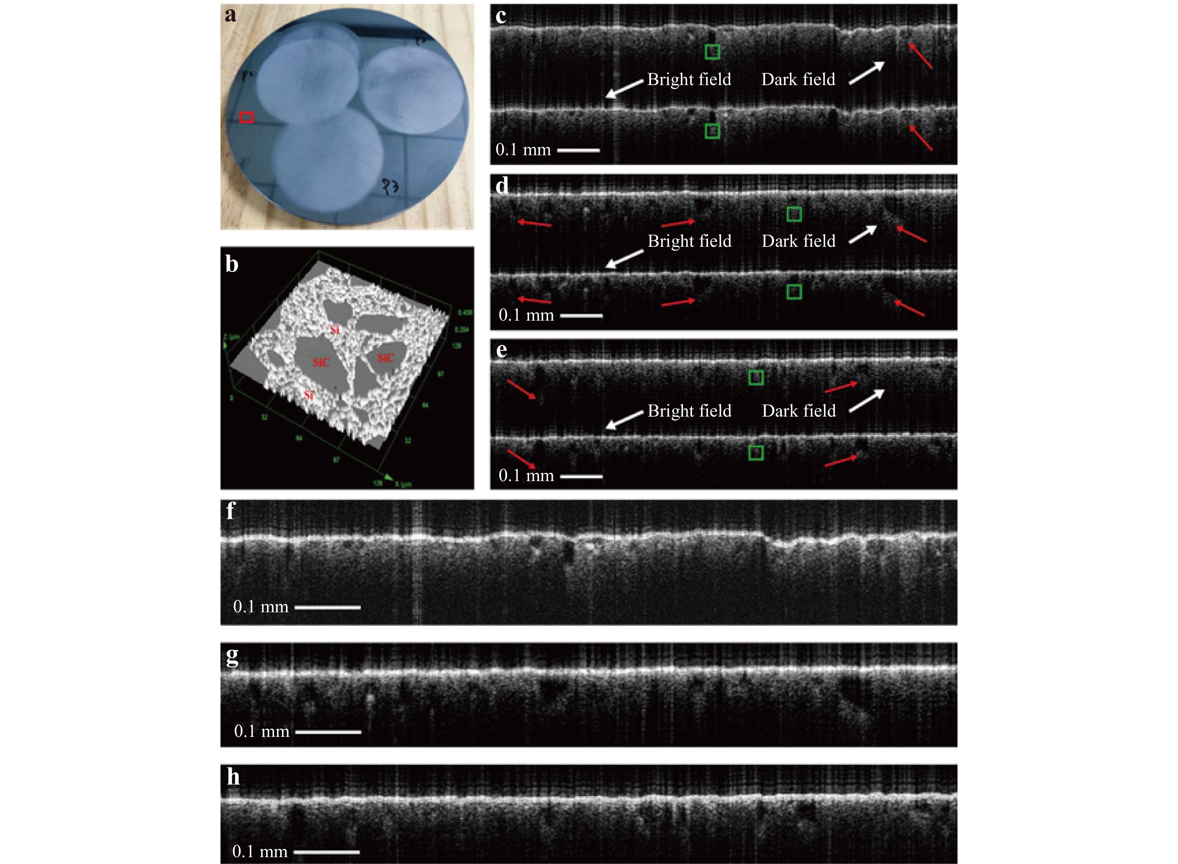
Fig. 6 a RB-SiC grinding experimental samples. The red square represents the ROI. b Image of ROI. c, d, and e show the synchronised bright- and dark-field tomographic images of P1, P2, and P3, respectively. The green box indicates the ROI used to calculate the CNR. The red arrows represent the differences between the bright and dark fields. f P1 image after merging the bright and dark fields. g P2 image after merging the bright and dark fields. h P3 image after merging the bright and dark fields.
The tomographic penetration effects measured in regions P1, P2, and P3 using the off-axis BADF-OCT system are shown in Fig. 6c-e. As indicated by the red arrow, the dark fields provided deeper information and exhibited better uniformity in the image intensity at greater depths. Notably, the smoother the surface, the brighter the surface in the picture. That is, the rougher the surface, the smaller the difference in signal strength between the surface and depth of the image. The contrast-to-noise ratio (CNR) of the dark-field ROI in P1 was 1.07, whereas that of the bright-field ROI was 1.01. In P2, the CNR of the dark-field ROI was 0.7 and that of the bright-field ROI was 0.44. In P3, the CNR of the dark-field ROI was 0.85,and that of the bright-field ROI was 0.61. In addition, the imaging results demonstrate that for RB-SiC materials, OCT tomographic images can reveal the distribution state of the SiC and Si phases within the material (large grey areas in the tomographic greyscale images represent the Si phase, whereas black shadows indicate the SiC phase). Under near-infrared light in the 1100–1500 nm spectral range, the average imaging depth for the dark-field mode (115 μm) was greater than that for the bright-field mode (102 μm). In addition, as shown in Fig. 6f-h, after merging the bright- and dark-field images, the morphology of the SiC was averaged in the bright- and dark-field images, avoiding the strong light interference of the bright field and noise of the dark field. Moreover, the advantages of dark-field imaging, that is, greater depth and superior image contrast, were effectively preserved. These preliminary experimental results between the confocal microscope and off-axis BADF-OCT system provide valid proof for SSD detection in RB-SiC.
-
Based on the results presented in Section 3.2, we conducted experiments on the SSD of RB-SiC. The fundamental morphological features of SSDs extend from near-surface locations to depths of several hundred micrometres. Although SiC particles are also present in this region and may be confused with scratches and SSDs, the surface-layer SiC exhibits a smooth surface and high reflectivity after polishing. If surface cracks exist, fractures will appear on the surface. In particular, in OCT systems, although the surface signal is angle dependent, the surface intensity in the B-scan image remains relatively uniform following angle adjustment. Fig. 7a1, a2, b1, b2 show dark-field tomography images of two locations with significant SSDs in region P1 of the sample. The imaging results demonstrate that the greyscale image obtained by directly mapping the sampled information from the OCT system exhibited high contrast. It clearly revealed the rough surface of the ground RB-SiC material and subsurface structural information within a certain depth range. Building on this, applying pseudo-colouring processing with reference to the image greyscale values will enable more accurate identification of surface interface locations and provide a more pronounced representation of the defect morphology. In addition to revealing SSD information through axial tomographic images, SSD details can also be visualised by extracting lateral cross-sectional views of different regions from the 3D greyscale data of the inspection results.
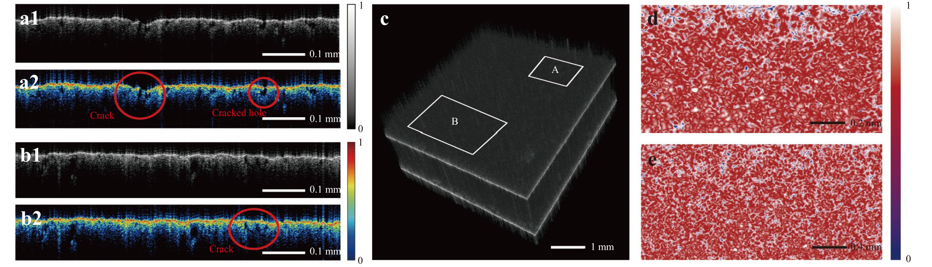
Fig. 7 Tomographic image of the measured SSD position in the P1 region. a1, b1 Greyscale. a2, b2 Colour mapping. c Greyscale data cube and horizontal cross-sectional view at a sampling position in the P3 region. d Colour mapping of area A. e Colour mapping of area B. White represents the highest intensity level, blue indicates the lowest intensity level, and red signifies a medium-intensity signal.
For large-scale SSDs, a B-scan image is sufficient for observation. However, for small-scale SSDs, observation using B-scan images is difficult because of the limitations in the number of sampling points and resolution. Thus, within the 3D data cube at a sampling location in region P3 of the sample, regions A and B were selected for lateral sectioning, with the cutting depth reaching approximately 20 μm below the surface, as shown in Fig. 7c-e. Because typical SSDs in SiC are cracks that diffuse into deeper layers, the OCT sampling process yielded virtually no scattered signals within the corresponding crack regions. Consequently, the greyscale values in these areas were predominantly zero. By leveraging this greyscale distribution characteristic, pseudo-colour processing of the lateral profile greyscale image (as shown in colour images a and b) visually revealed the lateral distribution of the SSDs. (The fragmented dark blue areas in the image indicate the SSD locations.) In summary, the digital profiling method based on OCT sampling data enables the efficient and convenient extraction and analysis of SSD information in SiC.
-
As this system adopts a dual-path coordination mechanism, both paths simultaneously perform the functions of bright-field illumination and dark-field collection, thereby generating two angles of bright- and dark-field synchronous imaging. This observation method provides a more comprehensive imaging of the SSDs. During the detection of SSDs using the off-axis BADF-OCT system, it was observed that the SSD information reflected by the bright- and dark-field sampling signals did not consistently exhibit high consistency, as shown in Fig. 8a (dark-field signal above, bright-field signal below). Instead, certain sampling positions exhibited differences, as illustrated in Fig. 8b. For instance, region A exhibited differing defect morphologies at identical sampling locations, region B showed variations in the axial defect positions, and region C displayed defect information in dark-field signals but lacked clear defect indications in bright-field signals. The analysis indicated that this issue stems from multiple refractive-index discontinuities within the crack region, coupled with complex scattering characteristics. The differing optical paths during bright- and dark-field signal collection lead to signal instability, ultimately manifesting as discrepancies in the imaging results. Synchronous bright- and dark-field imaging and fusion analysis effectively mitigate the detection uncertainties inherent in single-mode OCT imaging, enabling precise defect localisation and enhancing the defect detection rates and accuracy. Furthermore, through intensity analysis of the SiC tomographic images, the sample surface with the maximum and most stable signal distribution could be clearly distinguished from the defect layer exhibiting random signal fluctuations. Utilising the 3D information from stable signal peak points enables the extraction of surface topography data, whereas signal distribution differences provide a basis for defect classification. Combined with the fusion analysis of bright- and dark-field signal distribution variations, this approach can further enhance the accuracy of surface topography detection and defect classification.
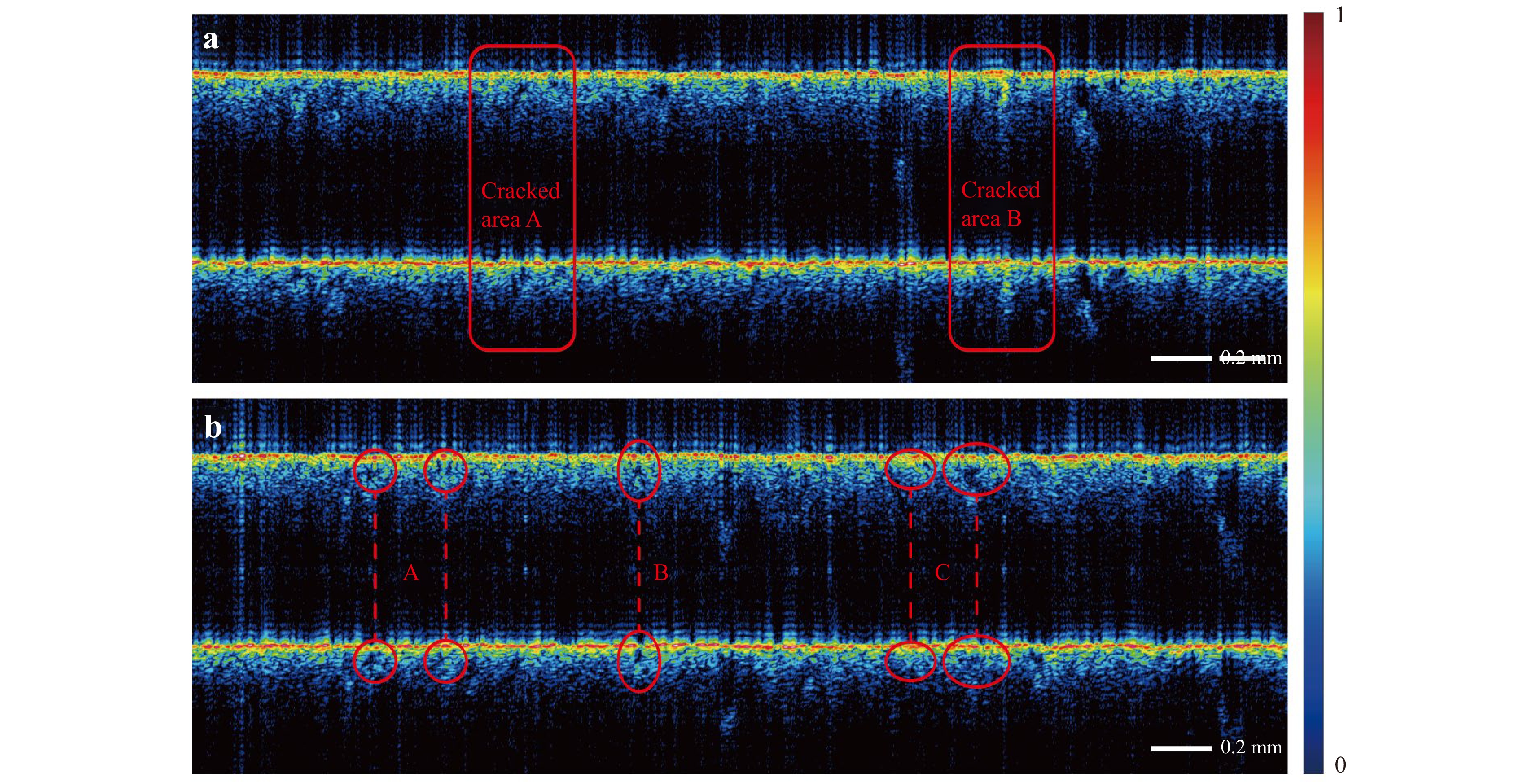
Fig. 8 a In the simultaneous imaging of bright- and dark-fields, although at different positions of the same sample, due to the differences in the illumination of the beam and the collection angle of photons, there are two forms of SSD image morphology: similarity and difference. The marked cracked areas A and B represent the similarity of SSD. b Differences in bright- and dark-field synchronised tomographic image.
-
This study has addressed the challenges of SSD detection in SiC components, particularly RB-SiC, during processing, in which traditional inspection methods are either destructive or inefficient. A non-destructive testing method based on an off-axis BADF-OCT system was proposed. The system integrates a broadband light source, fibre array spectrometer, and off-axis illumination/detection configuration to achieve high-resolution imaging with lateral resolution better than 5 μm and axial resolution better than 1.5 μm. It also offers advantages such as a large depth of field, strong anti-interference capability, and high SNR. The experimental results demonstrate that this method not only effectively distinguishes between surface fracture layers and subsurface crack layers, but also enhances defect detection rates and classification accuracy through the synergistic bright-/dark-field mechanism. Compared with existing methods, this system exhibits comprehensive advantages in terms of non-destructive testing, resolution, detection depth, and defect type discrimination. It provides a viable pathway for the quality control of SiC optical components and lays the foundation for expanding OCT technology applications in industrial inspection.
Owing to the highly complex morphology of SSDs, despite our experimental success in distinguishing the structures from those of SiC phases, industrial and intelligent defect identification remains indispensable. In future work, we will develop high-precision, high-speed SSD recognition algorithms based on the off-axis BADF-OCT system to provide stronger technical support for non-destructive SSD detection in SiC.
-
This research was supported by the Jilin Province Science and Technology Development Project (SKL202502022JC); Jilin Science and Technology Development Plan (No. 20240101029JJ); Synchronized high-speed detection of surface shape and defects in the grinding stage of complex surfaces (KLMSZZ202305); High precision wide dynamic large aperture optical inspection system for fine astronomical observation: National Major Research Instrument Development Project (62127901); Ultra-smooth manufacturing technology of large diameter complex curved surface: National Key R&D Program (2022YFB3403405); and Research on the key technology of rapid synchronous detection of surface shape and subsurface defects in the grinding stage of large diameter complex surface: International Cooperation Project (2025010157). This study was also supported by the Key Laboratory of Optical System Advanced Manufacturing Technology, Chinese Academy of Sciences (2022KLOMT02-04).
Off-axis bright- and dark-field OCT for non-destructive subsurface defect detection in silicon carbide
- Light: Advanced Manufacturing , Article number: 60 (2026)
- Received: 13 January 2026
- Revised: 07 April 2026
- Accepted: 08 April 2026 Published online: 11 May 2026
doi: https://doi.org/10.37188/lam.2026.060
Abstract: The exceptional mechanical and thermal properties of silicon carbide (SiC) make it vital for advanced optics; however, its hardness and brittleness cause subsurface defects (SSDs) during machining that impair performance and longevity. Current detection methods remain destructive and inefficient, whereas conventional optical coherence tomography (OCT) struggles with limited penetration, surface scattering interference, and poor defect contrast in this highly scattering material. We propose a non-destructive off-axis bright- and dark-field synchronous OCT (BADF-OCT) method that captures complementary scattered signals at dual angles to enhance weak subsurface feature detection. The broadband 1100–1500 nm near-infrared spectral-domain OCT system provides high axial resolution with adequate SiC penetration. Experimental validation on reaction-bonded SiC demonstrates clear discrimination between surface fracture and subsurface crack layers, providing reliable detection of micrometre-scale defects at depths up to ~200 μm. Three-dimensional volumetric imaging combined with bright/dark-field data fusion effectively distinguishes true SSDs from surface contaminants, significantly improving the recognition accuracy. This study is expected to contribute to the development of high-energy lasers, large-scale scientific facilities for light sources, and advanced optical manufacturing.
Research Summary
Off-Aaxis Bright- and Dark- Field OCT for SiC SSD Imaging
A method for simultaneously acquiring both the off-axis illumination and photon collection of the bright- and dark-field OCT image was applied to the SSD of SiC. The OCT signal has differences in the returned signals of different media, enabling the acquisition of multi-angle and multi-dimensional morphology of the silicon phase and SSD beneath the RB-SiC surface. In a recent study by Yukun Wang and his team from the Changchun Institute of Optics, Fine Mechanics and Physics of the Chinese Academy of Sciences, they demonstrated the development of an off-axis bright- and dark-field synchronous imaging OCT system, capable of achieving 200 μm imaging beneath the RB-SiC surface. Through the off-axis optical paths that are both illuminating and collecting, dual reference arms, they achieved synchronous acquisition of high axial resolution and high lateral resolution bright-dark-field SSD images.
Rights and permissions
Open Access This article is licensed under a Creative Commons Attribution 4.0 International License, which permits use, sharing, adaptation, distribution and reproduction in any medium or format, as long as you give appropriate credit to the original author(s) and the source, provide a link to the Creative Commons license, and indicate if changes were made. The images or other third party material in this article are included in the article′s Creative Commons license, unless indicated otherwise in a credit line to the material. If material is not included in the article′s Creative Commons license and your intended use is not permitted by statutory regulation or exceeds the permitted use, you will need to obtain permission directly from the copyright holder. To view a copy of this license, visit http://creativecommons.org/licenses/by/4.0/.

 DownLoad: