






-
Photodetectors (PDs) are core components in contemporary optoelectronic technologies, enabling applications ranging from data transmission to health monitoring and smart wearable devices1–3. Conventional PDs are typically fabricated from inorganic semiconductors, such as InN, ZnO, Si, or GaAs, owing to their outstanding optical and electrical properties4–8. However, these materials require complex fabrication processes and high processing temperatures, and are generally incompatible with large-area, flexible, and low-cost manufacturing9,10. These limitations have driven the search for alternative semiconductors that combine outstanding optoelectronic performance with ease of fabrication. Over the past several years, metal halide perovskites have emerged as strong candidates for next-generation optoelectronics, including light-emitting diodes (LEDs), solar cells, and PDs, because of their facile solution processability, strong optical absorption, tuneable bandgap from UV to NIR, long carrier lifetime, and high mobility11,12. Notably, perovskite PDs can operate under zero external bias, that is, in self-powered mode, utilising their own photodiode structure to operate in a self-biasing mode13, which can reduce the power demand for low-powered Internet of Things (IoTs) devices and eliminate the need for batteries. There have been many reports on self-powered perovskite PDs based on single crystals14,15, polycrystalline materials9,16,17, and nanostructures18–23. The solution-processing polycrystalline perovskite PD based on CH3NH3PbI3-xClx films using the p-i-n configuration was developed early by Dou et al., and exhibited a high detectivity of 1014 Jones and fast response times of 180 ns (rise) and 160 ns (fall)24. Subsequently, numerous studies have reported high-performance PDs based on CH3NH3PbI3 perovskite operating in a photodiode configuration25–29. Despite these favourable results, CH3NH3PbX3 perovskite lacks stability. Therefore, mixed-cation compositions have been introduced to improve both the structural and thermal stability without sacrificing performance30. Adam et al. reported triple-cation perovskite PDs fabricated via antisolvent bath extraction, delivering a specific detectivity of 8.8 × 10¹² Jones, a responsivity of 0.52 A·W−1, an on/off ratio of 7.3 × 10⁵, and fast response times of 19 μs (rise) and 21 μs (fall)9. Koth et al. demonstrated an external quantum efficiency (EQE) of 65.30%, a responsivity of 0.30 A·W−1, a specific detectivity of 6.82 × 1012 cm·Hz1/2·W−1, and rise/fall times of 70/88 µs via multi-layer perovskite absorber stack design from low-cost spray coating31. Owing to their high tolerance to environmental stability, triple-cation perovskites are also compatible with scalable coating methods, such as slot-die32 and roll-to-roll printing33.
Meanwhile, all-inorganic perovskites such as CsPbBr3 have gained attention for their superior thermal stability and excellent spectral selectivity in the short-wavelength region34. However, the poor solubility of CsPbBr3 perovskite in N, N-dimethylformamide (DMF) or dimethyl sulfoxide (DMSO) results in poor surface morphology and degraded device performance35. To overcome this challenge, alternative approaches such as microcrystals19, nanowires20, and single crystals36,37 have been developed for PD devices. Wang et al. reported a self-powered PD based on a CsPbBr3 perovskite nanonet with a hollow vertical framework, achieving an on/off ratio of 4.17 × 10⁴, a detectivity of 7.44 × 10¹¹ Jones, and rise/fall times of 0.10/0.16 ms38. Li et al. incorporated ZnO nanoparticles into CsPbBr3 film to enhance the photoresponse of a PD device without external bias voltage, achieving response times of 0.409 s (rise) and 17.92 ms (fall), and an on/off ratio of 12.8635. Zhou et al. used a CsPbBr3 microcrystal to avoid the high defect density of its polycrystalline counterparts and achieved PD performance with a spectral detectivity of 4.8 × 10¹² Jones, a responsivity of 0.172 A·W−1, and on/off ratios of up to 1.3 × 10⁵ at a 0 V bias voltage.19 More recently, Xiao et al. fabricated high-quality CsPbBr3 perovskite nanowire films passivated with ionic liquid 1-octyl-3-methylimidazolium hydrogen sulphate (OMIMHSO4), achieving a responsivity of 0.385 A·W−1 and high detectivity of 7.09 × 10¹³ Jones with very low dark current20. Although these strategies yield excellent device performance, their fabrication routes are impractical for large-scale production.
In general, PDs are categorised as narrowband or broadband, according to the width of their optical wavelength response range. Broadband perovskite PDs typically respond to a wide spectral range, which limits their ability to distinguish light at specific wavelengths. In recent years, selective light detection in PD, which enables the device to distinguish specific wavelengths of light with a narrow spectral range, has been used for many applications, including solar blind and optical communication39,40, AI-based machine vision41–43, imaging, and sensing44–46. For selective light detection purposes, a direct method using absorptive optical filters on broadband PDs leads to fabrication complexity47 and a higher probability of interference from unwanted artefacts48. Another effective strategy is internal filtering, in which broadband-absorbed photons outside the target band are dissipated within the active layer, resulting in wavelength-specific detection. In this case, the narrowband detection is governed by the charge-collection narrowing effect, in which the thickness of the perovskite absorber controls the carrier collection depth. This mechanism sets the onset and switch-off wavelengths, thereby limiting the response of the device to a specific spectral window across the UV-visible (UV-Vis) range49,50. Although this method is effective, the requirement of a high driving bias voltage and a micrometre-thick absorber layer makes it unsuitable for practical usage. Another strategy is to employ perovskite materials with intrinsically narrow spectral absorption and ultrawide bandgaps such as MAPbCl351,52 and low-dimensional triple-cation perovskite (PEA)2(CsxMA0.61-xFA0.39)39(Pb)40(Cl0.88-0.32xBr0.12+0.32x)121.53 However, this strategy is limited to selective detection in the visible range because perovskites naturally absorb across a broad spectral range in this regime. Another possible strategy to improve selective light detection is the utilisation of perovskites with different band energies to create a graded energy band structure, thereby enhancing the specific light absorption. However, a proper combination of perovskite materials with specific band energies is required to enable smooth carrier flow. A previous study demonstrated a triple-cation perovskite PD with an enhanced detection speed via a sequential spray deposition technique to engineer a graded energy band structure from an additional heterojunction between two planar perovskite materials31.
In this study, we developed a novel perovskite stack chocolate-chip-cookie structure as an energy-selective broadband photocurrent amplifier to enhance the responsivity in a target wavelength range. The main objective of this study was to combine two perovskite materials with different bandgaps to generate more current and increase the overall current flow by absorbing the targeted wavelength region. CsPbBr3, a high-bandgap material, can absorb high-energy wavelengths shorter than 540 nm and transfer this energy to the triple-cation perovskite (Cs0.05FA0.81MA0.14Pb (I0.85Br0.15)3) base layer, which can harvest more photon energy from both direct absorption and perovskite-perovskite energy transfer. Considering potential scalability, slot-die coating54 was utilised to deposit triple-cation perovskite (Cs0.05FA0.81MA0.14Pb (I0.85Br0.15)3) as a base-cookie layer, which was intended for internal charge transfer and final transportation to the electrodes. Wide-bandgap polycrystalline perovskite CsPbBr3 droplets were embedded in the form of chocolate chips by spraying to absorb high-energy photons sensitively and transfer such energy to the triple-cation perovskite base layer. The nature of the spray coating, along with the careful annealing strategy, provided homogeneous and discrete microdroplets that spread throughout the base layer. The developed PD achieves improved photocurrent responses at specific wavelengths, such as 532 nm (green) or 365 nm (UVA), because large-bandgap chips effectively trap shorter wavelengths. As opposed to conventional PD optimisation strategies that aim to minimise dark current and maximise detectivity for overall device performance improvement, the novelty of the chocolate-chip-cookie structure is the introduction of enhanced optical interaction within the absorber layer to enhance photocarrier generation at targeted wavelengths via an optical-scattering-induced electric-field redistribution and carrier-funnelling mechanism.
-
The hybrid perovskite fabrication process is illustrated in Fig. 1. For the underlying base layer, a triple-cation perovskite was deposited on an fluorine-doped tin oxide (FTO)/tin(IV) oxide (SnO2) substrate via slot-die coating. To achieve optimal performance, a series of slot-die experiments was conducted to determine the optimal slot-die coating parameters listed in Table S1 (Supporting Information). The average roughness of the slot-die-coated triple-cation perovskite surface was approximately 49.32 nm, as confirmed by the 3D profiler and atomic force microscopy (AFM) topography images shown in Fig. S1a,b (Supporting Information). After setting the base layer, the top-embedded perovskite (CsPbBr3) was sprayed using an airbrush under the optimal conditions adapted from our previous work31. Only the airbrush speed, which is the moving speed of the airbrush relative to the substrate during spray coating, was varied in this study. Before depositing the embedded perovskite droplets onto the base layer, the spray coverage was confirmed by testing the depositions on the FTO substrate at various speeds, as shown in Fig. S2 (Supporting Information). The film appearance and surface coverage at 2–10 mm·s−1 are shown in Fig. S2a (Supporting Information). Because our purpose was to deposit droplets partially as chocolate chips, and not chocolate coatings, 2 mm·s−1 with complete coverage was not suitable. In the UV-Vis spectra shown in Fig. S2b (Supporting Information), all of the sprayed CsPbBr3 perovskite films had an absorption edge at approximately 540 nm, confirming the successful deposition of CsPbBr3 perovskite. The absorbance decreased with an increasing spray speed owing to the decreasing number of spray droplets. Beyond 10 mm·s−1, the spray speed did not produce a sufficient CsPbBr3 peak. Therefore, spray speeds of 4–10 mm·s−1 were selected for further experimentation. To control the droplet distribution carefully, the spray speed and deposition duration were maintained constant during device fabrication to ensure reproducibility. In this process, the timing of the spray during annealing was crucial for the formation of the chocolate-chip-cookie film. While the control triple-cation perovskite film was annealed continuously until it was fully dried, the chocolate-chip-cookie film involved spraying CsPbBr3 perovskite droplets after 5 min of annealing. This timing was critical because, even though the triple-cation film turned black within seconds, it was still partially wet owing to the residual solvent beneath the surface. This semi-wet condition allowed the subsequently applied CsPbBr3 droplets to be embedded into the soft triple-cation matrix, similar to dropping rocks onto a semi-wet mud surface. Following extensive screening, the CsPbBr3 perovskite chips were sprayed onto a slot-die-coated triple-cation perovskite cookie-based layer, as illustrated in Fig. 1.

Fig. 1 Schematic of hybrid perovskite fabrication process.
Fig. 2a, b and S3 (Supporting Information) show the scanning electron microscopy (SEM) cross-sectional images of the pristine cation perovskite layer and hybrid perovskite with average film thicknesses of 812 and 833 nm, respectively. The inset images in both figures show the morphologies of the as-fabricated control triple-cation perovskite and hybrid perovskite. As can be clearly observed for the hybrid perovskite, CsPbBr3 spray droplets were spread homogeneously over the triple-cation perovskite surface. The SEM cross-section confirmed that the CsPbBr3 spray droplets were well embedded inside the bulk of the triple-cation perovskite layer. Fig. 2c shows the size distribution of the CsPbBr3 droplets embedded in the hybrid perovskite film. The droplets exhibited a broad distribution with an average size of 16.27 µm. Despite the broad distribution owing to the spray deposition process, the droplets remained well dispersed within the perovskite matrix. To confirm the phase of the hybrid perovskite film, X-ray diffraction (XRD) patterns are shown in Fig. 2d. It can be clearly observed that almost all of the diffraction peak locations were identical to those of the control triple-cation perovskite phase. Small intensities of the PbI2 peak were observed in all hybrid perovskites at 12.77º. Active CsPbBr3 diffraction peaks at 15.31º (100), 21.72º (110), and 30.78º (200) were also observed in the CsPbBr3 reference film with a dominant (200) plane, indicating a room-temperature stable orthorhombic γ-phase. Surprisingly, two derivative non-photoactive phases of CsPbBr3, such as CsPb2Br5 and Cs4PbBr6, were not observed at 11.7º (002) and 21.8º (104)55–57. All hybrid samples had the preferred (100) crystal plane at 14.18º. Small shifting to a higher 2θ angle was also observed in all hybrid films, as shown in Fig. S4 (Supporting Information). Moreover, the main triple-cation perovskite peaks at 14.18º, 20.10º, 24.63º, 28.48º, and 31.95º, which represent the (100), (110), (111), (200), and (210) planes, respectively, were increasingly broader with a decreasing spray speed. To understand the peak broadening, the Williamson-Hall strain calculation was performed following Eq. 1,
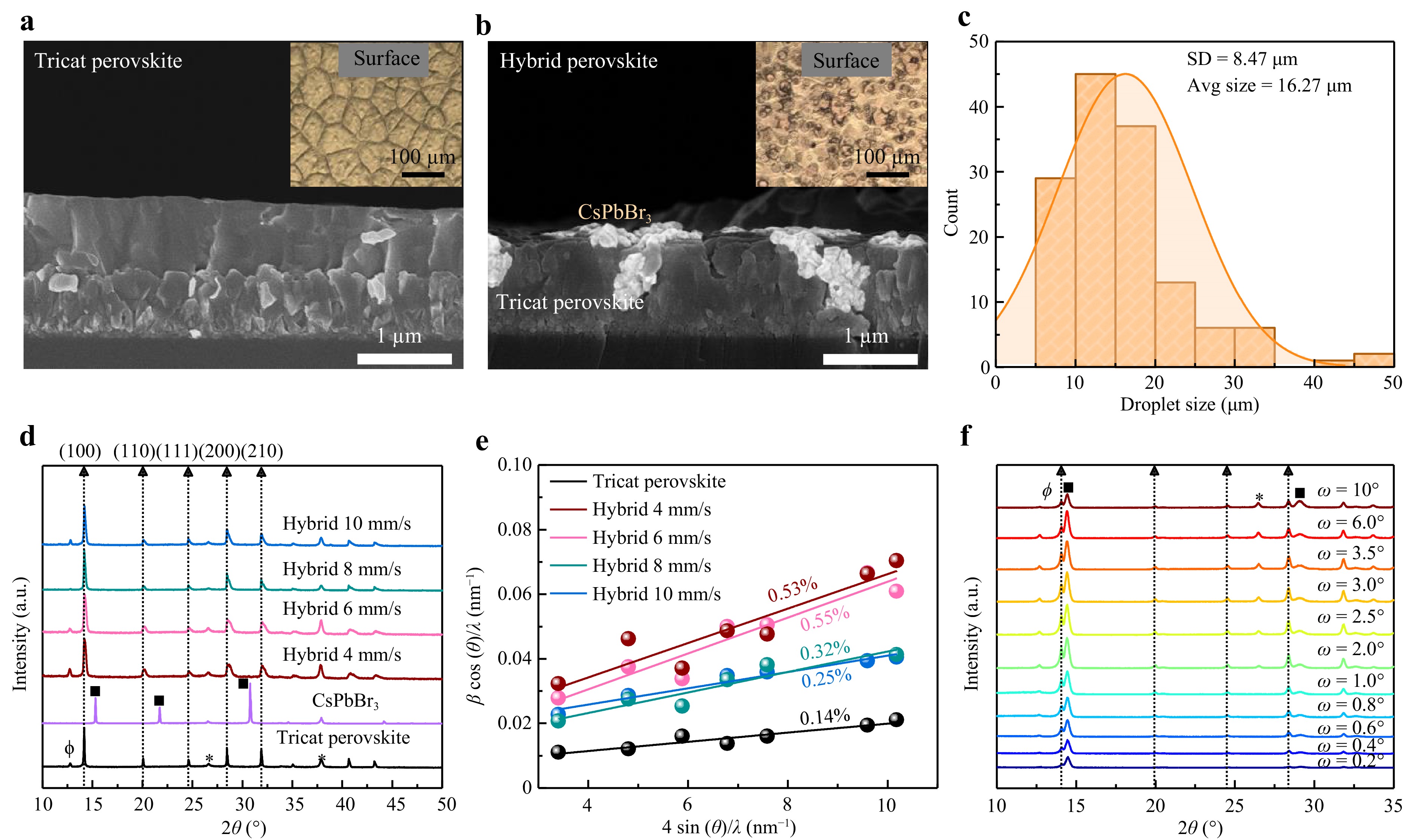
Fig. 2 SEM cross-sectional images of a triple-cation (average thickness = 812 nm) and b hybrid (average thickness = 833 nm) perovskite films (inset: microscope image of respective film surfaces). c CsPbBr3 droplet size distribution histogram (droplet diameters were measured from the microscope image using the ImageJ software). d XRD spectra of triple cation, CsPbBr3, and hybrid (4–10 mm·s−1) perovskites. e Williamson-Hall strain plots of triple-cation and hybrid (4–10 mm·s−1) perovskites. f GI-XRD spectra of hybrid perovskites with different grazing angles (ω) ranging from 0.2°–10° (dotted arrow lines indicate active triple-cation perovskite, ■ = active CsPbBr3, ϕ = PbI2, and * = FTO).
$$ {\beta \cos\theta =4\varepsilon \sin\theta +\frac{K \lambda}{D}} $$ (1) where λ is the X-ray wavelength (nm), θ is the diffraction angle (°), β is the full width at half maximum of the diffraction peak (radians), D is the crystallite size of the perovskite crystal (nm), and K is shape factor (0.9). According to the Williamson-Hall plot in Fig. 2e, higher values of micro-strain were observed with a decreasing airbrush speed, as higher amounts of droplets infiltrated the underlying triple-cation perovskite, which tensed up the perovskite lattice58. The higher the number of chocolate chips (CsPbBr3 droplets), the higher the micro-strain inside the underlying cookie (triple-cation perovskite layer). To reveal the existence of CsPbBr3, grazing incidence X-ray diffraction (GI-XRD) measurement was performed at different grazing incident angles (ω) ranging from 0.2° to 10°, as shown in Fig. 2f. The characteristic diffraction peaks of CsPbBr3 appeared at 14.45° (100) and 29.08° (200), adjacent to the (100) and (200) plane peaks of the triple-cation perovskite, respectively. The peaks were shifted by approximately 0.86° and 1.70° to lower 2θ angles relative to the reference CsPbBr3 positions at 15.31° and 30.78°; the shift was likely attributable to micro-strain and ion exchange owing to the localised interfacial dissolution between the CsPbBr3 droplets and surrounding triple-cation perovskite matrix, where an I− and Br− mixed phase could be created59. Moreover, the preferred crystallographic orientation of CsPbBr3 changed from (200) to (100) compared with that of the standalone CsPbBr3 film. Hidalgo et al. reported that the precursor solvent and A-site cations strongly influence the crystallographic orientation of lead bromide perovskites60. In particular, MA and FA cations promote preferential growth along the (100) plane because of their lower surface energies, making them thermodynamically more stable. Accordingly, the observed shift in the preferred orientation can be explained by the A-site cation exchange at the interfacial interaction region between CsPbBr3 and the surrounding triple-cation perovskite matrix, where the (100) direction growth became energetically more favourable than that of the (200) direction upon chip/cookie contact60. The CsPbBr3 diffraction peak intensity was stronger than that of the triple-cation perovskite. The stronger diffraction peaks of CsPbBr3 arose from its highly ordered crystalline nature57,61 and the use of DMSO as a solvent60, in contrast to the reduced crystallinity of the triple-cation perovskites caused by lattice distortion53,62. Notably, CsPbBr3 peaks were detected across all ω values (all depth profiles) from the surface (ω = 0.2º) to the bulk (ω = 10º), consistent with the cross-sectional images in Fig. 2a, b, where the CsPbBr3 droplets were spread well vertically and horizontally while being embedded inside the triple-cation perovskite layer.
To understand the surface chemical composition of the hybrid perovskites further, X-ray photoelectron spectroscopy (XPS) measurements were performed using a synchrotron radiation source. XPS measures the top approximately 1–10 nm of a material by detecting the kinetic energy (EK) of photoelectrons emitted upon X-ray irradiation. From EK, the corresponding binding energy (EB) of an electron can be calculated using Eq. 2:
$$ E_{\rm B}=hv-E_{\rm K}-\phi $$ (2) in which hν is the photon energy and ϕ is the reference material work function. In general, an increased electron density around an atom enhances the EK of the photoelectrons emitted from its core levels owing to the weaker electrostatic attraction of the nucleus; hence, the EB of the corresponding atom is downshifted in the XPS spectrum63. The XPS spectra of the key elements (Cs 4d, Pb 4f, I 3d, and Br 3d) for the hybrid CsPbBr3/triple-cation perovskite are shown in Fig. S5 (Supporting Information). Notably, the Cs 4d peak of the triple-cation perovskite was not observed because of the detection limit. Compared with the control triple-cation perovskite film, the hybrid perovskite exhibited higher intensities for Cs 4d, Pb 4f, and Br 3d, whereas the I 3d intensity was slightly reduced. This suggests that the surface region of the hybrid perovskite film became relatively enriched in Cs, Pb, and Br species and showed a slight depletion of surface I owing to partial coverage of CsPbBr3 chips. This is in agreement with the GI-XRD data in Fig. 2f, where both CsPbBr3 and triple-cation perovskite could be identified at low ω values (close to the top perovskite surfaces). Importantly, all core levels were systematically shifted to higher EB values compared with those of the triple-cation perovskite; specifically, I 3d5/2 (616.3 → 621 eV), followed by Pb 4f5/2 (136.3 → 139.8 eV) and Br 3d3/2 (66.7 → 69.6 eV). Such upshifting was also observed compared with CsPbBr3; specifically, Cs 4d3/2 (75.4 → 77.5 eV), Pb 4f5/2 (138.1 → 139.8 eV) and Br 3d3/2 (68.3 → 69.6 eV). This type of global upshifting across different core levels is typically described as a rigid electronic shift, which indicates the movement of the Fermi level position relative to the vacuum level64,65. That is, band bending occurs owing to charge redistribution at the interface of the two perovskites, which makes the local chemical environment more electron deficient, resulting in EB upshifting. In perovskite, energy level shifting is mostly related to lead-halide framework modification, whereas A-site cations primarily influence the lattice stability and octahedral tilting66. In our hybrid perovskite, the I 3d shifting was the strongest, followed by Pb 4f and Br 3d, indicating that the integrity of the Pb-I framework of the triple-cation perovskite was strongly perturbed by the incorporation of incoming Br-rich CsPbBr3 droplets, resulting in local I/Br ion exchange, thereby modifying the interfacial electronic structure. This is further supported by a previous study that demonstrated that halide anion exchange strongly modulates valence band evolution and band bending in 2D/3D perovskite heterostructures67.
As shown in Fig. 3a, the absorption edges of the hybrid perovskite peaks were blue shifted with the embedded CsPbBr3 droplets. In addition, the hybrid perovskite film exhibited higher absorption than the triple-cation film at wavelengths longer than 540 nm. This enhancement originated from the formation of Cs/Br-rich phases in the interfacial dissolution region between the CsPbBr3 ‘chips’ and triple-cation ‘cookie’ matrix. Importantly, this increased absorption did not arise from the CsPbBr3 phase itself, but rather from these Cs/Br-rich interfacial regions that were generated during the chip-cookie interaction. The region of interest was the wavelength range beyond 540 nm, where CsPbBr3 was photoactive. As shown in the inset of Fig. 3a, the absorption of the hybrid perovskite in that region increased with more spray droplets and a lower airbrush speed because of the co-absorption mechanism, where CsPbBr3 droplets absorbed light at wavelengths near their absorption onset in addition to the broad absorption by the underlying triple-cation perovskite. Steady-state photoluminescence (PL) measurements were performed to understand the charge-transfer dynamics of the hybrid perovskite, as shown in Fig. 3b. A 450-nm high-power LED was used as the excitation source to excite both perovskite materials inside the hybrid perovskite. As the perovskite layers for PL measurements were deposited onto the electron transport layers (ETLs), sequential PL quenching was observed under all hybrid perovskite conditions from 4 to 10 mm·s−1. In principle, PL quenching may originate from either trap-assisted non-radiative recombination or interfacial charge transfer68,69. If the trap states were dominant, the hybrid perovskite fabricated at the lowest spray speed (4 mm·s−1), which corresponded to the highest droplet population, would be expected to show the weakest PL owing to the greatest probability of surface defect formation. However, our measurement results revealed the opposite trend, in which the 4 mm·s−1 hybrid perovskite displayed the strongest PL signal, and the PL intensity decreased consistently as the spray speed increased (decreasing droplet population). Specifically, this observation confirmed that an excessive number of droplets at this spray speed caused the merging of CsPbBr3 chips to become an unwanted full layer, which blocked charge transfer, as discussed previously. In contrast, the PL quenching in the hybrid perovskites with an increasing spray speed was primarily governed by the interfacial charge-transfer mechanism that accelerated charge extraction, thereby reducing radiative recombination, in agreement with previous reports31,69. This observation was further supported by the XPS results, in which the systematic global upshifts revealed significant charge redistribution and band bending at the chip/cookie interfaces. Similar to the UV-Vis spectra, blue shifting could also be observed in the PL spectra of all hybrid perovskites, as shown in Fig. 3b (inset). The shifting was more obvious with a decreasing spray speed, which can be attributed to the introduction of more Cs- and Br-rich phases59 at the chip/cookie interfacial dissolution regions, which was consistent with the above GI-XRD peak shifts at all depth profiles and significant increases in the XPS intensities (Cs 4d, Pb 4f, and Br 3d).
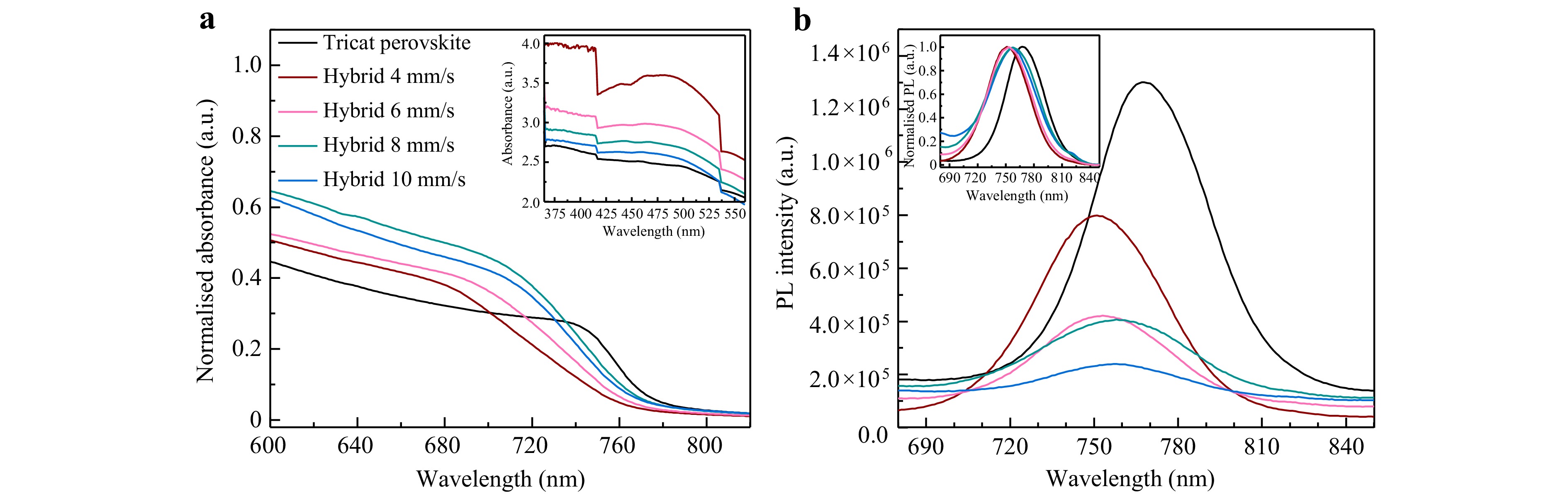
Fig. 3 a UV-Vis spectra of control triple-cation and hybrid perovskite films (inset: zoomed in absorption range from 560–365 nm). The artificial step-like absorption spectrum in the inset arose the error from the detector switching in our UV-Vis equipment. b Static PL spectra of control triple-cation and hybrid perovskites (4–10 mm·s−1) (inset: normalised intensities of PL spectra).
To support the charge-transfer concept within the hybrid perovskite, UV photoelectron spectroscopy (UPS) energy-band measurements from synchrotron light under vacuum conditions were performed separately for the two perovskites. Fig. S6 (Supporting Information) shows the fitted raw UPS data for both perovskites, and Table S2 (Supporting Information) shows the calculated energy-band information extracted from the UPS data analysis. Fig. 4a illustrates the possible energy-band diagram of the hybrid perovskite under noncontact conditions. It should be noted that the energy band data of SnO2 and spiro-OMeTAD were obtained from a previous study70. According to the band structure diagram, a type-I (straddling) heterojunction was formed between the triple-cation perovskite and CsPbBr3 perovskite. This type of band structure is of interest because we wish to utilise the ability of wide-bandgap materials to boost the sensing ability in a specific wavelength range, while the underlying layer can be used to facilitate charge transfer. However, this type of band structure is primarily used for LED-related applications owing to its high radiative recombination71. Our hybrid perovskite was intentionally designed to reverse this effect. Two likely scenarios exist. In the typical layer-by-layer structure, CsPbBr3 fully covers the top surface of the triple-cation perovskite base layer, which is blocked by CsPbBr3 and trapped at the interface owing to type-I band alignment, resulting in increased radiative recombination. In our chocolate-chip-cookie structure, CsPbBr3 is embedded as droplets (chips) in the triple-cation perovskite host material (cookie). Because this host material maintains direct contact with both the ETL and hole transport layer (HTL), it provides an uninterrupted pathway that allows charges that are generated within the hybrid perovskites to flow efficiently to the collection layers and increases the overall current flow, which is the so-called reverse type-I concept. Fig. 4b, c illustrate the charge-transfer direction in the control and hybrid perovskite devices, respectively. When light shone upon the device, the Fermi level became aligned, while band bending occurred between each junction. The photogenerated charge carriers from the active layers were then separated into their respective charge-transport layers by drift and diffusion mechanisms owing to the development of the depletion region72. As can be observed from Fig. 4b, electrons and holes from the triple-cation perovskite could transfer fluently to the ETLs and HTLs, respectively, as the triple-cation perovskite made direct contact with both transport layers. However, in Fig. 4c, the electrons and holes from the CsPbBr3 perovskite could not jump directly to the SnO2 and spiro-OMeTAD, respectively, because the energy-gap transitions were too large. In theory, the charges jump to the closest energy band first in a stepwise transition. Furthermore, CsPbBr3 was not in direct contact with the ETL in our device stack. Consequently, both the photogenerated electrons and holes from CsPbBr3 must first transit to the triple-cation perovskite, providing additional charges for the device. To support the concept of the charge-transfer process in our hybrid perovskite, a SCAPS-1D simulation was performed, as shown in Fig. S7 (Supporting Information). Although the SCAPS-1D could not fully display the chocolate-chip-cookie structure of the hybrid perovskite, the simulation was performed under 520 nm illumination with varying CsPbBr3 thicknesses (20 and 300 nm) to model the experimental conditions (hybrid 4 and 8 mm·s−1) approximately. As can be observed from Fig. S7 (Supporting Information), the CsPbBr3 thickness significantly influenced the band-bending behaviour, consistent with the XPS results. In the case of 300 nm thickness, obvious upward band bending occurred at the triple-cation perovskite/CsPbBr3 interface, indicating the formation of an internal electric field. This field facilitated efficient electron transport towards the ETL, while hole extraction was blocked by the thick CsPbBr3. Conversely, in the case of 20 nm thickness, the band bending and charge blocking were less pronounced, as the built-in potential was weaker, causing lower open-circuit voltage (Voc) and much higher short-circuit current density (Jsc) in the simulated I–V characteristics compared with those with 300-nm-thick CsPbBr3, as shown in Table S3 (Supporting Information). However, in real cases, a better Jsc is expected owing to the extended triple-cation perovskite/CsPbBr3 contact throughout the absorber layer, as demonstrated by the GI-XRD, without the cost of a lower Voc because the chip/cookie arrangement allows direct contact between the triple-cation perovskite and HTL, unlike the simplistic models described above.
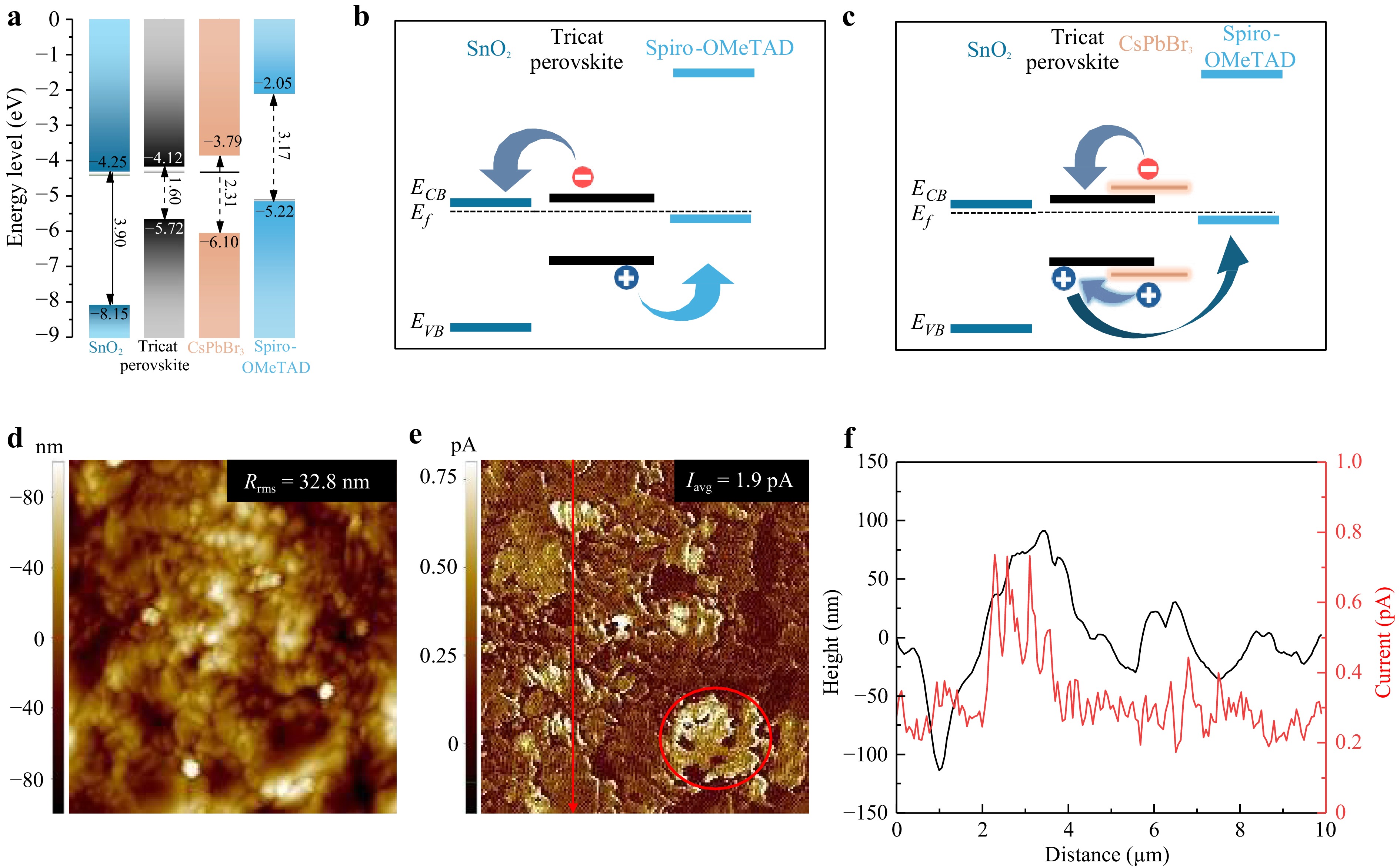
Fig. 4 a Band structure of hybrid perovskite device under non-contact conditions with respect to vacuum. Possible charge-transfer direction in b control and c hybrid perovskite devices under contact conditions (Fermi level aligned). d AFM surface topography and e c-AFM current mapping of hybrid perovskite under 532 nm wavelength irradiation (green, the circle area = CsPbBr3 chip). f Height and current profiles of the denoted line in d.
The surface roughness was investigated using AFM. Fig. 4d presents the surface topography of the hybrid perovskite with a 10 × 10 µm2 scanned size, showing a smooth surface with a root mean square roughness (Rrms) of 32.8 nm. To reveal the charge generation from both materials of the hybrid perovskite, conductive atomic force microscopy (c-AFM) measurements were performed during irradiation under a 532 nm light wavelength. As shown in Fig. 4e, f, the red highlighted region of CsPbBr3 became a hotspot for more photocurrent generation compared with that of the triple-cation perovskite region with photocurrents of 0.73 and 0.44 pA, respectively, which is strongly indicative of the chip/cookie structure, in agreement with the SEM analysis above. In addition, c-AFM measurements under 656 nm wavelength illumination were performed as a negative control. As shown in Fig. S8 (Supporting Information), in this case, less current generation was detected in the CsPbBr3 region, confirming that the chocolate-chip-cookie structure functions with specific light illumination by design. Thus, the study confirmed our hypothesis that although both materials can generate current under 532 nm emission, the droplets can generate more current and increase the overall current flow.
The sensor performance of the specially designed chocolate-chip-cookie-like hybrid perovskite PD device was measured using the device structure FTO/SnO2 sol-gel/SnO2 NPs/perovskite/spiro-OMeTAD/Au-Ag under 532 nm (green) laser irradiation with a 1 kHz optical chopper, as shown in Fig. 5a. The transient photocurrent response peaks of the hybrid perovskite PDs with different spray speeds under a 532 nm laser with 0 V bias are shown in Fig. 5b. Compared with the control device, all hybrid devices except for the 4 mm·s−1 device showed higher transient photocurrent responses, with the best performance at 8 mm·s−1 under green light illumination, owing to the better green light absorption of CsPbBr3 and positive energy flow from CsPbBr3 to the base perovskite layer. At 4 mm·s−1, the CsPbBr3 layer was thick and possibly covered most of the triple-cation surface area, blocking the charge transfer, as shown in Fig. S7b (Supporting Information). At the low end of 10 mm·s−1, the number of perovskite droplets may not be sufficient. To understand the charge-carrier transfer in the hybrid devices further, the photocurrent rise time (τrise) and fall time (τfall) were analysed. τrise represents the duration for which the photocurrent rises from 10% to 90% of its maximum value upon light exposure, and vice versa for the fall time. Under illumination, electron-hole pairs are generated in the active perovskite layer, whereas band bending occurs between junctions. These generated charge carriers drift towards both electrodes. In general, as illustrated in Fig. 5h, if the internal band alignment of the device is mismatched or it has intrinsic defects, charge transportation becomes impeded while some carriers are trapped; both processes potentially slow the τrise signal. Consequently, inefficient charge extraction leads to a slower τfall signal73. As shown in Fig. 5c-g and S9 (Supporting Information), all of the hybrid perovskite devices except for the 4 mm·s−1 device were slower in τrise values compared with the control device, possibly owing to more interfacial contacts and more occurrences of two-step energy transfer (CsPbBr3 → triple-cation perovskite → HTL). For the 4 mm·s−1 device, τrise and τfall were relatively much slower, as the CsPbBr3 blocked charge transfer between the triple-cation perovskite and HTL, as shown in Fig. S9b,c (Supporting Information)74. However, the τfall values of the hybrid samples were similar to those of the control, albeit consisting of both the fast decay from bulk and the additional slow decay, as indicated by the red arrow from the outflow of the trap filling in Fig. 5e-g.
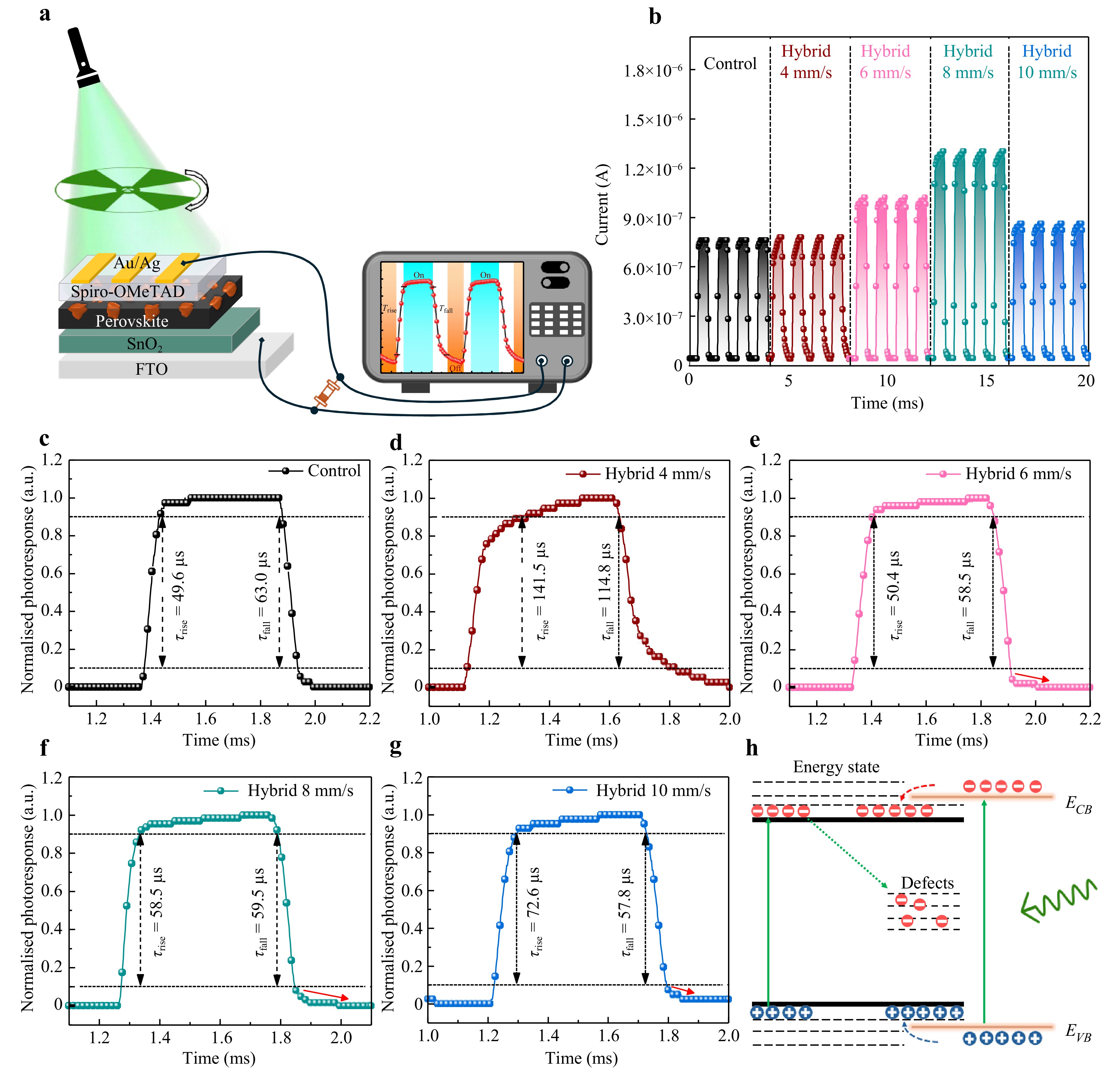
Fig. 5 a Schematic of hybrid perovskite PD device measurement setup. b Photocurrent response of control triple-cation and hybrid perovskite PDs under 532 nm light irradiation with 1 kHz optical chopper. c-g Rise and fall time responses of control and hybrid PD devices with different conditions (4, 6, 8, and 10 mm s−1). h Schematic of charge-carrier generation and extraction mechanism.
To confirm our findings, the dark current and space-charge-limited current (SCLC) were investigated under optimised conditions (hybrid 8 mm s−1). To measure the SCLC, an electron-only pseudo-device was fabricated using an FTO/SnO2 sol-gel/SnO2 NPs/perovskite/PC60BM/Au-Ag device structure, as illustrated in Fig. 6a. The hybrid device showed a higher trap density (Nt = 2.95 × 1015 cm−3) than that of the control device (Nt = 1.50 × 1015 cm−3), as shown in Fig. 6b, which led to a higher measured current density (Jd) of 8.65 × 10⁻⁹ A·cm−2 compared with the 1.66 × 10⁻⁹ A·cm−2 of the control at a nominal 0 V bias (under dark conditions), as shown in Fig. 6c. These traps were responsible for the slow component observed in the photocurrent fall time (τfall). These results are also consistent with the previously discussed micro-strain, increased interfacial area, and localised interfacial dissolution between the CsPbBr3 droplets and surrounding triple-cation perovskite matrix. However, this trade-off was expected to improve the photocurrent detection at a specific wavelength.
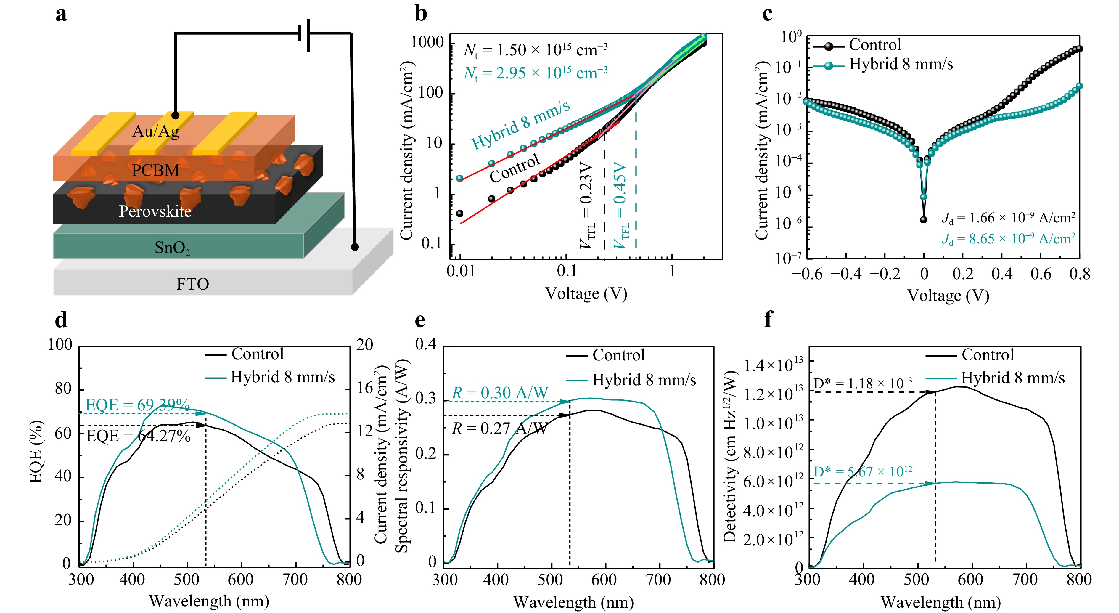
Fig. 6 a Schematic of SCLC measurement device structure. b Trap-state density fitting of SCLC. c J-V characteristics of control and hybrid (8 mm·s−1) devices under dark conditions (see measurement setup in Fig. S10a). d EQE, e spectral responsivity, and f specific detectivity of control and hybrid (8 mm·s−1) devices (all measurements were conducted under 0 V bias; the measurement setup is shown in Fig. S10b).
The EQE determines the number of photogenerated carriers per incident photon. As shown in Fig. 6d, the EQE of the 8 mm·s−1 hybrid device started to generate carriers starting at approximately 760 nm, whereas that of the control device started at approximately 780 nm, in agreement with the UV-Vis result. The EQE of the 8 mm·s−1 hybrid device started to become higher than that of the control device at a wavelength of approximately 700 nm and reached the highest EQE of 73.10% at approximately 460 nm, whereas the control device showed an EQE of 64.13%. Specifically, the EQE increased from 64.27% to 69.39% at 532 nm (~7.9% improvement) and from 43.67% to 47.38% at 365 nm (~8.5% improvement) compared with the control device. The overall photocurrent conversion in the hybrid device demonstrated a broadband nature across the visible spectrum, which was noticeably higher than that of the control device for the specific range of interest, and was influenced by the CsPbBr3 absorption profile. The spectral responsivity (R) indicates how efficiently the device can convert the light of different wavelengths into electrical signal, which is mainly related to the EQE. As shown in Fig. 6e, the R values of the 8 mm·s−1 hybrid device were higher than those of the control at 365 and 532 nm, reaching 0.14 and 0.30 A·W−1, respectively, which was particularly linked to the high photocurrent responses (on/off ratios) observed in the above results. Fig. 6f shows the specific detectivity (D*) of the PD devices, which reflects the performance of the devices in detecting light at a lower intensity without noise interference. D* can be calculated by Eq. 3:
$$ { D}^*={ R}/\sqrt{2qJ_d} $$ (3) where Jd is the dark current density. In general, lowering Jd effectively reduces the noise level and leads to a higher D*31. As expected, the high Jd of the hybrid devices adversely affected their D* values; the control and 8 mm·s−1 hybrid devices showed values of 1.18 × 10¹³ and 5.67 × 1012 cm·Hz1/2·W−1, respectively. Note that the reported specific detectivity values were measured under the thermal-noise assumption based on the characteristics of the device at zero bias; additional low-frequency noise contributions, such as 1/f noise, were not considered. To support the thermal-noise assumption, the spectral density of the current noise was calculated using the Johnson-Nyquist equation, as shown in Fig. S10c (Supporting Information). The values for both the control and hybrid PDs were almost of the same order of magnitude as those in previous studies75–77. Table S4 (Supporting Information) presents a comparison of the hybrid perovskite structure PD device performance with those of previously reported studies. With the trade-off owing to more interfaces, the relative performance was not the main focus of this study. However, the new chocolate-chip-cookie architecture offers an interesting concept, along with photocurrent enhancement, which can be further optimised in the future.
Furthermore, Fig. 7a-d summarises the statistical comparison of the τrise, τfall, on/off ratio, and Jd between the control and 8 mm·s−1 hybrid devices.
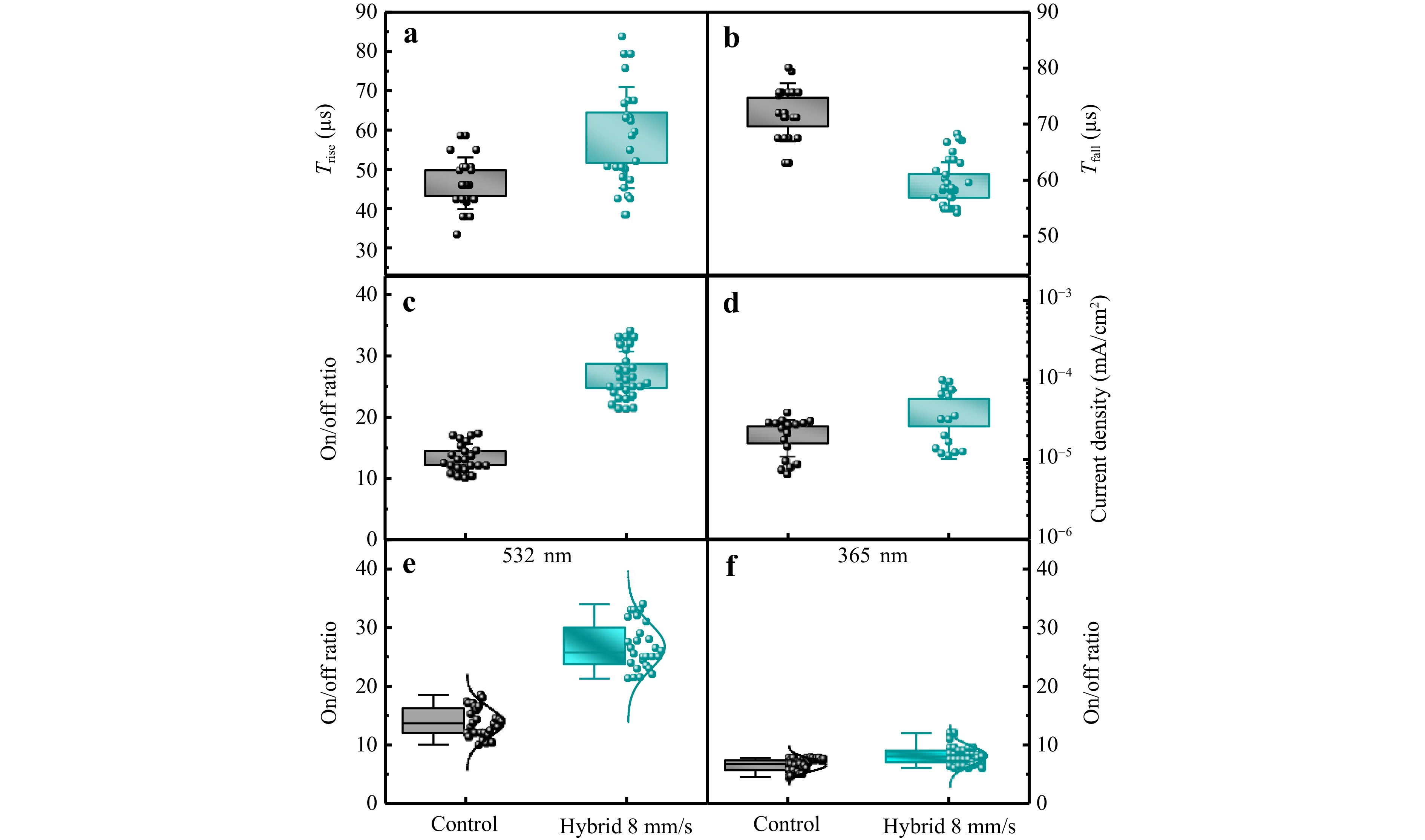
Fig. 7 a 10%–90% of photocurrent rise time (τrise). b 90%–10% of photocurrent fall time (τfall). c On/off ratio and d measured current density (at nominal 0 V bias under dark condition) of control triple-cation and hybrid (8 mm·s−1) perovskites. On/off ratio comparison of control triple-cation and hybrid (8 mm·s−1) perovskites under e 532 nm and f 365 nm light irradiation.
To confirm the enhanced light detection strategy further, the photodetection performance of the hybrid perovskite devices was measured under two different light sources (532 and 365 nm). As shown in Fig. 7e, f, the hybrid devices demonstrated superior performance at both 532 and 365 nm, with a particularly strong photocurrent detection enhancement at 532 nm, in agreement with the EQE results. Although the device maintained broadband sensitivity across the visible spectrum, the hybrid architecture enhanced the photoresponse at specific wavelengths within a range of tens to hundreds of microseconds of rise/fall times. Although this response speed is slower than that required for ultrafast applications, such as LiDAR systems, which typically require nanosecond-scale detection, it remains sufficiently fast for many practical optoelectronic sensing applications, such as UV monitoring sensors, environmental IoT devices, and low-power bioimaging systems.
To gain further insight into the dark current behaviour, time-resolved PL (TRPL) measurements were performed under 635 nm excitation. As 635 nm light does not excite CsPbBr3, the PL response reflected only the charge-carrier lifetime of the triple-cation perovskite, which was influenced by more traps and defects owing to the chip/cookie interfaces. As can be observed in Fig. S11 (Supporting Information), the significantly shorter average lifetime (τavg = 234 ns) for the hybrid 8 mm·s−1 perovskite compared with the 1,040 ns of the control indicated more defects, consistent with the high dark current and trap density in the SCLC measurement. This behaviour is attributed to the additional chip/cookie interfaces, which could introduce localised trap states. Nevertheless, the hybrid structure consistently produced higher photocurrent and responsivity under 365 and 532 nm illumination, indicating that the embedded CsPbBr3 droplets effectively enhanced the photocarrier generation within the absorber layer. In the future, this interesting device concept can be further optimised to reduce the dark current trade-off.
The dependence of the photocurrent on light intensity was further investigated to evaluate the photoresponse behaviour of the devices under different illumination conditions. As shown in Fig. S12a, b (Supporting Information), the photocurrent increased with an increasing light intensity under both 532 nm (green) and 365 nm (UV) illumination for both the control and hybrid devices. This behaviour indicated efficient carrier generation and collection within the PD devices. The hybrid device consistently demonstrated a higher photocurrent than the control device over the entire illumination range. Therefore, the observed improvement under both 532 nm (green) and 365 nm (UV) illuminations followed a similar trend to that observed in the EQE result, further confirming the enhanced photoresponse of the hybrid structure.
To analyse the dynamic response of the PDs further, the linear dynamic range (LDR), which represents the ability of a PD device to maintain a linear photoresponse across a range of light intensities, was calculated using Eq. 4:
$$ LDR=20\log \left(\frac{{J}_{max}}{{J}_{dark}}\right) $$ (4) where Jmax is the maximum measurable photocurrent density under illumination and Jdark is the dark current density. As shown in Fig. S12c, d (Supporting Information), both devices exhibited an increase in the LDR with an increasing illumination intensity, indicating a stable photoresponse across a wide range of incident light intensities. Specifically, under 365 nm illumination, the hybrid device showed an LDR of approximately 102.5 dB at the highest measured intensity, compared with 103.5 dB for the control device, whereas under 532 nm illumination, the hybrid and control devices achieved LDRs of approximately 112.7 and 108.8 dB, respectively. Although the hybrid device did not exhibit a significant improvement in the LDR compared with the control device, this behaviour can be attributed to the relatively high dark current arising from additional interfaces introduced by the embedded CsPbBr3 droplets. Nevertheless, the hybrid PD maintained a comparable dynamic response while delivering an enhanced photocurrent under both UV and green illumination. These results confirm that our chocolate-chip-cookie hybrid structure preserved a reliable light-intensity detection capability across the measured illumination range, despite the slightly higher dark current.
Ansys Lumerical simulations were performed to investigate the underlying photogeneration mechanism as shown in Fig. 8a-f and S14a-d (Supporting Information). Fig. 8a, c show the simulated charge-generation rate profiles of the hybrid and control structures under 532 nm illumination. For the hybrid structure, the charge generation was primarily concentrated near the chip/cookie interface and surrounding matrix, whereas weaker wave-like generation patterns were observed inside the CsPbBr3 chip domains. Less charge-generation rate inside the chip is due to a lower absorption coefficient value. In contrast, the control perovskite exhibited a relatively uniform charge-generation distribution across the film.
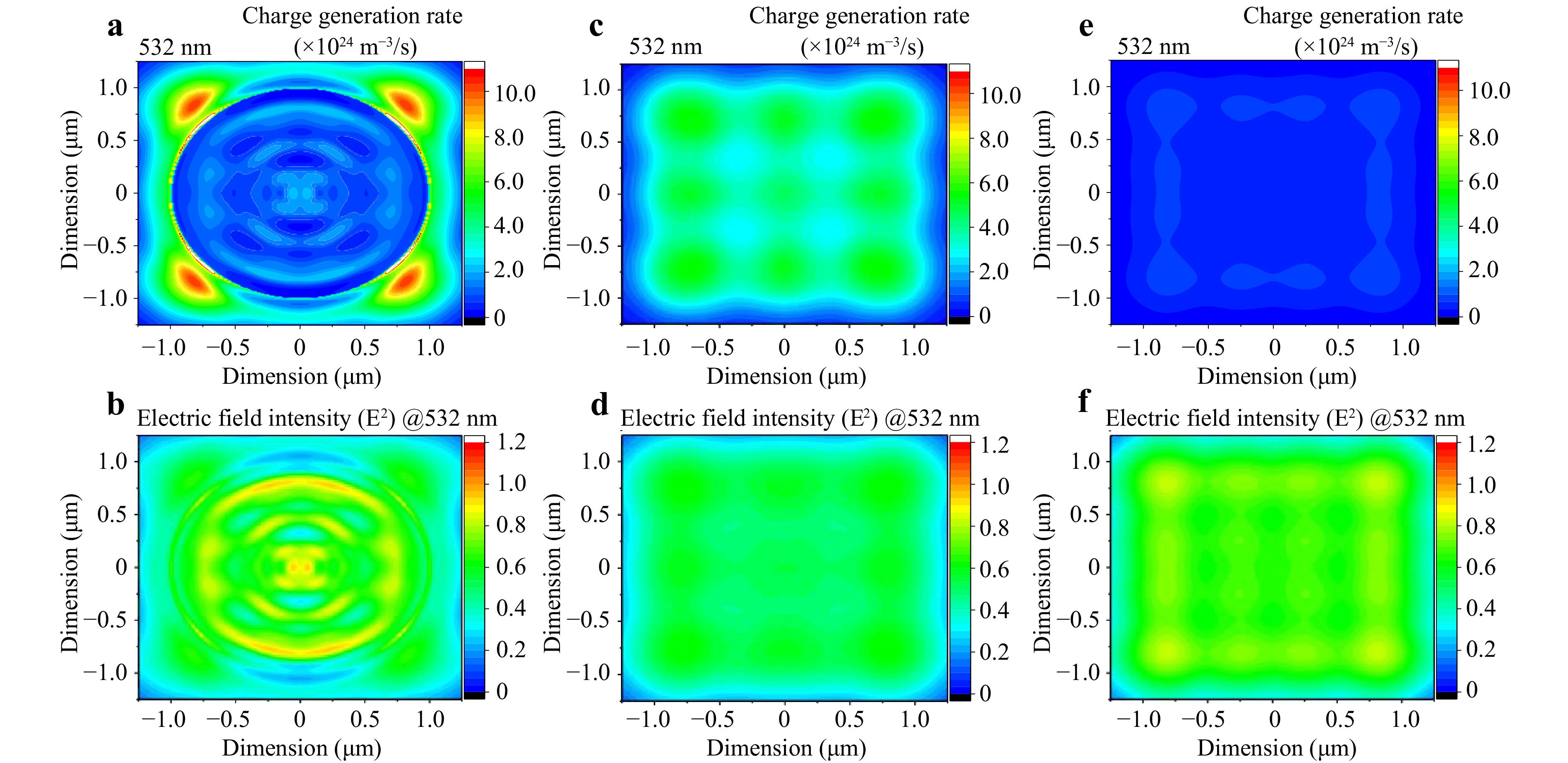
Fig. 8 Ansys Lumerical simulated charge-generation rate and electric field intensity profiles of a, b chocolate-chip-cookie perovskite, c, d control perovskite, and e, f perovskite/perovskite graded structures under 532 nm light illumination (see Fig. S13 for information on simulation models).
To understand this behaviour, the electric-field intensity distribution was also simulated, as shown in Fig. 8b, d. In the control device, the electric field was uniformly distributed throughout the perovskite layer. However, in the hybrid structure, the electric field formed concentric ring-like interference patterns with localised enhancement near the chip/cookie interface. This electric-field distribution is attributed to the scattering and propagation of incident light caused by the refractive index contrast between the CsPbBr3 droplets and triple-cation perovskite matrix. As a result, the CsPbBr3 droplets redistributed the local electric field towards the chip/cookie interface and surrounding matrix, leading to enhanced photocarrier generation in these regions. Meanwhile, the CsPbBr3 droplets also absorbed part of the incident photons and generated carriers within the droplet domains, which appeared as the wave-like generation patterns shown in Fig. 8a. According to earlier discussion, the generated carriers can be spatially directed towards the surrounding triple-cation perovskite matrix, which serves as a continuous carrier transport pathway.
Furthermore, as shown in Fig. S14a (Supporting Information), the overall charge-generation rate increased significantly, and a similar charge-distribution pattern near the chip/cookie interface was observed under 365 nm illumination. In the case of 750 nm illumination, as shown in Fig. S14d (Supporting Information), the electric-field intensity became even stronger than that observed under 532 nm owing to optical scattering induced by the CsPbBr3 chips. However, the corresponding charge generation remained weak because the photon energy was near the absorption edge of the material, where the absorption coefficient was significantly lower. For comparison, a graded heterostructure model consisting of a planar CsPbBr3 layer on top of the dark perovskite was also simulated, as shown in Fig. 8e, f. In this case, both the charge-generation and electric-field maps exhibited a relatively uniform horizontal distribution across the film surface, indicating conventional thin-film optical propagation. In brief, as opposed to the control and planar graded system, the CsPbBr3 droplets inside the developed chocolate-chip-cookie structure functioned both as localised photon absorbers and electric-field redistribution centres, enabling enhanced carrier generation and funnelling pathways towards the dark perovskite matrix, which contributed to the improved photoresponse of the hybrid PD.
Fig. 9a and S15 (Supporting Information) show the cyclic photocurrent response stabilities of the devices measured under periodically modulated illumination at wavelengths of 532 nm (green) and 365 nm (UV) for 600 s to evaluate the operational stability of the PDs. The hybrid device exhibited comparable operational stability to the control device under both 365 and 532 nm illumination by providing reliable and stable on/off switching behaviour throughout the measurement period. A small initial rapid decay in the photocurrent was observed for both devices during the early cycles, which was attributed to the trap-filling process occurring at the beginning of light exposure. Following the trap-filling period, the photocurrent of the hybrid device decreased gradually, retaining approximately 88% of its initial value. In comparison, the control device exhibited a slightly higher stability, retaining approximately 91% of its photocurrent over subsequent cycles. This highly repeatable on/off switching response confirmed the reliability and operational robustness of the hybrid PD. Fig. 9b, c demonstrate the environmental stability testing of the PD devices. Both the control and hybrid devices were tested without encapsulation. Moisture stability was tested within a dry box maintained at 40%–50% relative humidity (RH), whereas the thermal stability was tested at 65 ºC in a glovebox atmosphere. In terms of moisture stability, both the hybrid and control devices exhibited a reduction in the on/off ratio to approximately 50% of their initial values by day 2. Subsequently, the hybrid device demonstrated recovery, reaching approximately 80% of its initial on/off ratio by day 4. The control device recovered only approximately 60% of its initial on/off ratio. However, on day 22, both devices lost approximately 70% of their original performance. Similarly, the thermal stability test revealed a significant reduction in the on/off ratio for both devices, with a substantial loss observed as early as day 2, which remained at only approximately 30% of the initial value. The observed stabilities under both testing conditions suggest that the hybrid structure is as stable as the control one; the degradation is likely attributable to the intrinsic instability of spiro-OMeTAD78 and increased interfacial defects introduced by the embedded CsPbBr3 droplets. Although this study did not primarily focus on stability, this finding highlights the future need for interfacial perovskite passivation materials such as organic ammonium salts79–81, halide salts82,83, 2D-MXene nanosheets84,85, CdS nanorods86, thin polymer layers87, or encapsulation strategies for hybrid perovskite PDs.
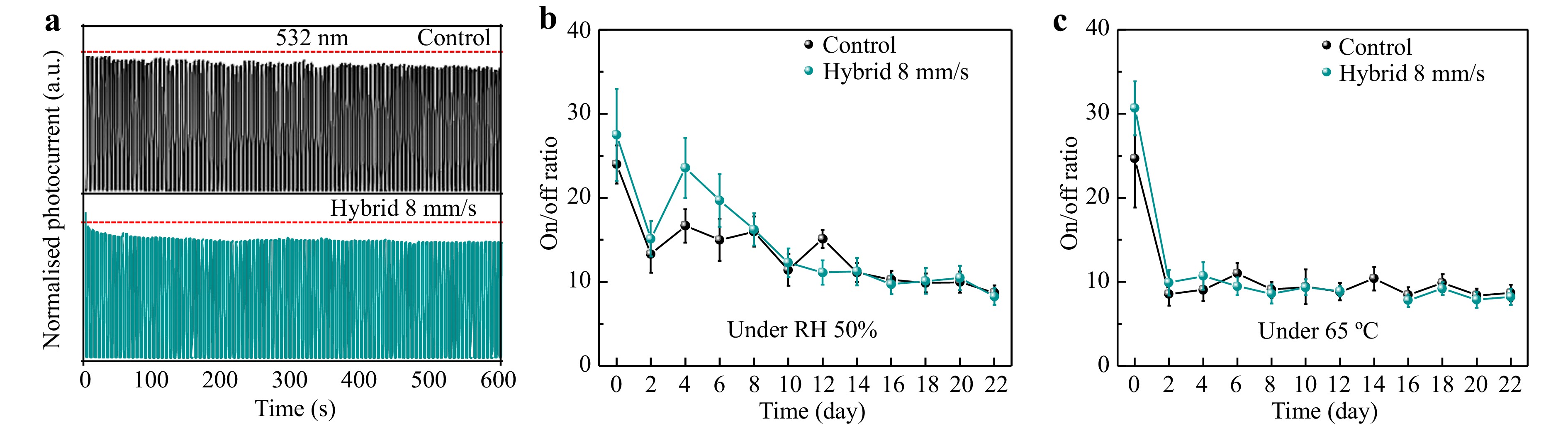
Fig. 9 a Cyclic operational stability (100 cycles, 600 s) under periodically modulated illumination of 532 nm (green). b Moisture stability and c thermal stability comparison of control and hybrid devices without encapsulation (note: data-saving error at day 14 of thermal stability).
To determine the stability of hybrid perovskite film, X-ray diffraction (XRD) measurements were carried out on all the samples stored in three different environments over time: (1) 50% RH, (2) ambient conditions, and (3) 85 °C at different time durations, as shown in Fig. S16 (Supporting Information). Under high-temperature aging, both the triple-cation and hybrid perovskite films exhibited material degradation, as evidenced by the growth of the PbI2 peak at 12.77°. Interestingly, the PbI2 peak in the hybrid perovskite grew faster, indicating that the hybrid perovskite was more vulnerable to thermal degradation. In contrast, under ambient conditions and 50% RH, the hybrid perovskite showed a structural stability comparable to that of the triple-cation film, with no additional degradation peaks observed. Kinetic PL tracing measurements were performed to understand the underlying mechanism of the thermal instability of the hybrid perovskite. The measurements were performed under 450 nm continuous excitation at 120 °C. As can be observed from Fig. S17 (Supporting Information), the PL intensities of both the hybrid and triple-cation perovskites increased gradually over time, with rise time constants of τhybrid = 917.2 s and τtricat = 764.4 s. In a previous report, such an increase in PL intensity under continuous illumination was typically attributed to the light-induced deactivation of non-radiative recombination centres and the thermally assisted redistribution of photoinduced ions in the sublattices88. The longer rise time in the hybrid perovskite indicates that a longer time is required to deactivate the non-radiative recombination centres, suggesting the existence of ion redistribution under optical and thermal stress, and hence, a more defect-rich environment. This explanation agrees well with both the SCLC and dark current results discussed previously. In contrast, the triple-cation perovskite exhibited a smaller PL intensity change and shorter rise time, implying fewer initial traps, a faster deactivation time, and a more intrinsically ordered and stable structure. Despite showing a lower thermal stability, this is not a practical concern because the sensor may not operate at such high temperatures. The functional role of second embedded perovskite was further explored by substituting CsPbBr3 with other wide-bandgap perovskites to investigate the energy-selective photocurrent amplification in the UV range as discussed in Fig. S18.
-
A new strategy for energy-selective broadband amplification of the photocurrent in self-powered mode was introduced by designing a photodiode-based perovskite PD with a chocolate-chip-cookie-like hybrid structure. Embedding wide Eg CsPbBr3 chips into a slot-die-coated triple-cation perovskite matrix resulted in electric-field redistribution centres due to refractive index contrast and energy-funnelling pathways enabled by efficient charge transfer from CsPbBr3 to the triple-cation perovskite, which was proven by multiple experimental results, and later, to the respective charge transport layers. Additionally, Comprehensive structural, optical, and electrical characterisations confirmed the coexistence and interaction of both perovskite materials within the hybrid structure, confirming ion exchange and charge redistribution at the interface. The optimised hybrid device achieved enhanced performance under both green (532 nm) and UVA (365 nm) illumination, with EQEs of 69.39% and 47.38%, spectral responsivities of 0.30 and 0.14 A·W−1, and on/off ratios of 34 and 12, respectively. However, a trade-off between detectivity and responsivity was observed owing to more interfaces. The proposed hybrid device is beneficial for self-powered photodetection applications, including UV monitoring sensors, environmental IoTs devices, and low-power imaging systems. The use of slot-die and spray coatings demonstrates the compatibility of our proposed chocolate-chip-cookie-like hybrid structure with scalable and cost-effective solution-processing techniques for PD manufacturing.
-
Perovskite precursor formulation: A triple-cation perovskite solution (1.2 M) was prepared by dissolving CsI, MABr, PbI2, FAI, and PbBr2 powders in stoichiometric ratios corresponding to Cs0.05FA0.81MA0.14Pb (I0.85Br0.15)3 in a DMF:DMSO (4:1) mixed solvent. A total of 0.4 M of CsPbBr3 perovskite precursor was prepared by dissolving equivalent molar amounts of PbBr2 and CsBr in 2 mL of DMSO. The mixed solutions were continuously stirred overnight at ambient temperature, and then passed through a 0.2 µm Polytetrafluoroethylene (PTFE) filter prior to deposition. All perovskite solutions were prepared inside a nitrogen-filled glovebox.
Triple-cation perovskite layer deposition: FTO substrates with an area of 5 × 5 cm2 (3.2 mm thickness) were cut to size and cleaned through a multi-step process. First, the substrates were ultrasonically treated with Alconox detergent (10 g in 500 mL of deionised (DI) water) for 30 min, followed by three rinses with DI water. The substrates were then sonicated in isopropanol for 30 min, and finally dried in an oven at 60 °C for 1 h. Prior to ETL deposition, the cleaned FTO substrates were exposed to UV-ozone for 10 min. To form the ETL film, a 0.1 M solution of SnCl2·2H2O in ethanol was deposited onto the FTO by spin coating at 5,000 rpm for 30 s with an acceleration of 2,500 rpm·s−1, followed by thermal annealing at 180 °C for 1 h. A second SnO2 nanoparticle layer was formed using a dispersion prepared by diluting the 15 wt% SnO2 stock with DI water in a 1:2 volume ratio, followed by 30 min of ultrasonication. This dispersion was deposited onto the first ETL film by spin coating at 5,000 rpm for 30 s with an acceleration of 2,500 rpm·s−1, and subsequently heat-treated at 150 °C for 30 min. The triple-cation perovskite precursor was slot-die coated onto the UV-ozone-treated FTO/ETL substrate with a solution feeding rate of 5 µL·s−1 and coating speed of 10 mm·s−1 with 4 s stage delay for filling solution ink in the nozzle using a compact slot-die coater from Ossila. A 5 mL syringe pump and 25 mm shim width were used to feed the solution by maintaining a gap of approximately 80 µm between the substrate and slot-die head. The substrate temperature for perovskite deposition was 110 °C. During coating, a DIY air blade with approximately 10 psi of N2 air stream followed over the as-deposited wet perovskite film from a fixed distance of 10 mm. Subsequently, the semi-wet triple-cation perovskite film was transferred onto a hotplate at 120 °C for 40 min for annealing. The entire coating process was completed under ambient conditions (temperature: 25–30 °C and relative humidity: ~50%).
Hybrid perovskite film fabrication: After the first 5 min of annealing, the slot-die-coated triple-cation perovskite film was transferred to a spray station hotplate at 120 °C. CsPbBr3 perovskite solution was sprayed with a spray rate of 5 μL·s−1 using a spray-airbrush (Badger 200 series connected to N2 gas with 30 psi pressure) that was attached to a moving rail in an ambient environment (~50% RH). The detailed setup can be found in a previous study31. The spray speeds are discussed in detail in the Results and Discussion section. After completing the spraying process, the resulting film was transferred to the original hotplate and the annealing process was continued. Following annealing, the samples were cut into sizes of 2.5 × 2.5 cm2 for further use.
Device fabrication: The hole-transport solution was prepared by dissolving 80 mg of spiro-OMeTAD powder in 1 mL of chlorobenzene and stirring at room temperature for 1 h. Subsequently, 17.5 µL of lithium bis-(trifluoromethanesulfonyl) imide (Li-TFSI) solution (520 mg·mL−1 in acetonitrile) and 28.5 μL of 4-tert-butylpyridine (tBP) were introduced, and the mixture was stirred overnight. For deposition, 50 µL of solution was dispensed onto the perovskite film, allowed to spread for 30 s, and then spin-coated at 2,000 rpm for 35 s with an acceleration rate of 1,000 rpm·s−1. The HTL-coated samples were briefly exposed to ambient air for 20 s to promote oxidisation and then transferred back to a nitrogen-filled glovebox for overnight aging. Finally, 15 nm of Au followed by 65 nm of Ag was thermally evaporated through a shadow mask to define individual cell areas of 0.049 cm2 under a vacuum of ≈10−6 mbar. The chamber temperature was maintained at or below 40 ºC during metal deposition.
-
This project was funded by the National Research Council of Thailand (NRCT) (grant number: N42A680232). The first author was supported by a scholarship for Ph.D. students in 2022 (PHD/0011/2565). The authors acknowledge the Faculty of Graduate Studies at Mahidol University. We also acknowledge the Center of Excellence for Innovation in Chemistry (PERCH-CIC), Ministry of Higher Education, Science, Research and Innovation, Thailand. The authors would like to thank members of Kanjanaboos Lab, including Dr. Atittaya Naikaew, Koth Amratisha, Elisa Gilliot, Napan Phuphathanaphong, Waris Tuchinda, Anuchytt Inna, Natthawut Khamjam, and Dr. Thana Chotchuangchutchaval for fruitful discussion and advice. The authors are thankful for the instrumentation support for the field-emission SEM (Jeol, JSM-7610FPlus) and XRD (Bruker, D8 Discover) from the Mahidol University-Frontier Research Facility (MU-FRF), and the scientists of MU-FRF, Dr. Suwilai Chaveanghong, Chawalit Takoon, and Nawapol Udpuay, for their kind assistance.
Self-powered perovskite photodetector with chocolate-chip-cookie structure
- Light: Advanced Manufacturing , Article number: 73 (2026)
- Received: 20 January 2026
- Revised: 19 April 2026
- Accepted: 22 April 2026 Published online: 26 May 2026
doi: https://doi.org/10.37188/lam.2026.073
Abstract: Photodetectors (PDs) are optoelectronic components that transform incident light into electrical output and are broadly applied in areas such as biomedical imaging, chemical sensing, light detection, and environmental monitoring. Although traditional PDs that use materials including Si, InGaAs, MoS2, and ZnO exhibit outstanding sensing performance, their production is expensive and complex. In contrast, perovskite-based PDs offer low-cost processability, bandgap tunability for light selectivity from the UV to IR wavelengths, and comparable detector performance. In addition, they can operate under zero-bias conditions (self-powered mode) via a photodiode configuration. In this study, we report a new hybrid perovskite-based self-powered (zero-bias) light sensor using a mixture of two perovskite materials with different band energies, exhibiting a “chocolate-chip-cookie” structure to achieve energy funnelling from one perovskite (chocolate chip) to another perovskite (cookie). By selecting CsPbBr3 as the chip and Cs0.05FA0.81MA0.14Pb (I0.85Br0.15)3 as the cookie, our device behaves like an energy-selective broadband photocurrent amplifier in self-powered mode by enhancing light detection in both the green and UV regimes (532 and 365 nm, respectively) through electric-field redistribution and energy-funnelling mechanisms. For these two wavelengths, the device achieves external quantum efficiencies of 69.39% and 47.38%, spectral responsivities of 0.30 and 0.14 A·W−1, specific detectivities of 5.67 × 10¹² and 2.65 × 1012 cm·Hz1/2·W−1, and on/off ratios of 34 and 12, respectively. Furthermore, the charge-transfer mechanism is revealed by relevant characterisations.
Research Summary
Energy-selective broadband photodetector: chocolate-chips-cookie perovskite design
A chocolate-chip-cookie-like hybrid perovskite broadband photodetector boosts light detection at selected wavelengths without external power by embedding CsPbBr3 micro-droplets (chips) within triple-cation perovskite light-absorber matrix (cookie). Pongsakorn Kanjanaboos from Mahidol University, Thailand, and colleagues show that these microdroplets redistribute the light propagation, concentrating optical energy at the chip/cookie interfaces. With different band energy values, energy-funneling pathways are created to allow efficient charge transfer from chips to cookie matrix. This mechanism enhances the photocarrier generation and collection under ultraviolet and green illumination. The implementation of scalable coating techniques offers a simple route toward marketable self-powered photodetectors with improved optical detection for sensing applications.
Rights and permissions
Open Access This article is licensed under a Creative Commons Attribution 4.0 International License, which permits use, sharing, adaptation, distribution and reproduction in any medium or format, as long as you give appropriate credit to the original author(s) and the source, provide a link to the Creative Commons license, and indicate if changes were made. The images or other third party material in this article are included in the article′s Creative Commons license, unless indicated otherwise in a credit line to the material. If material is not included in the article′s Creative Commons license and your intended use is not permitted by statutory regulation or exceeds the permitted use, you will need to obtain permission directly from the copyright holder. To view a copy of this license, visit http://creativecommons.org/licenses/by/4.0/.

 DownLoad: