





-
Carbon dots (CDs) are a rapidly evolving broad class of low-dimensional carbon-based nanomaterials, commonly defined as zero-dimensional nanostructures with characteristic dimensions below 10 nm and intrinsic photoluminescence arising from quantum confinement, surface states, and molecular-like emissive centres1–3. This class includes a range of structurally related systems, such as amorphous4 and graphitic5,6 carbon cores, with diverse surface functionalisation, which enables broad tunability of their optical response. Owing to their size-dependent emissions, excitation versatility, and compatibility with solution-based and thin-film fabrication techniques, CDs have been applied in photonics7,8, optoelectronics9,10, biochemical sensing11,12, light-emitting structures13,14, and functional optical coatings15–17. Compared to conventional luminescent nanomaterials such as semiconductor quantum dots and organic dyes, carbon dots offer advantages including enhanced photostability, lower toxicity, and scalable synthesis, while maintaining sufficient flexibility for integration into nanophotonic structures18,19. The steady increase in research activity in this field over the past decade has underscored the growing recognition of CDs as a promising alternative low-dimensional material platform that is particularly relevant to actively controlled photonic systems and metasurface-based optical devices20–22.
The absence of heavy metals in most CD systems generally translates into reduced toxicity and improved environmental compatibility23, whereas their chemically robust carbon framework ensures high resistance to photobleaching and chemical degradation24. Equally important is the inherently rich and accessible surface chemistry of CDs, which enables efficient functionalisation25, good processability, seamless incorporation into composite materials, and thin-film formation26–29. However, the structural and electronic characteristics that underlie these advantages impose fundamental limitations30. In particular, the prominent role of surface-related emissive states often results in a lower photoluminescence quantum yield compared to optimised semiconductor quantum dots31,32 as well as increased variability and limited reproducibility of optical properties33. Besides the difficulty of spectral control, CD photoluminescence often degrades significantly upon drying, limiting its performance in thin-film structures34.
The rapid development of carbon dots has been accompanied by the establishment of a wide range of synthesis strategies15. Commonly employed approaches include hydrothermal35 and solvothermal methods36, microwave-assisted synthesis37,38, pyrolysis of organic precursors39, and electrochemical40 and laser-based techniques41. The selection of a synthesis protocol directly influences the structural and chemical characteristics of the resulting CDs, and consequently, their suitability for specific functions15. Solution-based routes, particularly those performed in aqueous solutions, are the most widely used because of their manufacturability, accessibility, and high reproducibility42,43. These methods are often compatible with the principles of green chemistry44, enabling the use of harmless precursors under mild processing conditions. Consequently, most reported studies have focused on carbon dots dispersed in liquid media, where their optical properties can be readily characterised and optimised. In contrast, the solid-state configurations and thin films of CDs remain comparatively underexplored, despite their critical importance for photonic and metasurface-based applications.
The performance of CDs degrades significantly when they are transferred to dry form45. Upon solvent removal, the CDs tended to aggregate, leading to pronounced photoluminescence quenching46,47 and a drastic reduction in the quantum yield48,49. In addition, the uncontrolled spatial distribution on substrates and poor coupling to optical modes further limit light extraction and light-matter interactions50. As a result, carbon dots exhibit substantially reduced optical efficiency, which hinders their direct implementation in photonic devices. A viable strategy to overcome these limitations is the formation of hybrid “carbon dots-substrate” structures, in which the substrate plays an active optical role beyond mere mechanical support. In such systems, the surface morphology influences the spatial distribution of the CDs, whereas the optical properties of the substrate define the local electromagnetic field distribution. Morphologically structured substrates can increase the effective contact area, enhance the near-field optical confinement, and modify the excitation and emission processes of carbon dots, thereby providing a pathway toward improved and controllable solid-state performance34,51,52.
Nanowire (NW) platforms represent a highly promising class of substrates because of their high aspect ratios and large specific surface areas, which provide a high density of surface sites for emitter adsorption53,54. NWs can act as efficient waveguides, enabling light coupling, optical confinement, and enhanced interactions with luminescent centres55,56. These properties make these substrates particularly attractive for amplifying weakly emissive materials such as CDs. The substrate material itself is equally critical; it affects the surface chemistry, adhesion, and spatial distribution of the CDs, while the NW optical modes influence the photoluminescent response of the hybrid system.
In this study, we systematically investigated a hybrid approach employing the integration of CDs with NWs to achieve predictable solid-state CD emissions. We fabricated and characterised three distinct semiconductor NW platforms, GaN, GaP, and Si, as CD hosts. By combining numerical simulations with detailed photoluminescence spectroscopy, we explored the manner in which the electronic and optical properties of the host NWs governed the excitation and emission characteristics of the integrated CDs. Our work establishes general design principles for tailoring the fluorescence in these hybrid systems and evaluates their potential as manufacturable components for advanced photonic integration.
-
All the NWs in this study were synthesised on Si substrates, leveraging the cost-effectiveness and scalability of Si-based processes for future photonic integration. Direct synthesis of high-quality III-Vs on Si is challenging for planar films, where significant lattice and thermal expansion mismatches typically lead to high dislocation densities and film cracking. The NW architecture effectively circumvents these issues. Its large surface-to-volume ratio and nanoscale footprint allow for efficient strain relaxation at the lateral facets, resulting in crystals with exceptional structural perfection57. This inherent advantage of the NW morphology provides an ideal defect-scarce substrate for subsequent CDs deposition.
Among these, vertically aligned GaN NWs grown using plasma-assisted molecular beam epitaxy (PA-MBE) via a self-induced mechanism on (111)-oriented Si58 have emerged as promising hosts for CD integration (Fig. 1a). GaN was selected because of its outstanding optoelectronic properties. With a wide direct bandgap of ~3.4 eV, GaN is highly transparent across the visible spectrum. This transparency is expected to prevent parasitic absorption of the photoluminescence (PL) of the CDs, thereby ensuring efficient light extraction. Furthermore, this property opens a pathway for engineering dual-colour emissions, where GaN NWs could potentially serve as intrinsic UV emitters alongside the visible emission of CDs. The refractive index of the material of ~2.3–2.4 in the visible range provides a favourable optical contrast with ambient media, enabling efficient waveguiding and directional propagation of light along the NW axis while mitigating excessive losses. This study builds on the well-established importance of nitride semiconductors in photonics. GaN and its ternary InGaN alloys form the backbone of modern visible and UV optoelectronics, with tuneable emissions from UV to infrared59. Thus, integrating CDs with GaN NWs introduces a new degree of freedom for luminescence control in this mature and versatile material. Complementing these optical characteristics, the high thermal stability, mechanical robustness, and chemical inertness of GaN ensure the durability of the hybrid platform under operational conditions.
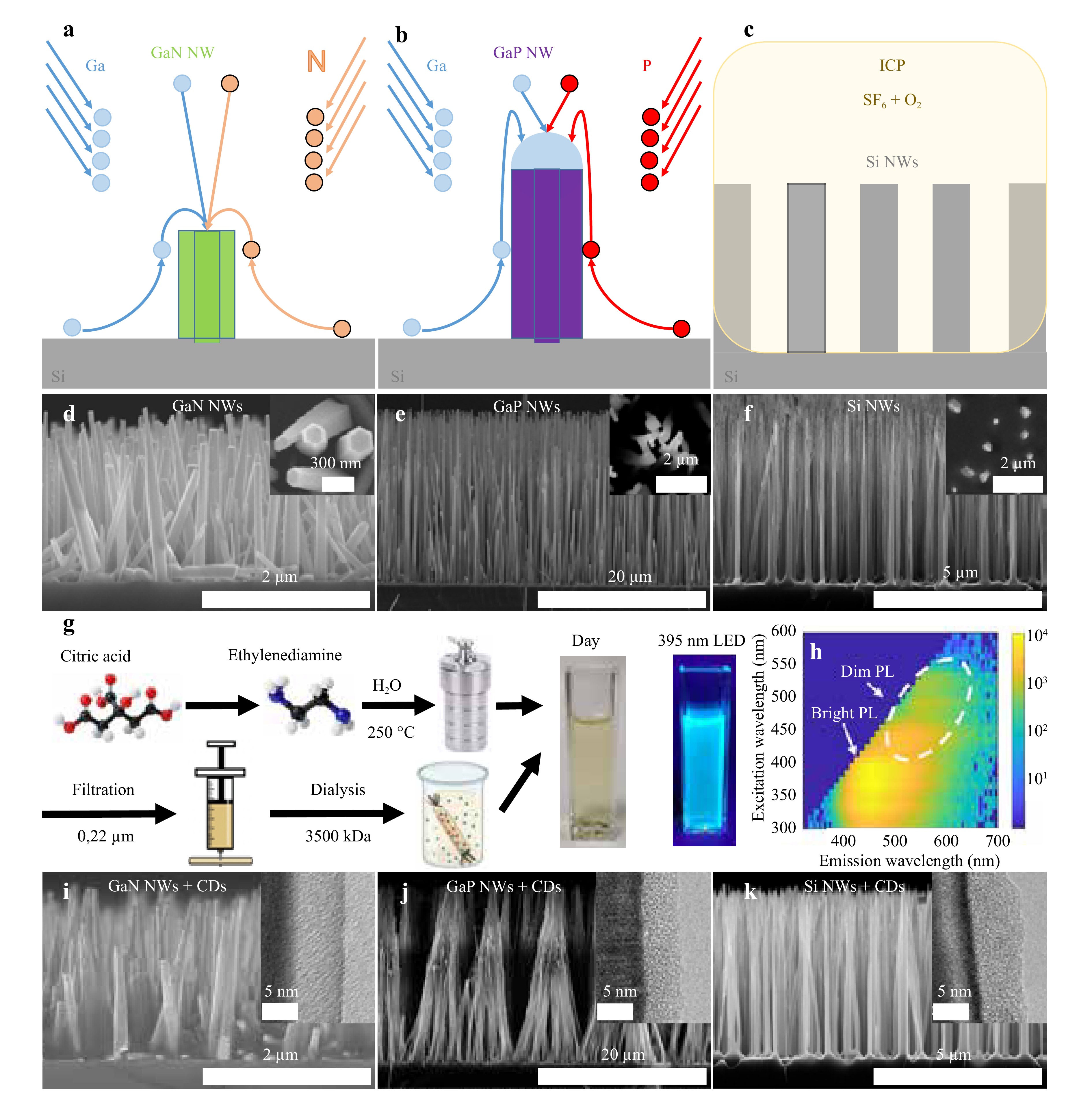
Fig. 1 Nanowires under study: a Schematic of GaN NWs synthesis by MBE via the self-induced growth mechanism. b Schematic of GaP NWs synthesis by MBE via the self-catalysed vapor-liquid-solid growth mechanism. c Schematic of Si NWs synthesis by plasma-chemical etching of a monocrystalline Si wafer. In-plane SEM images of as-grown d GaN, e GaP and f Si NWs arrays with plane view images on insets. g Step-by-step CDs’ synthesis process and photos of the cuvette with CDs aqueous solution under daylight and UV LED flashlight (395 nm, 3 W). h PL map of the CDs aqueous solution as a function of excitation wavelength (log scale). In-plane SEM images of i GaN, j GaP and k Si NWs arrays decorated with CDs, insets demonstrate corresponding TEM images of the near-surface region of the structures.
The GaN NWs utilised here, characterised by scanning electron microscopy (SEM), exhibited a high degree of morphological uniformity, with a length of approximately 2 μm and a well-defined hexagonal cross-section of ~300 nm (Fig. 1d). This structural regularity is paramount for achieving a consistent and reproducible photonic performance across the hybrid platform.
In parallel, we investigated gallium phosphide (GaP) NWs were investigated as complementary platforms for CDs integration. These NWs were synthesised directly on a (111)-oriented Si wafer via a self-catalysed vapour-liquid-solid (VLS) growth mechanism using molecular beam epitaxy (MBE)34 (Fig. 1b). GaP NWs are well suited for photonic applications because their indirect wide bandgap (~2.26 eV) confers low optical absorption across the visible and near-infrared spectral ranges. This inherent transparency makes GaP NW an exceptional optical waveguide, as confirmed by our previous work demonstrating resonant optical phenomena and highly directional guidance of light within individual NWs57,60. The waveguiding effect is a critical asset for hybrid CD-NW systems. This can lead to a significant enhancement of the local optical pumping field for CDs deposited on the NW surface. This enhancement arose from the localisation of the electromagnetic field in the near-surface region of the NW and the precise location of the CDs, thereby potentially increasing their absorption and emission efficiencies.
In addition to passive waveguiding, GaP offers a versatile approach for advanced photonic engineering. Our group has previously shown that complex heterostructured GaP(As)-based NWs can be synthesised by introducing direct-bandgap alloys that emit light in the visible range61. Furthermore, GaP NWs have proven to be excellent hosts for hybrid integration with other promising luminescent materials, such as transition metal dichalcogenides (TMDs), which serve as efficient nanoscale waveguides for emission55. This success positions GaP NWs as a robust and flexible platform for coupling with CDs. Additional favourable properties, such as a high refractive index (~3.2 at 600 nm) for strong light confinement and excellent chemical stability, further confirmed their suitability. GaP NWs used in this work, shown in Fig. 1e, are characterised by their high aspect ratio, with a length of approximately 25 μm and a uniform hexagonal cross-section with a diameter of about 300 nm. This considerable length is advantageous for studying extended waveguiding and the interaction between the propagating modes and integrated CD emitters.
Finally, we consider Si NWs, a platform whose significance is rooted in their foundational roles in modern technology. The synthesis of Si NWs is inherently compatible with the vast infrastructure of complementary metal-oxide-semiconductor (CMOS) processes, offering a direct and scalable pathway for integrating active photonic components with electronic circuitry on a single chip. This unparalleled fabrication advantage is critical for the development of commercially viable photonic platforms.
Although bulk Si is an indirect bandgap semiconductor and a poor emitter of light, its properties in NW geometry are transformative for photonics. The high refractive index (~3.5 at 600 nm) of Si provides strong optical confinement, enabling efficient waveguiding and the formation of high-quality optical resonances. Furthermore, the nanoscale morphology can lead to the relaxation of the selection rules and enhanced light-matter interactions, making Si NWs excellent passive photonic building blocks. Recent advancements have firmly established Si NWs as a leading platform for integrated nanophotonics, demonstrating functionalities such as low-loss waveguiding in the IR, optical filtering, and sensing54,62,63. Their primary utility lies in their ability to manipulate and guide light at the subwavelength scale, whereas absorption in the visible and near-infrared ranges is expected to suppress emission of the CDs.
The arrows in the schematics denote the molecular fluxes of the growth species during the MBE growth process, as well as the subsequent adatom surface diffusion along the NW sidewalls toward the growth interface.
The “cap” shown on top of the GaP NWs in Fig. 1b represents the liquid gallium (Ga) catalyst droplet, which drives the classical VLS growth mechanism. In contrast, the GaN NWs shown in Fig. 1a are grown via a self-induced (catalyst-free) mechanism, which is why they do not possess a metallic droplet at their tips.
Colours are used to distinguish between different materials and structural regions. For instance, specific colours distinguish the Si substrate from the grown III-V semiconductor materials (GaN and GaP), whereas in Fig. 1c, colour contrast is used to highlight the etched Si regions formed during the top-down inductively coupled plasma (ICP) process.
This approach bypasses the inherent emission limitations of Si and paves the way toward monolithically integrated light sources and complex photonic networks. The Si NWs utilised in this study were fabricated via the plasma-chemical etching of a boron (B)-doped monocrystalline (100) Si wafer (Fig. 1c) resulting in structures with high crystalline perfection required for consistent optical performance. The NWs have a length of approximately 10 μm and a cylindrical cross-section with a characteristic size of 300−350 nm (Fig. 1f).
CDs exhibiting blue luminescence under near-UV irradiation were synthesised using a common hydrothermal method34,64 ( Fig. 1g). Information on the PL properties of the CDs in aqueous solution is presented as an excitation-emission map in Fig. 1h. The map clearly shows the most efficient emission upon 320−400 nm excitation. The CDs exhibited bright blue emission with a peak near 450 nm under this excitation. The emission intensity decayed by an order of magnitude with an increase in the excitation wavelength, providing dim emission peaks at 550 nm under 470 nm excitation and further red-shifting to 600 nm under 550 nm excitation. Thus, we conclude that the CDs synthesised in aqueous solution exhibit bright blue luminescence upon UV excitation which shifts and gets dimmed toward green under blue excitation and further shifts to orange under green excitation.
The decoration of the NWs with CDs was carried out by drop-casting the CDs aqueous solution onto the surfaces of the GaN, GaP, and Si NWs. Because the difference in the specific surface area between the samples is governed by the difference in the NWs morphology, a CDs solution with the same concentration was used for all the samples, while its volume varied sample to sample, being proportional to the surface area of the NWs per unit area of the substrate (more details in Methods). This approach is expected to provide a uniform deposition of the CDs layer on the surfaces of NWs with different geometries. The results of this deposition are presented in Fig. 1i-k for GaN, GaP, and Si NWs. In the images obtained by transmission electron microscopy (TEM, Jeol JEM-2100, JEOL Ltd., Japan) from the near-surface region of the NWs decorated with dots, a layer of amorphous carbon coating with a thickness of approximately 5 nm was clearly visible and identical for all the samples. This layer cannot be associated with the NW material and is attributed to a layer of CDs with a thickness of 1−2 dots ( Figs. S4, S5 in Supplementary Information)34,65. The consistent CDs layer thickness observed across different NW platforms validates the applicability of the proposed volume-correcting approach. However, the deposition process also induced a morphological change in the NW arrays, leading to bundling of the NWs at their tops. This effect was most pronounced for the longest GaP NWs (Fig. 1j), likely due to capillary forces during solvent evaporation and their high mechanical flexibility34.
-
Nanostructured surfaces, including metasurfaces, are complex in terms of their optical performances. For samples with semiconductor NWs, the optical phenomena can be additionally affected by their quasi-waveguiding behaviour rather than by simple light scattering. Moreover, the NWs were non-uniform in length. To consider the influence of the NW material and dimensions on the emission spectrum of CDs placed over the NWs surface, we performed finite-difference time-domain (FDTD) modelling (see details in the Methods section). The resulting spectra, shown in Fig. 2b, e, h, demonstrate the signal scattered in the vertical upward direction by GaN, GaP, and Si NWs of different lengths. Although the simulated dipole sources initially emitted light with a uniform unity intensity across the entire wavelength range (380−800 nm), the recorded signal was generally 10 times lower and had pronounced spectral features. For example, NWs made of all three materials demonstrate broad spectral peaks in the 400−600 nm range for the smallest length NWs 0.14−1 µm. This can be explained by the fact that short NWs (with dimensions less than or approximately equal to the incident wavelengths) act as compact Mie scatterers, with a plethora of multipoles excited simultaneously.
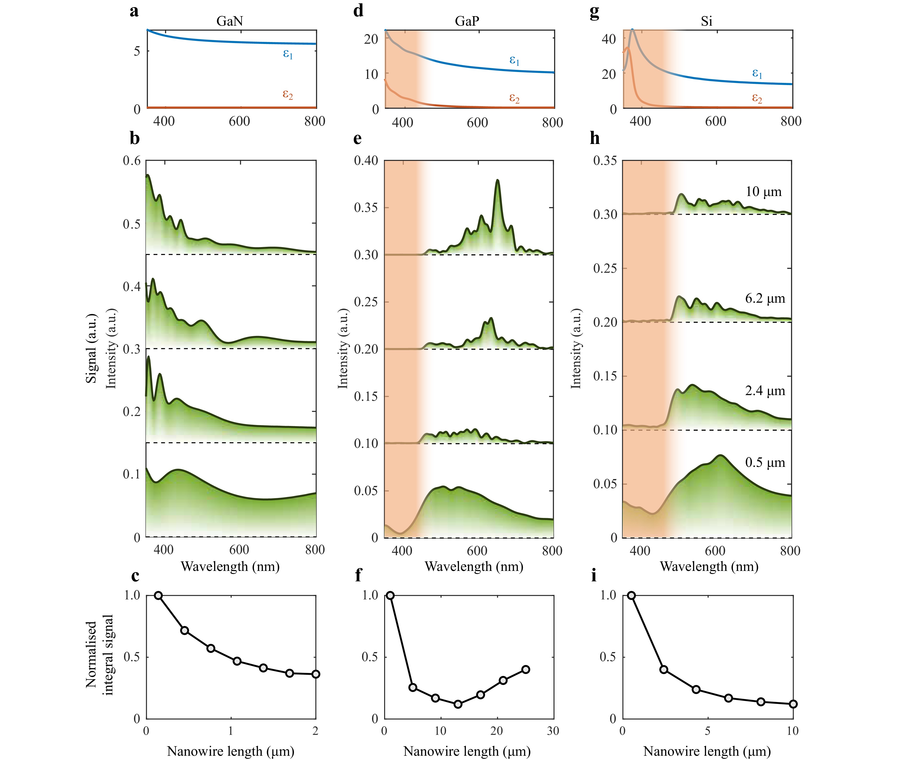
Fig. 2 PL simulation of CDs distributed along the NWs. Dielectric partitivities of a, GaN d GaP and g Si. Simulated spectra of light, emitted by point dipoles placed along the NWs and scattered by the NWs in the up direction: b GaN, e GaP and h Si. These spectra are averaged over the dipole position along the NW and dipole orientations, see Methods section for details. Integral scattered signal over the whole visible spectrum for a series of NW lengths, normalised on unity c GaN, f GaP and i Si.
The total response of the series of multipoles resulted in broad spectral features66. The spectral response changed dramatically as the NW length increased. For all three materials, the appearance of higher-frequency oscillations and redistribution of the maximum signal between several peaks were observed. We attribute this to the collective effect of the Fabry-Pérot (due to light reflections between the NW faces), Mie, and waveguide modes. The latter modes appear in the NW as the core and air as the cladding. A further increase in the NW length, up to dozens of microns, should strengthen the contribution of the waveguide modes to the total emission. This was observed for long GaP NWs. It can be seen that the integral signal over the entire visible spectrum for GaP NWs (Fig. 2c) initially decreases as the NW length increases, similar to NWs made of other materials, such as GaN and Si (Fig. 2f, i). This can be explained by the increase in the total scattering efficiency of the semidielectric NWs with increasing volume. However, starting from ~13 µm length, the signal starts to grow again. This is an effect of the waveguide modes: the light emitted by the dipoles in the vicinity of the NW surface couples to the propagating modes and is efficiently transferred to the upper face of the NWs. This mechanism should be sensitive to material loss. For the two materials under study, the optical absorption of GaP and Si is significant in the short-wavelength region, which is denoted by the red gradient strips in Fig. 2d, g. One can see that in this highly absorptive region, the scattered signal was sufficiently suppressed, as shown in Fig. 2e, h.
An analysis of the data in Fig. 2 suggests that the intrinsic optical properties of the NW substrates significantly affect the properties of the fluorescent coatings. The use of GaN favours quantum dot PL in the blue-green region of the spectrum, whereas Si and GaP NWs retain only the long-wavelength tail of the overall PL signal owing to the intrinsic optical absorption of the material.
-
To visualise luminescence, the fabricated samples were analysed using confocal fluorescence microscopy. Fig. 3a-c depicts 3D fluorescence images of the samples demonstrating luminescence over the entire surface of all the NWs. For the experiment, a 488 nm wavelength laser and a 600–660 nm bandpass filter were used to detect the response. The image acquisition conditions were identical for all three samples. It should be noted that luminescence was not observed in the bare NWs in the absence of CDs on the surface when using a 488 nm wavelength laser was used. The corresponding photon energy is insufficient to cause PL in GaN NWs, whereas GaP and Si NWs do not exhibit PL owing to their indirect bandgap structures.
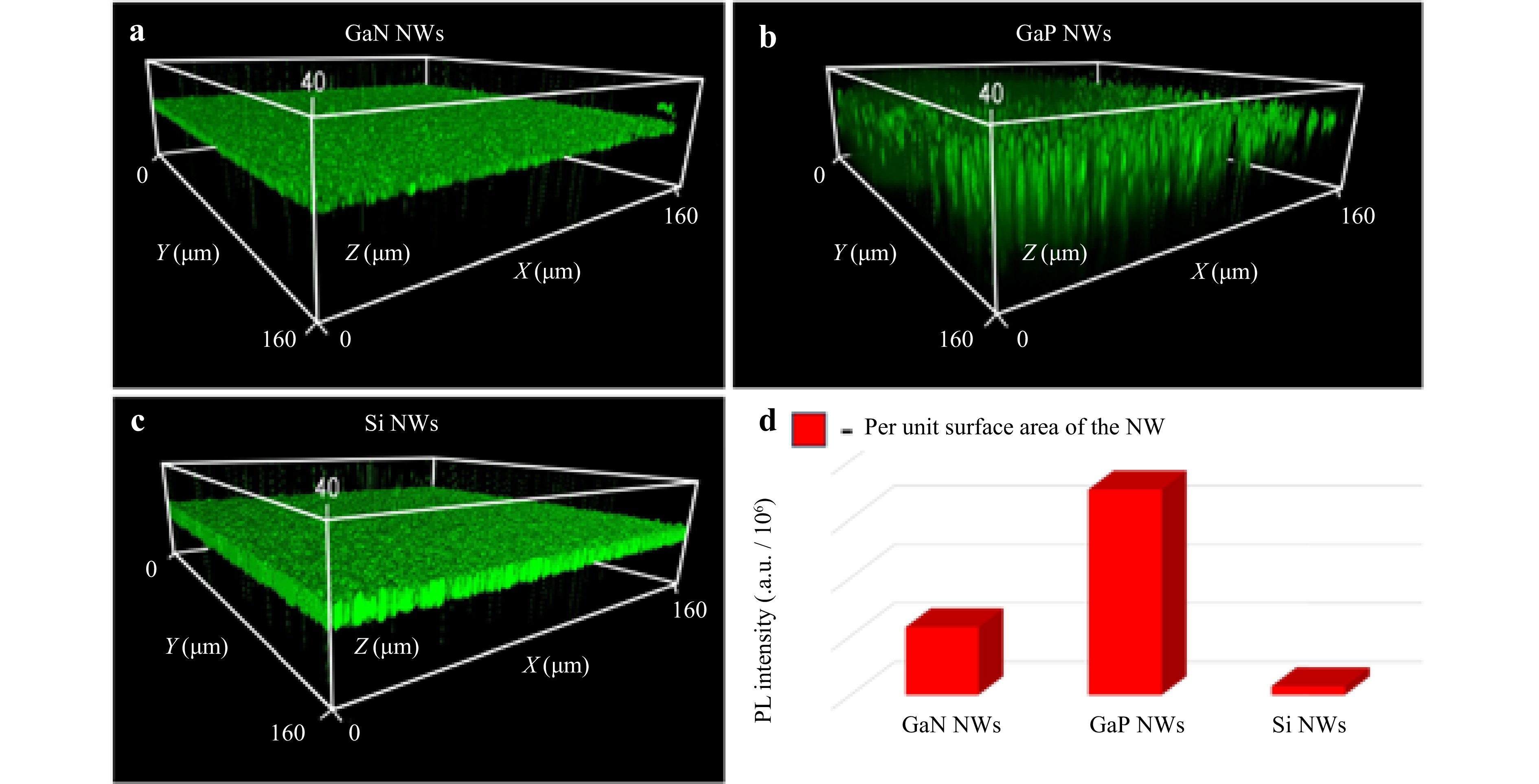
Fig. 3 NW/CDs structures confocal fluorescence microscopy. Images of the decorated a GaN, b GaP, and c Si NWs. d Histogram of the emission intensity per unit surface area of the samples.
To analyse the emission efficiency, we calculated the emission intensity of the samples by considering the sum of the pixel luminescence intensities from all the image layers. Considering the specific surface area of the NWs, the emission intensity per unit surface area of a single NW was determined. The results were 2.3 × 10⁶, 7.0 × 10⁶ and 0.3 × 10⁶ arbitrary units for GaN, GaP, and Si NWs, respectively (Fig. 3d).
Thus, the data in Fig. 1i-k and Fig. 3a-c collectively allow us to conclude the presence of a uniform layer of CDs on the surface of the NWs, exhibiting PL in the orange-red range. GaP exhibits the highest emission intensity per unit surface area for a single NW. This phenomenon is discussed in detail below:
-
To obtain more details on the PL of the NW/CD structures, we obtained the excitation-emission 2D maps presented in Fig. 4a-c. Fig. 4a shows a false-colour excitation-emission map for GaN NWs/CDs on a log scale to enhance the visibility of the major PL bands. The two most prominent ones are clearly visible on inset in Fig. 4a plotted in linear scale. These include deep level emission (DLE) in GaN NWs with a peak at 580 nm (denoted in Fig. 4a as “DLE”) at excitations 350−375 nm. The second is the dim CDs emission band peaked near 550 nm under 430 nm excitation (denoted in Fig. 4a as “CDs’ dim PL”). The occurrence of the DLE band and its origin were studied by investigating the bare GaN NWs excitation-emission map presented in the Supporting Information and demonstrating the presence of this particular band (see Fig. S1). This emission, which is known to arise from nitrogen vacancy centres, has been well documented in prior studies67.
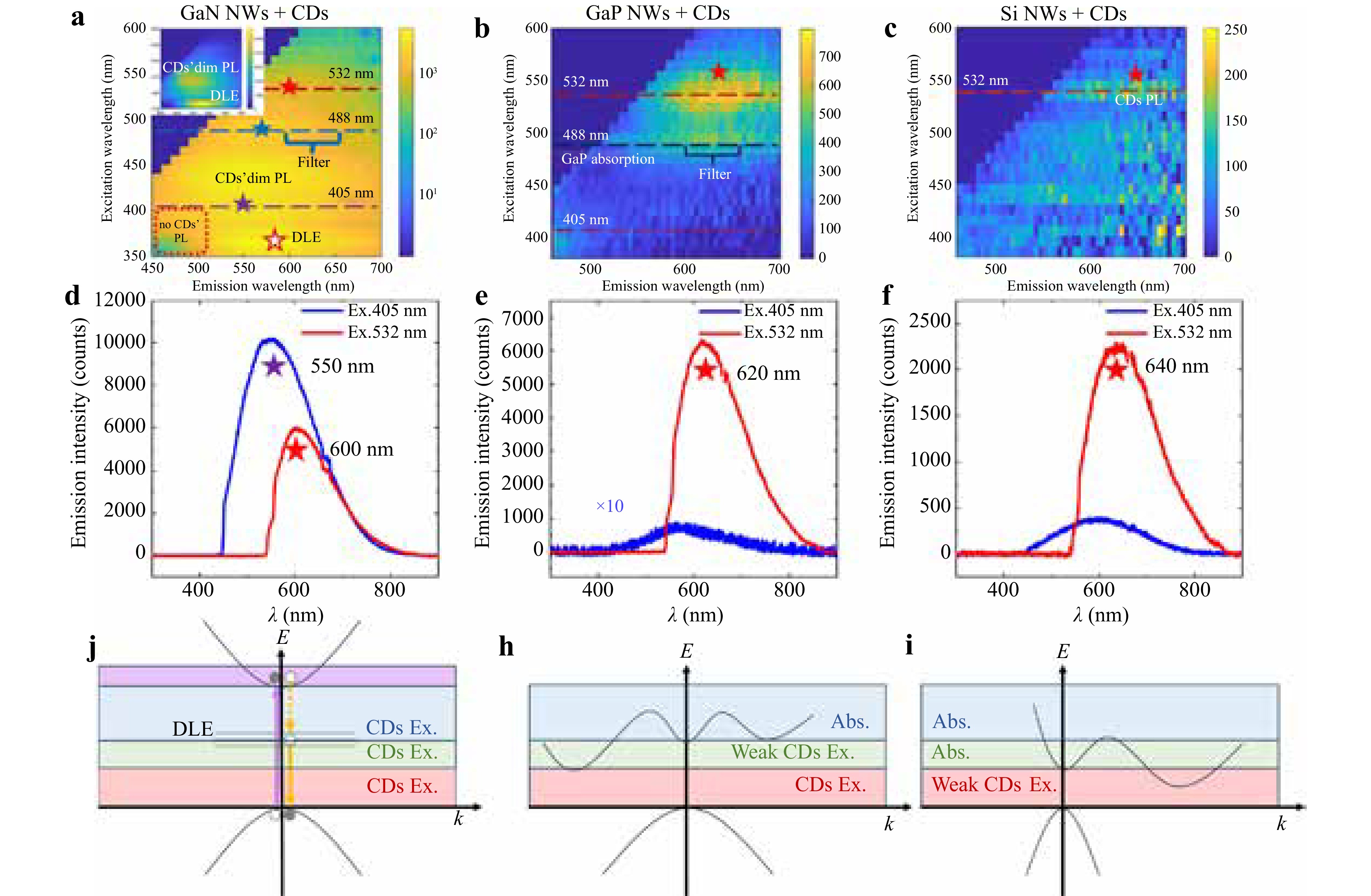
Fig. 4 NW/CDs structures PL spectroscopy. Excitation-emission maps of a GaN, b GaP, and c Si NW/CDs structures. PL spectra of d GaN, e GaP, and f Si NW/CDs structures under 405 nm and 532 nm laser excitation. Band diagrams of j GaN, h GaP, and i Si allowing for the visualisation of processes occurring during the excitation of CDs’ PL on the NW surfaces.
The dim PL observed is attributed to the CDs with a slight red shift relative to the emission of CDs in aqueous solution (Fig. 1h). This red shift is not associated with the properties of the GaN NWs but rather corresponds to the previously discussed conformational changes in the surface functional groups, leading to variations in their PL spectra.
Additionally, all the samples were investigated by PL spectroscopy under laser excitation at wavelengths of 405 and 532 nm (Fig. 4d-f). The PL spectra of the GaN NWs with CDs under both excitations depicted in Fig. 4d are in a good agreement with the map in Fig. 4a. The measurements demonstrate that the structure exhibits PL peak of CDs near 550 nm under 405 nm excitation which decays and red-shifts toward 600 nm under 532 nm excitation.
One of the most important observations with GaN NWs was the absence of blue PL CDs under UV excitation. Despite the presence of dim PL CDs under visible light excitation which is comparable in intensity to DLE, the expected bright PL peak near 450 nm was not observed. This is expected to be the result of the strong absorption of excitation in the GaN NWs which in turn results in an intense DLE. Fig. 4j depicts the GaN band diagram with highlighted ranges of excitation photon energies (the colour corresponds to the excitation), allowing interpretation of the spectroscopy data. Upon UV excitation near the absorption edge, we observed the recombination of deep-level defects in GaN. All absorption occurred in GaN; therefore, no PL corresponding to the CDs was observed. A reduction in the excitation energy below the GaN bandgap leads to excitation of the PL of the CDs, which red-shifts with an increase in the excitation wavelength.
Next, we discuss the PL of GaP NWs decorated with CDs. Fig. 4b depicts a linear-scale PL map of the sample exhibiting two major PL bands, both peaking near 620 nm: a more intense band under 532 nm and a dim band upon 488 nm excitation. These emissions correspond to the PL red shift compared with the GaN NWs. Surprisingly, no PL was observed upon excitation at wavelengths below 480 nm. This result is in perfect agreement with the PL spectra measured under 405 nm and 532 nm laser excitations, as plotted in Fig. 4e. Compared with GaN NWs, GaP NWs exhibit neither bright blue PL upon UV excitation nor dim PL below 500 nm. The latter value corresponded to the absorption edge of GaP. Thus, we confirmed that PL was not excited in the CDs below the absorption edge of the host material. The schematic of the GaP band structure in Fig. 4h shows that absorption in GaP restricts the PL excitation of CDs to the green-orange-red visible range.
Despite the calculated emission intensity per unit surface area from confocal microscopy data suggesting a threefold higher PL efficiency for CDs on GaP NWs, the excitation-emission maps in Fig. 4a, b indicate an overall higher PL intensity for the GaN-based hybrid platform. This apparent contradiction can be reconciled by considering the specific spectral conditions of different measurements. Confocal intensity values were acquired under 488 nm excitation and detected within a 600−660 nm filter window. The corresponding cross-sections on the maps in Fig. 4a, b reveal that the majority of the emission of CDs on GaN NWs lies below 600 nm, meaning that they were largely filtered out during the confocal measurement. In contrast, the most intense PL from CDs on GaP NWs was spectrally positioned within the 600−660 nm detection range, leading to preferential measurement. Furthermore, potential variations in the excitation efficiency due to sample positioning and size in broadband PL measurements introduce additional uncertainty.
Finally, we studied the Si NWs decorated with CDs. Fig. 4c depicts the PL map of the sample, showing noisy low-intensity values with a very dim band that peaked near 640 nm under 532 nm excitation. This was confirmed by PL spectroscopy under 532 nm excitation (see Fig. 4f) and corresponds to the PL of the CDs. Despite the noisy map in Fig. 4c without intense emission bands, excitation with a 405 nm laser deep inside the Si absorption band led to the measurable PL of the CDs, as shown in Fig. 4f. Again, we associated the low PL intensity throughout the entire measurement range with the absorption in the host material, Si. A schematic of the Si band structure is shown in Fig. 4i.
-
In summary, this study demonstrates a versatile and manufacturable strategy for creating nanostructured fluorescent emitters by hybridising solution-processed CDs with single-crystalline semiconductor NWs. We systematically investigated how the electronic properties of the host material dictate the photophysical response of the integrated CDs. A critical general finding is that the absorption edge of NW acts as a definitive spectral filter; efficient excitation of PL of CDs occurs only for photon energies below this edge, whereas higher-energy photons are absorbed parasitically by the host. This principle was elucidated across three distinct platforms: GaN NWs allow the broadest excitation window in the visible range, GaP NWs provide high-efficiency PL limited to the green-red spectrum, and Si NWs highlight the tradeoff between CMOS compatibility and visible-range absorption losses.
The synthesis leveraged scalable bottom-up (GaN and GaP) and top-down (Si) NW fabrication on Si substrates, ensuring a pathway for integration. Beyond spectral filtering, the NW morphology actively enhances performance through optical confinement and waveguiding, which is particularly evident in GaP structures. This study establishes a clear framework for rationally selecting host NW based on the target emission window and application. By combining the tuneable luminescence of CDs with tailored optoelectronic properties and scalable processing of semiconductor NWs, this approach offers a powerful and flexible platform for the development of integrated nanophotonic light sources for sensing, on-chip communication, and quantum technologies.
-
To understand how the NW-based morphology affects the emission signal from the deposited quantum dots, FDTD-based numerical simulations were performed. The unit cell contains a single vertically aligned NW. Although the experimental data show considerable deviations in the NW orientations from the vertical alignment, the model considers only vertically positioned NWs, as this is a critical geometric feature. The NW base diameter was set according to the SEM images shown in Fig. 1. The signal Id(λ,h,H,θ,φ) is emitted by a dipole at a certain wavelength λ, at position h along the NW (the dipole’s distance from the surface), and dipole orientation (θ,φ) along the x, y, or z axes. The carbon layer on the surface of the NWs is very thin (5 nm) and provides optical contrast between the employed semiconductor materials and carbon structures, and therefore does not introduce any noticeable perturbations in light propagation considering the large dimensions of the NWs and visible wavelengths considered. Moreover, CDs with estimated sizes 2.5 nm–5 nm physically act uniquely as light emitters68 (single dipole sources) without any optical resonant properties69,70 . GaP and GaN NWs were considered hexagonal and Si NWs cylindrical according to the morphology of the samples obtained via SEM (see Fig. 1). For every dipole arrangement, the intensity Iscat(λ,h,H,θ,φ) of the optical signal propagated through the NW and scattered upwards is recorded by a horizontally oriented field monitor placed 100 nm above the NW. To obtain the final structure-modified optical signal Ifinal, propagated through the NWs and emitted from dipoles in different arrangements, we performed the following averaging procedure:
$$ {I}_{final}\left(\lambda ,{N}_{H}\right)=\frac{1}{3{N}_{h}}\sum\limits_{\theta ,\varphi }\sum\limits_{h}\sum\limits_{H}\frac{{I}_{scat}\left(\lambda ,\mathrm{h},\mathrm{H},\theta ,\varphi \right)}{{I}_{d}\left(\lambda ,\mathrm{h},\mathrm{H},\theta ,\varphi \right)} $$ (1) where the averaging was performed over three mutually perpendicular dipole orientations and $ {N}_{h} $ dipole positions along the NW ($ {N}_{h}=5 $). Several NW lengths (NH = 6–7) were considered for each material, up to the longest experimentally observed lengths.
-
The growth experiments were performed on single-side-polished n-type Si substrates using a Riber Compact 12 MBE system. The substrate surface orientation was (111) with a 4° miscut toward the [110] direction. First, the substrate was loaded into an MBE chamber and thermally annealed at 950 °C (according to thermocouple measurements) for 20 min. Annealing of the Si substrate prior to growth was performed directly in the MBE growth chamber. The residual pressure in the chamber was ~5 × 10⁻¹¹ Torr before annealing and ~3 × 10⁻⁹ Torr and after annealing. The substrate temperature was then decreased to 600 °C, and the nitrogen plasma was ignited to form a SixNy thin layer. A SixNy layer was introduced to increase the diffusion length of the Ga adatoms and suppress parasitic GaN nucleation on the SixNy surface. In combination with preformed GaN nuclei, this approach enables relatively low-density nanowire growth; GaN growth is suppressed on the SixNy surface between the nuclei, while the nuclei act as preferential sites for subsequent GaN nanowire formation71. The plasma source was operated at a power of 450 W and a nitrogen flow rate of 0.4 sccm for 30 min. The working pressure during the growth was maintained at 7.4 × 10⁻⁶ Torr. Next, Ga was deposited onto the formed SixNy layer for 15 s in the absence of nitrogen plasma to form Ga droplets. Subsequently, the nitrogen plasma was ignited again under the same source parameters, and the surface with the Ga droplets was nitrided for 45 min. This procedure was used to form GaN nuclei that served as seeds for further GaN NW growth. Subsequently, the substrate temperature was increased to 820 °C, the Ga shutter was opened, and the growth of the GaN NWs continued for 16 h 25 min. The beam-equivalent pressure of Ga was maintained at 1.5 × 10⁻⁷ Torr throughout all stages of the growth process. This approach allows the fabrication of relatively low-density GaN NWs compared with conventional self-induced GaN NWs on Si(111) substrates.
-
The NW arrays were grown using a Veeco GEN-III solid-source MBE system equipped with a Ga effusion cell and a valved phosphorus-cracking cell. GaP NWs were formed via a self-catalytic VLS growth mechanism72 on Shiraki-cleaned73 SiOx/Si(111) wafers with a silicon oxide layer prepared via wet chemical oxidation in an aqueous solution of ammonia and hydrogen peroxide (NH4OH:H2O2:H2O with a volume ratio of 1:1:3).74 Pre-growth annealing at 780 °C for 30 min facilitated the generation of defects in the oxide layer, promoting the self-assembly of GaP NWs initiated by the simultaneous opening of the Ga and P2 fluxes. A two-stage growth procedure was implemented to independently control the length and diameter of the NWs. Details of the two-step approach are presented in a previous report75. To achieve a high yield of vertical GaP NWs, the first growth step was carried out at a high P2/Ga flux ratio of 30 and a substrate temperature of 630 °C for 33 min. In the second step, the growth was continued for 3 h at a lower V/III ratio and reduced growth temperature to obtain the desired length and diameter of the NWs. The transition to the second growth stage involved a smooth 3-fold increase in Ga flux from 3 nm/min (beam equivalent pressure of a Ga flux beam of 8 × 10⁻⁸ Torr) up to 9 nm/min (beam equivalent pressure of a Ga flux beam of 2.4 × 10⁻⁷ Torr) and a decrease in growth temperature from 630 °C to 615 °C over a period of 900 s. The growth step transition was carried out without interrupting the growth process, while maintaining a constant phosphorus flux.
-
An unpolished p-type Si (100) wafer with a resistivity of 12 Ω·cm was used. The native oxide layer was not removed prior to the etching. Cryogenic etching was performed using an Oxford Plasmalab System 100 ICP380 at a temperature of −150 °C. The SF6 and O2 gas flow rates were maintained at 50 and 11 sccm, respectively. The pressure was maintained at 5 mTorr and the ICP power was fixed at 1,000 W. An RF power (13.56 MHz) of 30 W was applied, resulting in a DC bias of 190 V. The etching time was set to 440 s. This process resulted in a uniform array of Si wires with a height of 10 µm and diameters of 300–350 nm. These wires were formed without using a mask or lithography, solely through self-organisation during the cryogenic anisotropic etching process. The residual pressure in the chamber was 10−7 Torr.
-
CDs were synthesised using a common hydrothermal method64 (Fig. 1g). The following precursors were added to the autoclave with a Teflon beaker: 1.05 g of citric acid (Sigma-Aldrich), 340 μL of ethylenediamine (Sigma-Aldrich), and 10 mL of distilled water. The solution was stirred until citric acid was completely dissolved. Then, the autoclave was placed in an oven for 5 h at 200 °C. After cooling, the reaction products were filtered through a syringe filter with a pore diameter of 0.22 μm to remove larger particles. The filtered solution was dialysed (MWCO 3.5 kDa) for 24 h to remove the low-molecular-weight compounds and unreacted residues. The photoluminescence properties of the CDs in aqueous solution were measured using a BioTek Synergy H4 Hybrid Multi-Mode Microplate Reader and are presented as an excitation-emission map in Fig. 1h.
-
The NWs were decorated with CDs by drop-casting an aqueous solution of CDs onto the surfaces of the GaN, Si, and GaP NWs. The volume of the aqueous solution was proportional to the specific surface area of the NWs per unit area of the Si substrate. The surface area of a single NW is calculated based on its geometric parameters. The lengths were 2 μm for GaN NWs, 8 μm for Si NWs, and 25 μm for GaP NWs. The characteristic diameters of the GaN, Si, and GaP were 300, 350, and 300 nm, respectively. Additionally, top-view SEM images were used to estimate the density of the NWs per unit area of the growth substrate. The estimation was performed using open-source software ImageJ (Wayne Rasband, USA). This yielded NW-to-substrate area ratios of 90 for GaN NWs, 5.5 for Si NWs, and 20 for GaN, Si, and GaP NWs, respectively. Consequently, a droplet of a specific volume was applied to each NW array. The samples were then exposed to the solution for 5 h until the CDs completely sedimented. This procedure ensured identical deposition conditions for all the NW surfaces. After 5 h, the remaining aqueous solvent was removed from the substrates using a nitrogen flow.
Although conventional approaches for forming conformal coatings on nanostructured surfaces often favour alternative methods76, we chose drop-casting for CD deposition from an aqueous solution. This approach effectively utilises capillary forces and ensures complete coating of the complex NW morphology. The liquid phase acted as a vehicle, delivering the fluorescent agent deep into the gaps between the NWs. This process resulted in a uniform luminescent coating throughout the entire height of the NW array, as clearly demonstrated by the 3D confocal photoluminescence maps (Fig. 3).
The hybrid structures fabricated using CDs from different synthesis batches exhibited the same optical behaviours and overall properties, indicating that the results reported in this study are reproducible and not dependent on a specific batch of CDs.
-
Confocal microscopy was used to analyse the samples. This technique collects luminescence from a specific optical section approximately 300 nm thick. To visualise the 3D structure, volumetric images were constructed by sequentially capturing images at 300 nm intervals (a Z-stack) and digitally stitching them together. A 488 nm laser was used for excitation, and the emitted signal was collected using a 600–660 nm bandpass filter. Images were acquired and processed using AxioVision software (Carl Zeiss Microscopy, Germany). All imaging conditions were identical for all three samples. To obtain the integral emission of the samples (Fig. 3d), the pixel luminescence intensities from all layers were summed using the Gwyddion software (GNU General Public Licence, Czech Republic, open-source software package). We also obtained the length and diameter distributions of the NWs by SEM image analysis. From these distributions, we extracted the mean geometric parameters to calculate the average surface area of the NWs per unit substrate area. The measured intensity was normalised to the calculated average area.
-
PL measurements were performed using a home-built optical setup based on ThorLab components. The setup was equipped with two continuous-wave diode laser sources (405 and 532 nm), a 10× objective (Mitutoyo M Plan Apo, NA = 0.28), and a fibre-coupled spectrometer (Optosky ATP5020P). The excitation power was set at 1 mW.
-
A BioTek Synergy H4 Hybrid Multi-Mode Microplate Reader was used to measure the photoluminescent properties of CDs in aqueous solution and on the surfaces of all three types of NWs. Although this method was originally developed for liquid-dye analysis, it can be adapted for use with solid samples by adjusting the height of the PL signal collected above the surface.
-
V.M.K. acknowledges support from the Russian Science Foundation (grant No. 25-72-00140) for the synthesis of GaP NWs and study of their morphology and optical properties, and for the numerical modelling. A.V.S. acknowledges support of the TEM studies by the Russian Science Foundation (Grant No. 25-12-00154). S.V.B. acknowledges support of spectral fluorimetry from the Ministry of Science and Higher Education (Agreement No. 075-03-2025-662, project FSMG-2025-0003). M.A.A. thanks the Ministry of Science and Higher Education of the Russian Federation (project FSMG-2025-0005) for support of optical spectroscopy. A.D.B. acknowledges Russian Science Foundation (Grant 24-12-00225) for support of samples preparation. A.S.G. acknowledges the support from the Ministry of Science and Higher Education of the Russian Federation (research project 0791-2026-0035) for the synthesis of Si NWs (Si fibres). E.P.K., K.P.K. and I.S.M. thank the Ministry of Science and Higher Education of the Russian Federation (Grant FSRM-2026-0004) for supporting the processing, SEM studies and manipulation of the NWs and CDs. V.O.G., T.Sh., and G.E.C. acknowledge Saint-Petersburg State University for the GaN nanowire growth (research project 122040800254-4).
Host-engineered carbon dot luminescence: integration with nanowires for photonics
- Light: Advanced Manufacturing , Article number: 75 (2026)
- Received: 30 January 2026
- Revised: 23 April 2026
- Accepted: 24 April 2026 Published online: 22 July 2026
doi: https://doi.org/10.37188/lam.2026.075
Abstract: The integration of luminescent nanomaterials into scalable semiconductor platforms is vital for on-chip photonics. This study demonstrates an approach to fabricate fluorescent nanostructures by hybridising carbon dots (CDs) with semiconductor nanowires (NWs) grown on Si. We systematically investigated the photoluminescence of CDs on GaN, GaP, and Si NW hosts and demonstrated the key role of the absorption edge of the host as a practical spectral filter. Our results show that efficient CD excitation is governed by the transparency window of the NW, thereby allowing the precise tailoring of the emission spectrum through rational host selection. This effect has been consistently demonstrated in different materials. By coupling the tuneable chemistry of CDs with the tailored optoelectronics of semiconductor NWs, this study establishes a scalable host-guest architecture for engineering nanoscale light sources to promote applications in integrated photonic circuits and sensing.
Research Summary
Nanophotonics: Semiconductor nanowires act as spectral filters for carbon dots
Integrating luminescent carbon dots with semiconductor nanowires makes hybrid nanoscale light sources that can be precisely tuned for integrated photonic circuits and sensing applications. Valeriy M. Kondratev, Alexey D. Bolshakov, and colleagues systematically integrated carbon dots onto silicon, gallium nitride, and gallium phosphide nanowires. They discovered that the absorption edge of the host nanowire functions as a practical spectral filter. Efficient excitation of the carbon dots only occurs within the nanowire's transparency window, meaning higher-energy photons are absorbed by the host instead. This hybrid architecture provides a scalable method to engineer emission spectra, offering a flexible platform for developing advanced light sources in on-chip communication and quantum technologies.
Rights and permissions
Open Access This article is licensed under a Creative Commons Attribution 4.0 International License, which permits use, sharing, adaptation, distribution and reproduction in any medium or format, as long as you give appropriate credit to the original author(s) and the source, provide a link to the Creative Commons license, and indicate if changes were made. The images or other third party material in this article are included in the article′s Creative Commons license, unless indicated otherwise in a credit line to the material. If material is not included in the article′s Creative Commons license and your intended use is not permitted by statutory regulation or exceeds the permitted use, you will need to obtain permission directly from the copyright holder. To view a copy of this license, visit http://creativecommons.org/licenses/by/4.0/.

 DownLoad: